

GSI TECHNOLOGY GS88237AB-250, GS88237AB-225, GS88237AB-200, GS88237AB-166, GS88237AB-150 Service Manual
...
查询GS88237AB-133供应商
GS88237AB-250/225/200/166/150/133
119-Bump BGA
256K x 36
Commercial Temp
Industrial Temp
9Mb Synchronous Burst SRAMs
Features
• Single/Dual Cycle Deselect selectable
• IEEE 1149.1 JTAG-compatible Boundary Scan
• ZQ mode pin for user-selectable high
• 2.5 V or 3.3 V +10%/–10% core power supply
• 2.5 V or 3.3 V I/O supply
pin for Linear or Interleaved Burst mode
• LBO
• Internal input resistors on mode pins allow floating mode pins
• Byte Write (BW
• Internal self-timed write cycle
• Automatic power-down for portable applications
• JEDEC-standard 119-bump BGA package
) and/or Global Write (GW) operation
/low output drive
Functional Description
Applications
The GS88237AB is a 9,437,184-bit high performance
synchronous SRAM with a 2-bit burst address counter. Although
of a type originally developed for Level 2 Cache applications
supporting high performance CPUs, the device now finds
application in synchronous SRAM applications, ranging from
DSP main store to networking chip set support.
Controls
Addresses, data I/Os, chip enable (E1), address burst control
inputs (ADSP
) are synchronous and are controlled by a positive-edge-
GW
triggered clock input (CK). Output enable (G
control (ZZ) are asynchronous inputs. Burst cycles can be initiated
with either ADSP
burst addresses are generated internally and are controlled by
. The burst address counter may be configured to count in
ADV
either linear or interleave order with the Linear Burst Order (LBO
input. The Burst function need not be used. New addresses can be
loaded on every cycle with no degradation of chip performance.
, ADSC, ADV), and write control inputs (Bx, BW,
) and power down
or ADSC inputs. In Burst mode, subsequent
250 MHz–133 MHz
2.5 V or 3.3 V V
2.5 V or 3.3 V I/O
SCD and DCD Pipelined Reads
The GS88237AB is a SCD (Single Cycle Deselect) and DCD
(Dual Cycle Deselect) pipelined synchronous SRAM.
SRAMs pipeline disable commands to the same degree as read
commands. SCD SRAMs pipeline deselect commands one stage
less than read commands. SCD RAMs begin turning off their
outputs immediately after the deselect command has been
captured in the input registers. DCD RAMs hold the deselect
command for one full cycle and then begin turning off their
outputs just after the second rising edge of clock. The user may
configure this SRAM for either mode of operation using the SCD
mode input.
Byte Write and Global Write
Byte write operation is performed by using Byte Write enable
) input combined with one or more individual byte write
(BW
signals (Bx
writing all bytes at one time, regardless of the Byte Write control
inputs.
FLXDrive™
The ZQ pin allows selection between high drive strength (ZQ low)
for multi-drop bus applications and normal drive strength (ZQ
floating or high) point-to-point applications. See the Output Driver
Characteristics chart for details.
Sleep Mode
Low power (Sleep mode) is attained through the assertion (High)
of the ZZ signal, or by stopping the clock (CK). Memory data is
retained during Sleep mode.
Core and Interface Voltages
The GS88237AB operates on a 2.5 V or 3.3 V power supply. All
input are 3.3 V and 2.5 V compatible. Separate output power
)
(V
DDQ
circuits and are 3.3 V and 2.5 V compatible.
). In addition, Global Write (GW) is available for
) pins are used to decouple output noise from the internal
DD
DCD
Parameter Synopsis
-250 -225 -200 -166 -150 -133 Unit
Pipeline
3-1-1-1
3.3 V Current 330 300 270 230 215 190 mA
2.5 V Current 320 295 265 225 210 185 mA
Rev: 1.02 11/2004 1/28 © 2002, GSI Technology
Specifications cited are subject to change without notice. For latest documentation see http://www.gsitechnology.com.
t
KQ
tCycle
2.0
4.0
2.2
4.4
2.5
5.0
2.9
6.0
3.3
6.7
3.5
7.5nsns
GS88237AB-250/225/200/166/150/133
GS88237A Pad Out—119-Bump BGA—Top View (Package B)
1234567
A
B
C
D
E
F
G
H
J
K
L
V
DDQ
NC NC A ADSC AANC
NC A A V
DQC DQPC V
DQC DQC V
V
DDQ
DQC DQC BC ADV BB DQB DQB
DQC DQC V
V
DDQ
DQD DQD V
DQD DQD BD SCD BA DQA DQA
A A ADSP AAV
AANC
DQPB DQB
SS
SS
SS
SS
NC V
SS
DQB DQB
DQB V
DQB DQB
DD
DQA DQA
DQC V
V
DD
SS
SS
SS
SS
NC V
SS
DD
ZQ V
E1 V
G V
GW V
DD
CK V
V
DDQ
DDQ
DDQ
M
N
P
R
T
U
V
DDQ
DQD DQD V
DQD DQPD V
NC A LBO V
NC NC A A A NC ZZ
V
DDQ
DQD V
SS
SS
SS
BW V
A1 V
A0 V
V
DD
SS
SS
SS
DDQ
DNU
DQA V
DQA DQA
DQPA DQA
/
APE
TMS TDI TCK TDO NC V
DDQ
DDQ
Rev: 1.02 11/2004 2/28 © 2002, GSI Technology
Specifications cited are subject to change without notice. For latest documentation see http://www.gsitechnology.com.
GS88237AB-250/225/200/166/150/133
GS88237A BGA Pin Description
Symbol Type Description
A0, A1 I Address field LSBs and Address Counter Preset Inputs
An I Address Inputs
DQ
A
DQB
DQC
DQD
B
A, BB, BC, BD I Byte Write Enable for DQA, DQB, DQC, DQD I/Os; active low (x36 Version)
NC — No Connect
CK I Clock Input Signal; active high
BW
GW
E
1 I Chip Enable; active low
G
ADV
ADSP
, ADSC I Address Strobe (Processor, Cache Controller); active low
ZZ I Sleep Mode control; active high
LBO
SCD
PE
ZQ
TMS
TDI
TDO
TCK
V
DD
V
SS
V
DDQ
V
/DNU
DDQ
I/O Data Input and Output pins
I Byte Write—Writes all enabled bytes; active low
I Global Write Enable—Writes all bytes; active low
I Output Enable; active low
I Burst address counter advance enable; active low
I Linear Burst Order mode; active low
I Single Cycle Deselect/Dual Cycle Deselect Mode Control
I Parity Bit Enable; active low (High = x16/32 Mode, Low = x18/36 Mode)
I
(Low = Low Impedance [High Drive], High = High Impedance [Low Drive])
FLXDrive Output Impedance Control
I Scan Test Mode Select
I Scan Test Data In
O Scan Test Data Out
I Scan Test Clock
I Core power supply
I I/O and Core Ground
I Output driver power supply
or V
(must be tied high)
DD
or
—
V
DDQ
Do Not Use (must be left floating)
Rev: 1.02 11/2004 3/28 © 2002, GSI Technology
Specifications cited are subject to change without notice. For latest documentation see http://www.gsitechnology.com.
GS88237AB-250/225/200/166/150/133
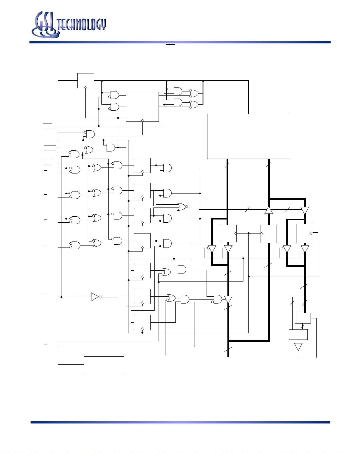
GS88237A (PE = 0) Block Diagram
A0–An
LBO
ADV
CK
ADSC
ADSP
GW
BW
BA
BB
BC
BD
Register
DQ
A0
A1
D0
D1
Counter
Load
Register
DQ
Register
DQ
Register
DQ
Register
DQ
Q0
Q1
A0
A1
A
Memory
Array
QD
36
4
DQ
Register
36
4
Register
DQ
Register
DQ
E1
1
G
ZZ
Power Down
Control
Register
DQ
Register
DQ
Register
DQ
36
36
36
DQx1–DQx9
36
36
4
Compare
Parity
Encode
Parity
NC
32
4
NC
Note: Only x36 version shown for simplicity.
Rev: 1.02 11/2004 4/28 © 2002, GSI Technology
Specifications cited are subject to change without notice. For latest documentation see http://www.gsitechnology.com.
GS88237AB-250/225/200/166/150/133
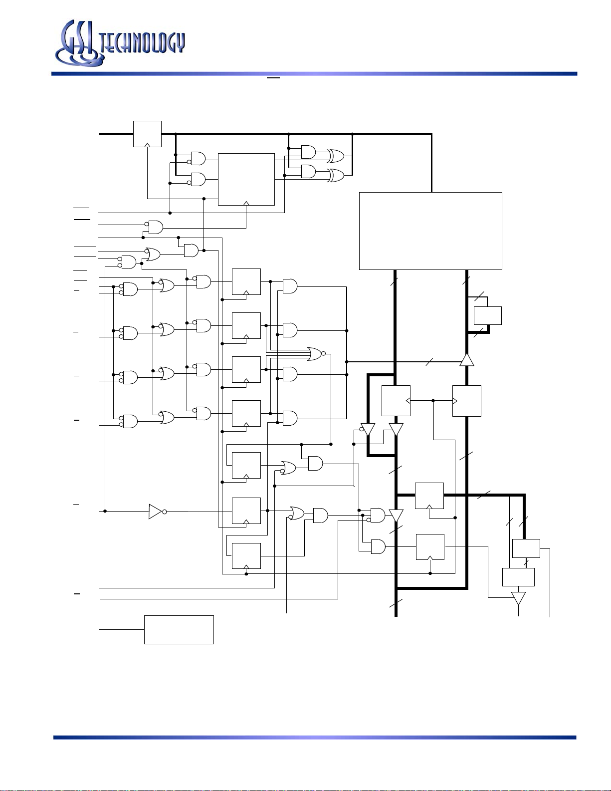
GS88237A (PE = 1) x32 Mode Block Diagram
A0–An
LBO
ADV
CK
ADSC
ADSP
GW
BW
BA
BB
BC
BD
Register
DQ
A0
A1
D0
D1
Counter
Load
Register
DQ
Register
DQ
Register
DQ
Register
DQ
Q0
Q1
A0
A1
A
Memory
Array
QD
36
4
DQ
Register
DQ
36
4
Parity
Encode
32
Register
E1
1
G
ZZ
Power Down
Control
Note: Only x36 version shown for simplicity.
Register
DQ
Register
DQ
Register
DQ
36
32
32
DQx1–DQx9
Register
DQ
Register
DQ
32
36
4
32
Parity
Encode
4
Parity
Compare
NC
NC
Rev: 1.02 11/2004 5/28 © 2002, GSI Technology
Specifications cited are subject to change without notice. For latest documentation see http://www.gsitechnology.com.
Mode Pin Functions
GS88237AB-250/225/200/166/150/133
Mode Name
Burst Order Control LBO
Power Down Control ZZ
Note:
There is a pull-down device on the ZZ pin, so this input pin can be unconnected and the chip will operate in the default states as specified in the
above tables.
Burst Counter Sequences
A[1:0] A[1:0] A[1:0] A[1:0]
1st address 00 01 10 11
2nd address 01 10 11 00
3rd address 10 11 00 01
4th address 11 00 01 10
Note:
The burst counter wraps to initial state on the 5th clock.
Pin
Name
State Function
L Linear Burst
H Interleaved Burst
L or NC Active
H
Standby, I
Note:
The burst counter wraps to initial state on the 5th clock.
DD
1st address 00 01 10 11
2nd address 01 00 11 10
3rd address 10 11 00 01
4th address 11 10 01 00
= I
SB
A[1:0] A[1:0] A[1:0] A[1:0]
BPR 1999.05.18
Rev: 1.02 11/2004 6/28 © 2002, GSI Technology
Specifications cited are subject to change without notice. For latest documentation see http://www.gsitechnology.com.
GS88237AB-250/225/200/166/150/133
Byte Write Truth Table
Function GW BW BA BB BC BD Notes
Read H H X X X X 1
Read HLHHHH1
Write byte a H L L H H H 2, 3
Write byte b H L H L H H 2, 3
Write byte c H L H H L H 2, 3, 4
Write byte d H L H H H L 2, 3, 4
Write all bytesHLLLLL2, 3, 4
Write all bytesLXXXXX
Notes:
1. All byte outputs are active in read cycles regardless of the state of Byte Write Enable inputs.
2. Byte Write Enable inputs B
3. All byte I/Os remain High-Z during all write operations regardless of the state of Byte Write Enable inputs.
4. Bytes “
C” and “D” are only available on the x36 version.
A, BB, BC, and/or BD may be used in any combination with BW to write single or multiple bytes.
Rev: 1.02 11/2004 7/28 © 2002, GSI Technology
Specifications cited are subject to change without notice. For latest documentation see http://www.gsitechnology.com.
GS88237AB-250/225/200/166/150/133
Synchronous Truth Table
State
Operation Address Used
Deselect Cycle, Power Down None X H X L X X High-Z
Read Cycle, Begin Burst External R L L X X X Q
Read Cycle, Begin Burst External R L H L X F Q
Write Cycle, Begin Burst External W L H L X T D
Read Cycle, Continue Burst Next CR X H H L F Q
Read Cycle, Continue Burst Next CR H X H L F Q
Write Cycle, Continue Burst Next CW X H H L T D
Write Cycle, Continue Burst Next CW H X H L T D
Read Cycle, Suspend Burst Current X H H H F Q
Read Cycle, Suspend Burst Current H X H H F Q
Diagram
5
Key
E1 ADSP ADSC ADV
W
3
DQ
4
Write Cycle, Suspend Burst Current X H H H T D
Write Cycle, Suspend Burst Current H X H H T D
Notes:
1. X = Don’t Care, H = High, L = Low
2. W = T (True) and F (False) is defined in the Byte Write Truth Table preceding
3. G
is an asynchronous input. G can be driven high at any time to disable active output drivers. G low can only enable active drivers (shown
as “Q” in the Truth Table above).
4. All input combinations shown above are tested and supported. Input combinations shown in gray boxes need not be used to accomplish
basic synchronous or synchronous burst operations and may be avoided for simplicity.
5. Tying ADSP
6. Tying ADSP
high and ADSC low allows simple non-burst synchronous operations. See BOLD items above.
high and ADV low while using ADSC to load new addresses allows simple burst operations. See ITALIC items above.
Rev: 1.02 11/2004 8/28 © 2002, GSI Technology
Specifications cited are subject to change without notice. For latest documentation see http://www.gsitechnology.com.
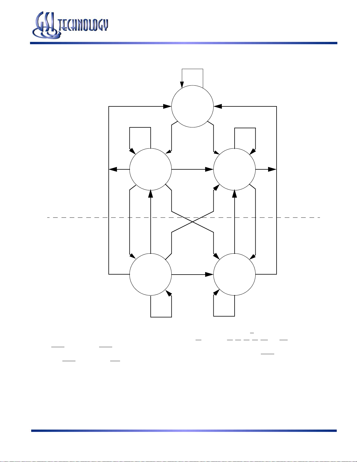
Simplified State Diagram
X
Deselect
WR
GS88237AB-250/225/200/166/150/133
Simple Synchronous OperationSimple Burst Synchronous Operation
W
X
First Write
WR
Burst Write
CW CR
R
CR
R
CR
R
First Read
Burst Read
X
CRCW
XX
Notes:
1. The diagram shows only supported (tested) synchronous state transitions. The diagram presumes G
2. The upper portion of the diagram assumes active use of only the Enable (E1
that ADSP
3. The upper and lower portions of the diagram together assume active use of only the Enable, Write, and ADSC
assumes ADSP
Rev: 1.02 11/2004 9/28 © 2002, GSI Technology
Specifications cited are subject to change without notice. For latest documentation see http://www.gsitechnology.com.
is tied high and ADSC is tied low.
is tied high and ADV is tied low.
) and Write (BA, BB, BC, BD, BW, and GW) control inputs, and
is tied low.
control inputs and
 Loading...