

GSI Technology GS8662R08-333, GS8662R09-333, GS8662R18-333, GS8662R36E-333, GS8662R08-300 Service Manual
...
Preliminary
GS8662R08/09/18/36E-333/300/250/200/167
165-Bump BGA
72Mb SigmaCIO DDR-II
Commercial Temp
Industrial Temp
Burst of 4 SRAM
Features
• Simultaneous Read and Write SigmaCIO™ Interface
• Common I/O bus
• JEDEC-standard pinout and package
• Double Data Rate interface
• Byte Write (x36 and x18) and Nybble Write (x8) function
• Burst of 4 Read and Write
• 1.8 V +100/–100 mV core power supply
• 1.5 V or 1.8 V HSTL Interface
• Pipelined read operation with self-timed Late Write
• Fully coherent read and write pipelines
• ZQ pin for programmable output drive strength
• IEEE 1149.1 JTAG-compliant Boundary Scan
• Pin-compatible with present 9Mb, 18Mb, 36Mb and future
144Mb devices
• 165-bump, 15 mm x 17 mm, 1 mm bump pitch BGA package
• RoHS-compliant 165-bump BGA package available
SigmaCIO™ Family Overview
The GS8662R08/09/18/36E are built in compliance with the
SigmaCIO DDR-II SRAM pinout standard for Common I/O
synchronous SRAMs. They are 75,497,472-bit (72Mb)
SRAMs. The GS8662R08/09/18/36E SigmaCIO SRAMs are
just one element in a family of low power, low voltage HSTL
I/O SRAMs designed to operate at the speeds needed to
implement economical high performance networking systems.
Clocking and Addressing Schemes
The GS8662R08/09/18/36E SigmaCIO DDR-II SRAMs are
synchronous devices. They employ two input register clock
inputs, K and
inputs, not differential inputs to a single differential clock input
buffer. The device also allows the user to manipulate the
output register clock inputs quasi independently with the C and
C clock inputs. C and
K. K and K are independent single-ended clock
C are also independent single-ended
333 MHz–167 MHz
1.8 V V
DD
1.8 V and 1.5 V I/O
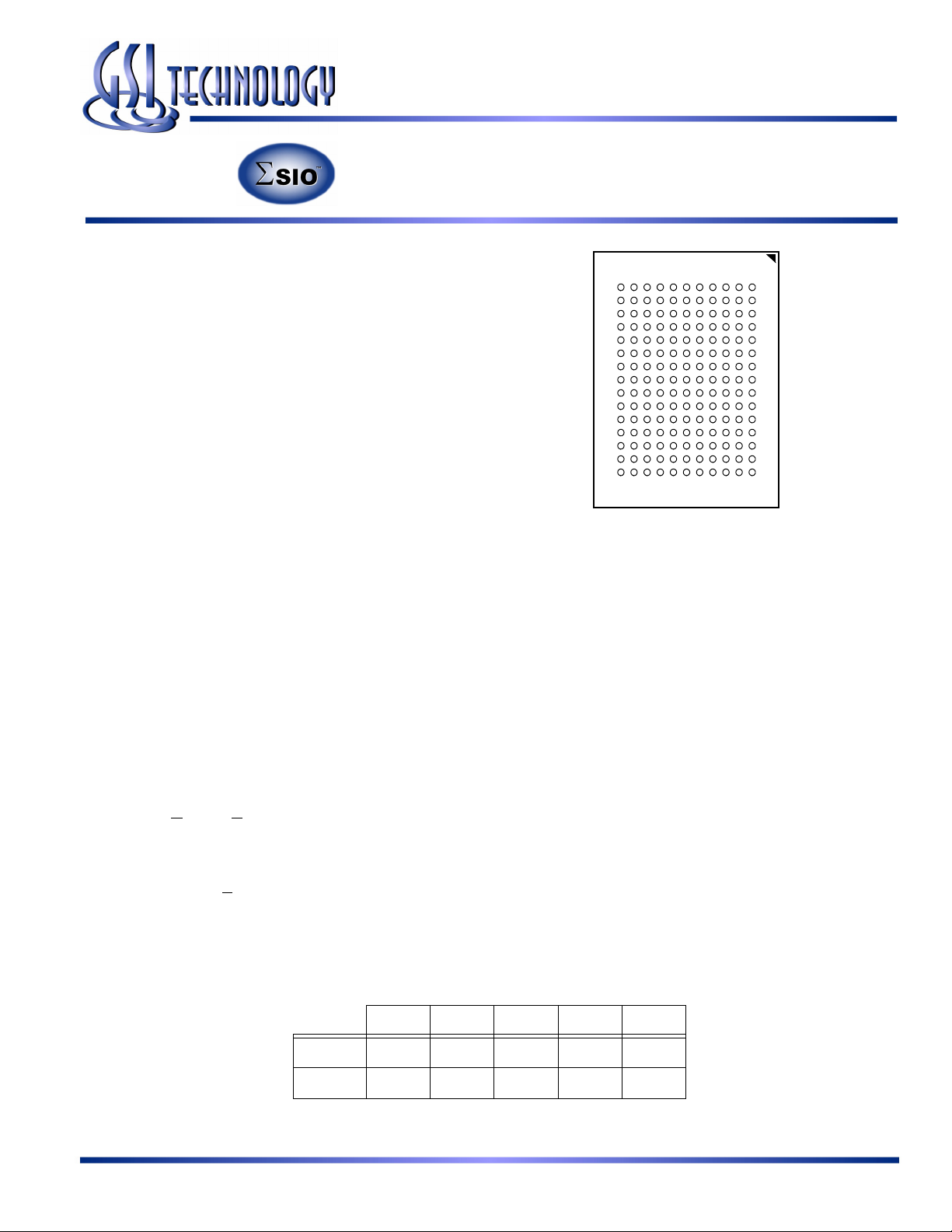
Bottom View
165-Bump, 15 mm x 17 mm BGA
1 mm Bump Pitch, 11 x 15 Bump Array
clock inputs, not differential inputs. If the C clocks are tied
high, the K clocks are routed internally to fire the output
registers instead.
Common I/O x36 and x18 SigmaCIO DDR-II B4 RAMs
always transfer data in four packets. When a new address is
loaded, A0 and A1 preset an internal 2 bit linear address
counter. The counter increments by 1 for each beat of a burst of
four data transfer. The counter always wraps to 00 after
reaching 11, no matter where it starts.
Common I/O x8 SigmaCIO DDR-II B4 RAMs always transfer
data in four packets. When a new address is loaded, the LSBs
are internally set to 0 for the first read or write transfer, and
incremented by 1 for the next 3 transfers. Because the LSBs
are tied off internally, the address field of a x8 SigmaCIO
DDR-II B4 RAM is always two address pins less than the
advertised index depth (e.g., the 4M x 18 has a 1024K
addressable index).
Parameter Synopsis
-333 -300 -250 -200 -167
tKHKH 3.0 ns 3.3 ns 4.0 ns 5.0 ns 6.0 ns
tKHQV 0.45 ns 0.45 ns 0.45 ns 0.45 ns 0.5 ns
Rev: 1.01 9/2005 1/37 © 2005, GSI Technology
Specifications cited are subject to change without notice. For latest documentation see http://www.gsitechnology.com.
Preliminary
GS8662R08/09/18/36E-333/300/250/200/167
2M x 36 SigmaCIO DDR-II SRAM—Top View
1 2 3 4 5 6 7 8 9 10 11
A CQ
MCL/SA
(144Mb)
SA R/W BW2 K BW1 LD SA SA CQ
B NC DQ27 DQ18 SA BW3 K BW0 SA NC NC DQ8
C NC NC DQ28 V
D NC DQ29 DQ19 V
E NC NC DQ20 V
F NC DQ30 DQ21 V
G NC DQ31 DQ22 V
H Doff V
REF
V
DDQ
V
J NC NC DQ32 V
K NC NC DQ23 V
L NC DQ33 DQ24 V
M NC NC DQ34 V
SS
SS
DDQ
DDQ
DDQ
DDQ
DDQ
DDQ
DDQ
SS
SA SA0 SA1 V
V
SS
V
SS
V
DD
V
DD
V
DD
V
DD
V
DD
V
SS
V
SS
V
SS
V
SS
V
SS
V
SS
V
SS
V
SS
V
SS
V
SS
V
SS
V
SS
V
SS
V
DD
V
DD
V
DD
V
DD
V
DD
V
SS
V
SS
SS
V
SS
V
DDQ
V
DDQ
V
DDQ
V
DDQ
V
DDQ
V
DDQ
V
DDQ
V
SS
NC DQ17 DQ7
NC NC DQ16
NC DQ15 DQ6
NC NC DQ5
NC NC DQ14
V
DDQ
V
REF
NC DQ13 DQ4
NC DQ12 DQ3
NC NC DQ2
NC DQ11 DQ1
ZQ
N NC DQ35 DQ25 V
SS
SA SA SA V
SS
NC NC DQ10
P NC NC DQ26 SA SA C SA SA NC DQ9 DQ0
R TDO TCK SA SA SA C SA SA SA TMS TDI
11 x 15 Bump BGA—13 x 15 mm2 Body—1 mm Bump Pitch
Notes:
1. BW0 controls writes to DQ0:DQ8; BW1 controls writes to DQ9:DQ17; BW2 controls writes to DQ18:DQ26; BW3 controls writes to
DQ27:DQ35
2. MCL = Must Connect Low
Rev: 1.01 9/2005 2/37 © 2005, GSI Technology
Specifications cited are subject to change without notice. For latest documentation see http://www.gsitechnology.com.
Preliminary
GS8662R08/09/18/36E-333/300/250/200/167
4M x 18 SigmaCIO DDR-II SRAM—Top View
1 2 3 4 5 6 7 8 9 10 11
A CQ SA SA R/W BW1 K NC LD SA SA CQ
B NC DQ9 NC SA NC K BW0 SA NC NC DQ8
C NC NC NC V
D NC NC DQ10 V
E NC NC DQ11 V
F NC DQ12 NC V
G NC NC DQ13 V
H Doff V
REF
V
DDQ
V
J NC NC NC V
K NC NC DQ14 V
L NC DQ15 NC V
M NC NC NC V
N NC NC DQ16 V
SS
SS
DDQ
DDQ
DDQ
DDQ
DDQ
DDQ
DDQ
SS
SS
SA SA0 SA1 V
V
SS
V
SS
V
DD
V
DD
V
DD
V
DD
V
DD
V
SS
V
SS
V
SS
V
SS
V
SS
V
SS
V
SS
V
SS
V
SS
V
SS
V
SS
V
SS
V
SS
V
DD
V
DD
V
DD
V
DD
V
DD
V
SS
V
SS
SA SA SA V
SS
V
SS
V
DDQ
V
DDQ
V
DDQ
V
DDQ
V
DDQ
V
DDQ
V
DDQ
V
SS
SS
NC DQ7 NC
NC NC NC
NC NC DQ6
NC NC DQ5
NC NC NC
V
DDQ
V
REF
NC DQ4 NC
NC NC DQ3
NC NC DQ2
NC DQ1 NC
NC NC NC
ZQ
P NC NC DQ17 SA SA C SA SA NC NC DQ0
R TDO TCK SA SA SA C SA SA SA TMS TDI
11 x 15 Bump BGA—13 x 15 mm2 Body—1 mm Bump Pitch
Notes:
1. BW0 controls writes to DQ0:DQ8; BW1 controls writes to DQ9:DQ17
2. MCL = Must Connect Low
Rev: 1.01 9/2005 3/37 © 2005, GSI Technology
Specifications cited are subject to change without notice. For latest documentation see http://www.gsitechnology.com.

Preliminary
GS8662R08/09/18/36E-333/300/250/200/167
8M x 9 SigmaCIO DDR-II SRAM—Top View
1 2 3 4 5 6 7 8 9 10 11
A CQ SA SA R/W NC K NC LD SA SA CQ
B NC NC NC SA NC K BW SA NC NC DQ4
C NC NC NC V
D NC NC NC V
E NC NC DQ5 V
F NC NC NC V
G NC NC DQ6 V
H Doff V
REF
V
DDQ
V
J NC NC NC V
K NC NC NC V
L NC DQ7 NC V
M NC NC NC V
N NC NC NC V
SS
SS
DDQ
DDQ
DDQ
DDQ
DDQ
DDQ
DDQ
SS
SS
SA NC SA V
V
SS
V
SS
V
DD
V
DD
V
DD
V
DD
V
DD
V
SS
V
SS
V
SS
V
SS
V
SS
V
SS
V
SS
V
SS
V
SS
V
SS
V
SS
V
SS
V
SS
V
DD
V
DD
V
DD
V
DD
V
DD
V
SS
V
SS
SA SA SA V
SS
V
SS
V
DDQ
V
DDQ
V
DDQ
V
DDQ
V
DDQ
V
DDQ
V
DDQ
V
SS
SS
NC NC NC
NC NC NC
NC NC DQ3
NC NC NC
NC NC NC
V
DDQ
V
REF
NC DQ2 NC
NC NC NC
NC NC DQ1
NC NC NC
NC NC NC
ZQ
P NC NC DQ8 SA SA C SA SA NC NC DQ0
R TDO TCK SA SA SA C SA SA SA TMS TDI
11 x 15 Bump BGA—13 x 15 mm2 Body—1 mm Bump Pitch
Notes:
1. Unlike the x36 and x18 versions of this device, the x8 and x9 versions do not give the user access to A0 and A1. SA0 and SA1 are set to
0 at the beginning of each access.
2. MCL = Must Connect Low
Rev: 1.01 9/2005 4/37 © 2005, GSI Technology
Specifications cited are subject to change without notice. For latest documentation see http://www.gsitechnology.com.

Preliminary
GS8662R08/09/18/36E-333/300/250/200/167
8M x 8 SigmaCIO DDR-II SRAM—Top View
1 2 3 4 5 6 7 8 9 10 11
A CQ SA SA R/W NW1 K NC LD SA SA CQ
B NC NC NC SA NC K NW0 SA NC NC DQ3
C NC NC NC V
D NC NC NC V
E NC NC DQ4 V
F NC NC NC V
G NC NC DQ5 V
H Doff V
REF
V
DDQ
V
J NC NC NC V
K NC NC NC V
L NC DQ6 NC V
M NC NC NC V
N NC NC NC V
SS
SS
DDQ
DDQ
DDQ
DDQ
DDQ
DDQ
DDQ
SS
SS
SA NC SA V
V
SS
V
SS
V
DD
V
DD
V
DD
V
DD
V
DD
V
SS
V
SS
V
SS
V
SS
V
SS
V
SS
V
SS
V
SS
V
SS
V
SS
V
SS
V
SS
V
SS
V
DD
V
DD
V
DD
V
DD
V
DD
V
SS
V
SS
SA SA SA V
SS
V
SS
V
DDQ
V
DDQ
V
DDQ
V
DDQ
V
DDQ
V
DDQ
V
DDQ
V
SS
SS
NC NC NC
NC NC NC
NC NC DQ2
NC NC NC
NC NC NC
V
DDQ
V
REF
NC DQ1 NC
NC NC NC
NC NC DQ0
NC NC NC
NC NC NC
ZQ
P NC NC DQ7 SA SA C SA SA NC NC NC
R TDO TCK SA SA SA C SA SA SA TMS TDI
11 x 15 Bump BGA—13 x 15 mm2 Body—1 mm Bump Pitch
Notes:
1. Unlike the x36 and x18 versions of this device, the x8 and x9 versions do not give the user access to A0 and A1. SA0 and SA1 are set to
0 at the beginning of each access.
2. NW0 controls writes to DQ0:DQ3; NW1 controls writes to DQ4:DQ7
3. MCL = Must Connect Low
Rev: 1.01 9/2005 5/37 © 2005, GSI Technology
Specifications cited are subject to change without notice. For latest documentation see http://www.gsitechnology.com.
GS8662R08/09/18/36E-333/300/250/200/167
Pin Description Table
Symbol Description Type Comments
SA Synchronous Address Inputs Input —
NC No Connect — —
R Synchronous Read Input Active High
W Synchronous Write Input Active Low
BW0–BW3 Synchronous Byte Writes Input
NW0–NW1 Nybble Write Control Pin Input
LD Synchronous Load Pin Input Active Low
K Input Clock Input Active High
K Input Clock Input Active Low
C Output Clock Input Active High
C Output Clock Input Active Low
TMS Test Mode Select Input —
Preliminary
Active Low
x18/x36 only
Active Low
x8 only
TDI Test Data Input Input —
TCK Test Clock Input Input —
TDO Test Data Output Output —
V
REF
ZQ Output Impedance Matching Input Input —
MCL Must Connect Low — —
DQ Data I/O Input/Output Three State
Doff Disable DLL when low Input Active Low
CQ Output Echo Clock Output —
CQ Output Echo Clock Output —
V
DD
V
DDQ
V
SS
Note:
NC = Not Connected to die or any other pin
HSTL Input Reference Voltage Input —
Isolated Output Buffer Supply Supply 1.5 V Nominal
Power Supply Supply 1.8 V Nominal
Power Supply: Ground Supply —
Rev: 1.01 9/2005 6/37 © 2005, GSI Technology
Specifications cited are subject to change without notice. For latest documentation see http://www.gsitechnology.com.

Preliminary
GS8662R08/09/18/36E-333/300/250/200/167
Background
Common I/O SRAMs, from a system architecture point of view, are attractive in read dominated or block transfer applications.
Therefore, the SigmaCIO DDR-II SRAM interface and truth table are optimized for burst reads and writes. Common I/O SRAMs
are unpopular in applications where alternating reads and writes are needed because bus turnaround delays can cut high speed
Common I/O SRAM data bandwidth in half.
Burst Operations
Read and write operations are “burst” operations. In every case where a read or write command is accepted by the SRAM, it will
respond by issuing or accepting four beats of data, executing a data transfer on subsequent rising edges of K and K#, as illustrated
in the timing diagrams. It is not possible to stop a burst once it starts. Four beats of data are always transferred. This means that it is
possible to load new addresses every other K clock cycle. Addresses can be loaded less often, if intervening deselect cycles are
inserted.
Deselect Cycles
Chip Deselect commands are pipelined to the same degree as read commands. This means that if a deselect command is applied to
the SRAM on the next cycle after a read command captured by the SRAM, the device will complete the four beat read data transfer
and then execute the deselect command, returning the output drivers to high-Z.A high on the LD# pin prevents the RAM from
loading read or write command
inputs and puts the RAM into deselect mode as soon as it completes all outstanding burst transfer operations.
SigmaCIO DDR-II B4 SRAM Read Cycles
The status of the Address, LD# and R/W# pins are evaluated on the rising edge of K. Because the device executes a four beat burst
transfer in
response to a read command, if the previous command captured was a read or write command, the Address, LD# and R/W# pins
are ignored. If the previous command captured was a deselect, the control pin status is checked.The SRAM executes pipelined
reads. The read command is clocked into the SRAM by a rising edge of K. After the next rising edge of K, the SRAM produces
data out in response to the next rising edge of C# (or the next rising edge of K#, if C and C# are tied high). The second beat of data
is transferred on the next rising edge of C, then on the next rising edge of C# and finally on the next rising edge of C, for a total of
four transfers per address load.
SigmaCIO DDR-II B4 SRAM Write Cycles
The status of the Address, LD# and R/W# pins are evaluated on the rising edge of K. Because the device executes a four beat burst
transfer in response to a write command, if the previous command captured was a read or write command, the Address, LD# and R/
W# pins are ignored at the next rising edge of K. If the previous command captured was a deselect, the control pin status is
checked.The SRAM executes “late write” data transfers. Data in is due at the device inputs on the rising edge of K following the
rising edge of K clock used to clock in the write command and the write address. To complete the remaining three beats of the burst
of four write transfer the SRAM captures data in on the next rising edge of K#, the following rising edge of K and finally on the
next rising edge of K#, for a total of four transfers per address load.
Rev: 1.01 9/2005 7/37 © 2005, GSI Technology
Specifications cited are subject to change without notice. For latest documentation see http://www.gsitechnology.com.
GS8662R08/09/18/36E-333/300/250/200/167
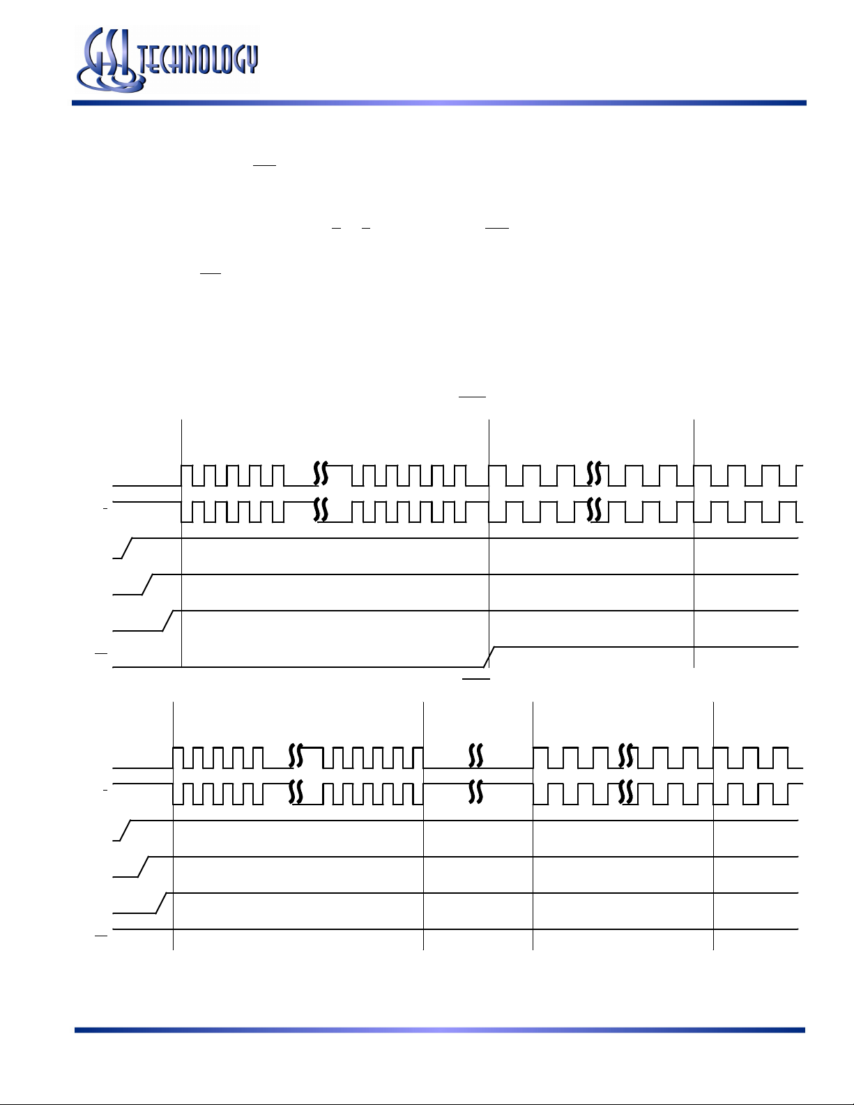
Power-Up Sequence for SigmaQuad-II SRAMs
SigmaQuad-II SRAMs must be powered-up in a specific sequence in order to avoid undefined operations.
Power-Up Sequence
1. Power-up and maintain Doff at low state.
1a. Apply VDD.
1b. Apply V
1c. Apply V
2. After power is achieved and clocks (K, K, C, C) are stablized, change Doff to high.
3. An additional 1024 clock cycles are required to lock the DLL after it has been enabled.
Note:
If you want to tie Doff high with an unstable clock, you must stop the clock for a minimum of 30 seconds to reset the DLL after the clocks become
stablized.
DLL Constraints
• The DLL synchronizes to either K or C clock. These clocks should have low phase jitter (t
• The DLL cannot operate at a frequency lower than 119 MHz.
• If the incoming clock is not stablized when DLL is enabled, the DLL may lock on the wrong frequency and cause undefined errors or failures during
the initial stage.
Power UP Interval Unstable Clocking Interval DLL Locking Interval (1024 Cycles) Normal Operation
.
DDQ
(may also be applied at the same time as V
REF
Power-Up Sequence (Doff controlled)
DDQ
).
on page 20).
KCVar
Preliminary
K
K
V
DD
V
DDQ
V
REF
Doff
Power-Up Sequence (Doff tied High)
Power UP Interval Unstable Clocking Interval Stop Clock Interval DLL Locking Interval (1024 Cycles) Normal Operation
K
K
V
DD
V
DDQ
30ns Min
V
REF
Doff
Note:
If the frequency is changed, DLL reset is required. After reset, a minimum of 1024 cycles is required for DLL lock.
Rev: 1.01 9/2005 8/37 © 2005, GSI Technology
Specifications cited are subject to change without notice. For latest documentation see http://www.gsitechnology.com.

Preliminary
GS8662R08/09/18/36E-333/300/250/200/167
Special Functions
Byte Write and Nybble Write Control
Byte Write Enable pins are sampled at the same time that Data In is sampled. A high on the Byte Write Enable pin associated with
a particular byte (e.g.,
stored at the current address at that byte location undisturbed. Any or all of the Byte Write Enable pins may be driven high or low
during the data in sample times in a write sequence.
Each write enable command and write address loaded into the RAM provides the base address for a 4 beat data transfer. The x18
version of the RAM, for example, may write 72 bits in association with each address loaded. Any 9-bit byte may be masked in any
write sequence.
Nybble Write (4-bit) write control is implemented on the 8-bit-wide version of the device. For the x8 version of the device,
“Nybble Write Enable” and “
Example x18 RAM Write Sequence using Byte Write Enables
BW0 controls D0–D8 inputs) will inhibit the storage of that particular byte, leaving whatever data may be
NBx” may be substituted in all the discussion above.
Data In Sample
Time
Beat 1 0 1 Data In Don’t Care
Beat 2 1 0 Don’t Care Data In
Beat 3 0 0 Data In Data In
Beat 4 1 0 Don’t Care Data In
BW0 BW1 D0–D8 D9–D17
Resulting Write Operation
Byte 1
D0–D8
Written Unchanged Unchanged Written Written Written Unchanged Written
Output Register Control
SigmaCIO DDR-II SRAMs offer two mechanisms for controlling the output data registers. Typically, control is handled by the
Output Register Clock inputs, C and
of the output registers by allowing the user to delay driving data out as much as a few nanoseconds beyond the next rising edges of
the K and
RAM to function as a conventional pipelined read SRAM.
K clocks. If the C and C clock inputs isare tied high, the RAM reverts to K and K control of the outputs, allowing the
Byte 2
D9–D17
Beat 1 Beat 2 Beat 3 Beat 4
Byte 1
D0–D8
C. The Output Register Clock inputs can be used to make small phase adjustments in the firing
Byte 2
D9–D17
Byte 1
D0–D8
Byte 2
D9–D17
Byte 1
D0–D8
Byte 2
D9–D17
Rev: 1.01 9/2005 9/37 © 2005, GSI Technology
Specifications cited are subject to change without notice. For latest documentation see http://www.gsitechnology.com.
LD
LD
LD
LD
R/W
A0–A
Preliminary
GS8662R08/09/18/36E-333/300/250/200/167
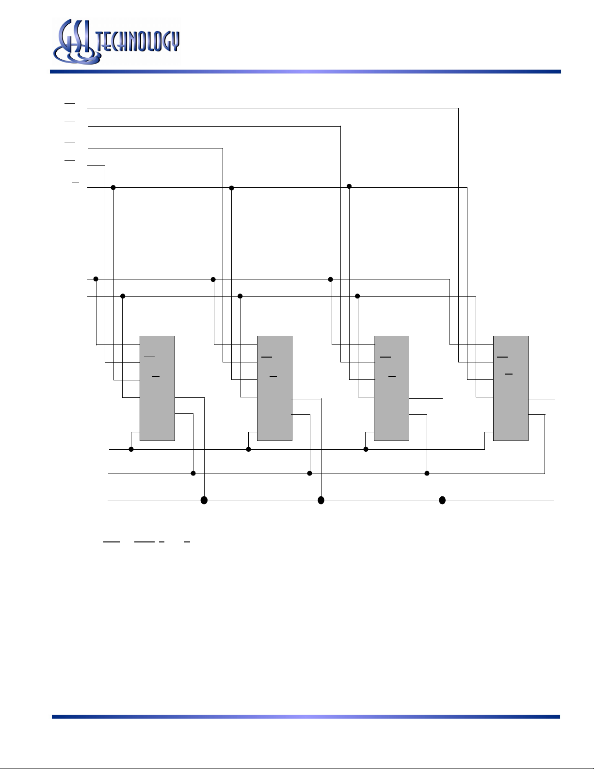
Example Four Bank Depth Expansion Schematic
3
2
1
0
n
K
C
DQ1–
CQ
Note:
For simplicity BWn
Bank 0
A
LD
R/W
CQ CQ CQ CQ
K
Bank 1 Bank 2
A
LD
A
LD
R/W R/W
K
K
Bank 3
A
LD
R/W
K
DQ DQ DQ DQ
CC CC
(or NWn), K, and C are not shown.
Rev: 1.01 9/2005 10/37 © 2005, GSI Technology
Specifications cited are subject to change without notice. For latest documentation see http://www.gsitechnology.com.
Preliminary
GS8662R08/09/18/36E-333/300/250/200/167
FLXDrive-II Output Driver Impedance Control
HSTL I/O SigmaCIO DDR-II SRAMs are supplied with programmable impedance output drivers. The ZQ pin must be connected
to V
via an external resistor, RQ, to allow the SRAM to monitor and adjust its output driver impedance. The value of RQ must be
SS
5X the value of the desired RAM output impedance. The allowable range of RQ to guarantee impedance matching continuously is
between 150Ω and 300Ω. Periodic readjustment of the output driver impedance is necessary as the impedance is affected by drifts
in supply voltage and temperature. The SRAM’s output impedance circuitry compensates for drifts in supply voltage and
temperature. A clock cycle counter periodically triggers an impedance evaluation, resets and counts again. Each impedance
evaluation may move the output driver impedance level one step at a time towards the optimum level. The output driver is
implemented with discrete binary weighted impedance steps. Updates of pull-down drive impedance occur whenever a driver is
producing a “1” or is High-Z. Pull-up drive impedance is updated when a driver is producing a “0” or is High-Z.
Common I/O SigmaCIO DDR-II B4 SRAM Truth Table
DQ
K
n
↑ 1 X Hi-Z Hi-Z Hi-Z Hi-Z Deselect
LD R/W
Operation
A + 0 A + 1 A + 2 A + 3
↑ 0 0 D@K
↑ 0 1
Note:
Q is controlled by K clocks if C clocks are not used.
Q@K
or
C
n+1
n+1
n+1
D@K
Q@K
or
C
n+2
n+1
n+2
D@K
Q@K
or
C
n+2
n+2
n+2
D@K
Q@K
or
C
n+3
n+2
n+3
Write
Read
Rev: 1.01 9/2005 11/37 © 2005, GSI Technology
Specifications cited are subject to change without notice. For latest documentation see http://www.gsitechnology.com.
Preliminary
GS8662R08/09/18/36E-333/300/250/200/167
B4 Byte Write Clock Truth Table
BW BW BW BW Current Operation D D D D
K ↑
(t
n+1
T T T T
T F F F
F T F F
F F T F
F F F T
F F F F
Notes:
1. “1” = input “high”; “0” = input “low”; “X” = input “don’t care”; “T” = input “true”; “F” = input “false”.
2. If one or more BWn = 0, then BW = “T”, else BW = “F”.
K ↑
(t
)
n+1½
K ↑
)
(t
n+2
K ↑
)
(t
)
n+2½
Dx stored if BWn = 0 in all four data transfers
Dx stored if BWn = 0 in 1st data transfer only
Dx stored if BWn = 0 in 2nd data transfer only
Dx stored if BWn = 0 in 3rd data transfer only
Dx stored if BWn = 0 in 4th data transfer only
No Dx stored in any of the four data transfers
K ↑
(tn)
Write
Write
Write
Write
Write
Write Abort
K ↑
(t
n+1
D0 D2 D3 D4
D0 X X X
X D1 X X
X X D2 X
X X X D3
X X X X
K ↑
)
(t
n+1½
K ↑
)
(t
)
n+2
(t
K ↑
n+2½
)
*Assuming stable conditions, the RAM can achieve optimum impedance within 1024 cycles.
Rev: 1.01 9/2005 12/37 © 2005, GSI Technology
Specifications cited are subject to change without notice. For latest documentation see http://www.gsitechnology.com.
 Loading...