

GSI TECHNOLOGY GS842Z18AB-180, GS842Z18AB-166, GS842Z18AB-150, GS842Z18AB-100, GS842Z36AB-180 Service Manual
...
GS842Z18/36AB-180/166/150/100
119-Bump BGA
4Mb Pipelined and Flow Through
Commercial Temp
Industrial Temp
Synchronous NBT SRAMs
Features
• 256K x 18 and 128K x 36 configurations
• User configurable Pipeline and Flow Through mode
• NBT (No Bus Turn Around) functionality allows zero wait
read-write-read bus utilization
• Fully pin compatible with both pipelined and flow through
NtRAM™, NoBL™ and ZBT™ SRAMs
• Pin-compatible with 2M, 8M, and 16M devices
• 3.3 V +10%/–10% core power supply
• 2.5 V or 3.3 V I/O supply
• LBO pin for Linear or Interleave Burst mode
• Byte write operation (9-bit Bytes)
• 3 chip enable signals for easy depth expansion
• Clock Control, registered address, data, and control
• ZZ Pin for automatic power-down
• JEDEC-standard 119-bump BGA package
• RoHS-compliant package available
Functional Description
The GS842Z18/36AB is a 4Mbit Synchronous Static SRAM.
GSI's NBT SRAMs, like ZBT, NtRAM, NoBL or other
pipelined read/double late write or flow through read/single
late write SRAMs, allow utilization of all available bus
bandwidth by eliminating the need to insert deselect cycles
when the device is switched from read to write cycles.
180 MHz–100 MHz
3.3 V V
2.5 V and 3.3 V V
Because it is a synchronous device, address, data inputs, and
read/ write control inputs are captured on the rising edge of the
input clock. Burst order control (
rail for proper operation. Asynchronous inputs include the
sleep mode enable (ZZ) and Output Enable. Output Enable can
be used to override the synchronous control of the output
drivers and turn the RAM's output drivers off at any time.
Write cycles are internally self-timed and initiated by the rising
edge of the clock input. This feature eliminates complex offchip write pulse generation required by asynchronous SRAMs
and simplifies input signal timing.
The GS842Z18/36AT may be configured by the user to
operate in Pipeline or Flow Through mode. Operating as a
pipelined synchronous device, in addition to the rising-edgetriggered registers that capture input signals, the device
incorporates a rising-edge-triggered output register. For read
cycles, pipelined SRAM output data is temporarily stored by
the edge triggered output register during the access cycle and
then released to the output drivers at the next rising edge of
clock.
The GS842Z18/36AT is implemented with GSI's high
performance CMOS technology and is available in a JEDECstandard 119-bump BGA package.
LBO) must be tied to a power
DD
DDQ
Parameter Synopsis
–180 –166 –150 –100
Pipeline
3-1-1-1
Flow
Through
2-1-1-1
Rev: 1.03a 10/2006 1/31 © 2001, GSI Technology
Specifications cited are subject to change without notice. For latest documentation see http://www.gsitechnology.com.
tCycle
t
KQ
I
DD
t
KQ
tCycle
I
DD
5.5 ns
3.2 ns
335 mA
8 ns
9.1 ns
210 mA
6.0 ns
3.5 ns
310 mA
8.5 ns
10 ns
190 mA
6.6 ns
3.8 ns
280 mA
10 ns
12 ns
165 mA
10 ns
4.5 ns
190 mA
12 ns
15 ns
135 mA

GS842Z18/36AB-180/166/150/100
GS842Z18A Pad Out—119-Bump BGA—Top View (Packge B)
1234567
A V
DDQ
AANCAAV
DDQ
B NC E2 AADVA E3 NC
C NC A A V
D DQ
E NC DQ
F V
B NC V
B V
DDQ
NC V
SS
SS
SS
DD
ZQ V
E1 V
G V
AANC
DQPA NC
SS
SS
SS
NC DQA
DQA V
DDQ
G NC DQB BB NC NC NC DQA
H DQB NC V
J V
DDQ
V
DD
K NC DQB V
SS
NC V
SS
W V
DD
CK V
SS
NC V
SS
DQA NC
V
DD
DDQ
NC DQA
L DQB NC NC NC BA DQA NC
M V
DDQ
DQB V
N DQB NC V
P NC DQP
B V
R NC A LBO V
SS
SS
SS
CKE V
A1 V
A0 V
DD
SS
SS
SS
NC V
DDQ
DQA NC
NC DQA
FT ANC
T NC A A NC A A ZZ
U V
DDQ
TMS TDI TCK TDO NC V
DDQ
Rev: 1.03a 10/2006 2/31 © 2001, GSI Technology
Specifications cited are subject to change without notice. For latest documentation see http://www.gsitechnology.com.

GS842Z18/36AB-180/166/150/100
GS842Z36A Pad Out— 119-Bump BGA—Top View (Package B)
1234567
A V
DDQ
AANCA8 AV
DDQ
B NC E2 AADVA E3 NC
C NC A A V
D DQ
E DQC DQC V
F V
C DQPC V
DDQ
DQC V
SS
SS
SS
DD
ZQ V
E1 V
G V
AANC
DQPB DQB
SS
DQB DQB
SS
DQB V
SS
DDQ
G DQC DQC BC NC BB DQB DQB
H DQC DQC V
J V
DDQ
V
DD
K DQD DQD V
SS
NC V
SS
W V
DD
CK V
SS
NC V
SS
DQB DQB
V
DD
DDQ
DQA DQA
L DQD DQD BD NC BA DQA DQA
M V
DDQ
N DQD DQD V
P DQD DQPD V
R NC A LBO V
DQD V
SS
SS
SS
CKE V
A1 V
A0 V
DD
DQA V
SS
SS
SS
DQA DQA
DQPA DQA
DDQ
FT ANC
T NC NC A A A NC ZZ
U V
DDQ
TMS TDI TCK TDO NC V
DDQ
Rev: 1.03a 10/2006 3/31 © 2001, GSI Technology
Specifications cited are subject to change without notice. For latest documentation see http://www.gsitechnology.com.
GS842Z18/36AB-180/166/150/100
GS842Z18/36A Pin Description
Symbol Type Description
A0, A1 I Address field LSBs and Address Counter Preset Inputs
An I Address Inputs
DQA
DQB
DQC
DQD
BA, BB, BC, BD I Byte Write Enable for DQA, DQB, DQC, DQA I/Os; active low ( x36 Version)
CK I Clock Input Signal; active high
CKE I Clock Input Buffer Enable; active low
W I Write Enable. Writes all enabled bytes; active low
E1 I Chip Enable; active low
G I Output Enable; active low
ADV I Burst address counter advance enable; active high
ZZ I Sleep Mode control; active high
FT I Flow Through or Pipeline mode; active low
LBO I Linear Burst Order mode; active low
ZQ I
NC — No Connect
TMS I Scan Test Mode Select
TDI I Scan Test Data In
TDO O Scan Test Data Out
TCK I Scan Test Clock
V
DD
V
SS
V
DDQ
CK I Clock Input Signal; active high
I/O Data Input and Output pins
I Chip Enable; active high
FLXDrive Output Impedance Control
(Low = Low Impedance [High Drive], High = High Impedance [Low Drive])
I Core power supply
I I/O and Core Ground
I Output driver power supply
Rev: 1.03a 10/2006 4/31 © 2001, GSI Technology
Specifications cited are subject to change without notice. For latest documentation see http://www.gsitechnology.com.
GS842Z18/36AB-180/166/150/100
Functional Details
Clocking
Deassertion of the Clock Enable (CKE) input blocks the Clock input from reaching the RAM's internal circuits. It may be used to
suspend RAM operations. Failure to observe Clock Enable set-up or hold requirements will result in erratic operation.
Pipelined Mode Read and Write Operations
All inputs (with the exception of Output Enable, Linear Burst Order and Sleep) are synchronized to rising clock edges. Single cycle
read and write operations must be initiated with the Advance/
activation is accomplished by asserting all three of the Chip Enable inputs (
inputs will deactivate the device.
Function W BA BB BC BD
Read H X X X X
Write Byte “a” L L H H H
Write Byte “b” L H L H H
Write Byte “c” L H H L H
Load pin (ADV) held low, in order to load the new address. Device
E1, E2, and E3). Deassertion of any one of the Enable
Write Byte “d” L H H H L
Write all Bytes L L L L L
Write Abort/NOP L H H H H
Read operation is initiated when the following conditions are satisfied at the rising edge of clock: CKE is asserted low, all three
chip enables (
presented to the address inputs is latched in to address register and presented to the memory core and control logic. The control
logic determines that a read access is in progress and allows the requested data to propagate to the input of the output register. At
the next rising edge of clock the read data is allowed to propagate through the output register and onto the Output pins.
Write operation occurs when the RAM is selected, CKE is active and the write input is sampled low at the rising edge of clock. The
Byte Write Enable inputs (
with no Byte Write inputs active is a no-op cycle. The Pipelined NBT SRAM provides double late write functionality, matching the
write command versus data pipeline length (2 cycles) to the read command versus data pipeline length (2 cycles). At the first rising
edge of clock, Enable, Write, Byte Write(s), and Address are registered. The Data In associated with that address is required at the
third rising edge of clock.
Flow through Mode Read and Write Operations
Operation of the RAM in Flow Through mode is very similar to operations in Pipeline mode. Activation of a read cycle and the use
of the Burst Address Counter is identical. In Flow Through mode the device may begin driving out new data immediately after new
address are clocked into the RAM, rather than holding new data until the following (second) clock edge. Therefore, in Flow
Through mode the read pipeline is one cycle shorter than in Pipeline mode.
E1, E2, and E3) are active, the write enable input signal W is deasserted high, and ADV is asserted low. The address
BA, BB, BC, and BD) determine which bytes will be written. All or none may be activated. A write cycle
Write operations are initiated in the same way as well, but differ in that the write pipeline is one cycle shorter as well, preserving
the ability to turn the bus from reads to writes without inserting any dead cycles. While the pipelined NBT RAMs implement a
double late write protocol, in Flow Through mode a single late write protocol mode is observed. Therefore, in Flow Through mode,
address and control are registered on the first rising edge of clock and data in is required at the data input pins at the second rising
edge of clock.
Rev: 1.03a 10/2006 5/31 © 2001, GSI Technology
Specifications cited are subject to change without notice. For latest documentation see http://www.gsitechnology.com.
GS842Z18/36AB-180/166/150/100
Synchronous Truth Table
Operation Type Address CK CKE ADV W Bx E1 E2 E3 G ZZ DQ Notes
Read Cycle, Begin Burst R External L-H L L H X L H L L L Q
Read Cycle, Continue Burst B Next L-H L H X X X X X L L Q 1,10
NOP/Read, Begin Burst R External L-H L L H X L H L H L High-Z 2
Dummy Read, Continue Burst B Next L-H L H X X X X X H L High-Z 1,2,10
Write Cycle, Begin Burst W External L-H L L L L L H L X L D 3
Write Cycle, Continue Burst B Next L-H L H X L X X X X L D 1,3,10
Write Abort, Continue Burst B Next L-H L H X H X X X X L High-Z 1,2,3,10
Deselect Cycle, Power Down D None L-H L L X X H X X X L High-Z
Deselect Cycle, Power Down D None L-H L L X X X X H X L High-Z
Deselect Cycle, Power Down D None L-H L L X X X L X X L High-Z
Deselect Cycle D None L-H L L L H L H L X L High-Z
Deselect Cycle, Continue D None L-H L H X X X X X X L High-Z 1
Sleep Mode None X X X X X X X X X H High-Z
Clock Edge Ignore, Stall Current L-H H X X X X X X X L - 4
Notes:
1. Continue Burst cycles, whether read or write, use the same control inputs. A Deselect continue cycle can only be entered into if a Deselect cycle is executed first.
2. Dummy Read and Write abort can be considered NOPs because the SRAM performs no operation. A Write abort occurs when the W
pin is sampled low but no Byte Write pins are active so no write operation is performed.
3. G can be wired low to minimize the number of control signals provided to the SRAM. Output drivers will automatically turn off during
write cycles.
4. If CKE High occurs during a pipelined read cycle, the DQ bus will remain active (Low Z). If CKE High occurs during a write cycle, the bus
will remain in High Z.
5. X = Don’t Care; H = Logic High; L = Logic Low; Bx = High = All Byte Write signals are high; Bx = Low = One or more Byte/Write
signals are Low
6. All inputs, except G and ZZ must meet setup and hold times of rising clock edge.
7. Wait states can be inserted by setting CKE high.
8. This device contains circuitry that ensures all outputs are in High Z during power-up.
9. A 2-bit burst counter is incorporated.
10. The address counter is incriminated for all Burst continue cycles.
1
Rev: 1.03a 10/2006 6/31 © 2001, GSI Technology
Specifications cited are subject to change without notice. For latest documentation see http://www.gsitechnology.com.
GS842Z18/36AB-180/166/150/100
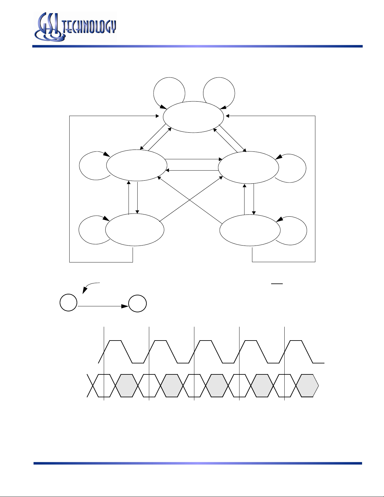
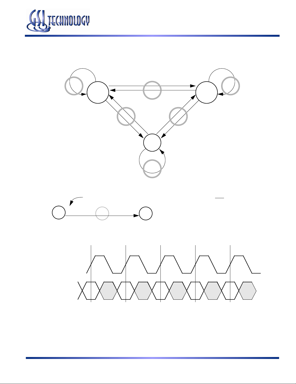
Pipelined and Flow Through Read-Write Control State Diagram
D
B
Deselect
R
D
W
New Read New Write
R
B
R
W
W
R
R
Burst Read Burst Write
B
Key Notes
ƒ
Current State (n)
Input Command Code
Transition
Next State (n+1)
1. The Hold command (CKE Low) is not
shown because it prevents any state change.
2. W, R, B, and D represent input command
codes as indicated in the Synchronous Truth Table.
D
W
B
W
B
DD
n n+1 n+2 n+3
Clock (CK)
Command
Current State Next State
ƒ
ƒƒƒ
Current State and Next State Definition for Pipelined and Flow Through Read/Write Control State Diagram
Rev: 1.03a 10/2006 7/31 © 2001, GSI Technology
Specifications cited are subject to change without notice. For latest documentation see http://www.gsitechnology.com.
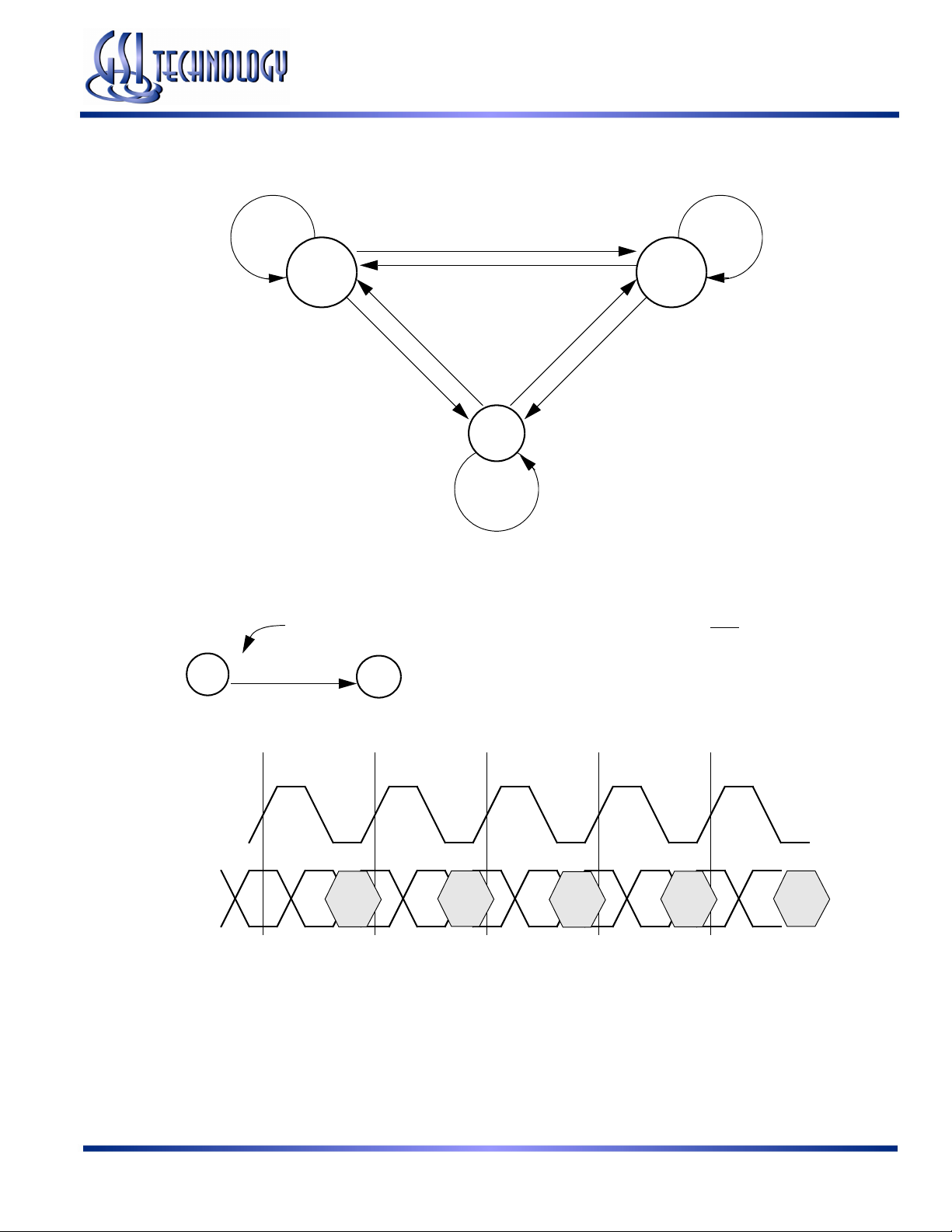
Pipeline Mode Data I/O State Diagram
GS842Z18/36AB-180/166/150/100
Intermediate Intermediate
Key
ƒ
Transition
Current State (n) Next State (n+2)
W
B
High Z
(Data In)
Input Command Code
R
D
Intermediate
Transition
Intermediate State (N+1)
Intermediate
W
High Z
B
D
Intermediate
R
B
Data Out
W
(Q Valid)
Intermediate
R
D
Notes
1. The Hold command (CKE Low) is not
shown because it prevents any state change.
2. W, R, B, and D represent input command
codes as indicated in the Truth Tables.
n n+1 n+2 n+3
Clock (CK)
Command
Current State
ƒ
ƒƒƒ
Intermediate
Next State
State
Current State and Next State Definition for Pipeline Mode Data I/O State Diagram
Rev: 1.03a 10/2006 8/31 © 2001, GSI Technology
Specifications cited are subject to change without notice. For latest documentation see http://www.gsitechnology.com.
GS842Z18/36AB-180/166/150/100
Flow Through Mode Data I/O State Diagram
W
B
High Z
(Data In)
R
D
W
R
High Z
B
D
R
B
Data Out
W
(Q Valid)
D
Key Notes
ƒ
Current State (n)
Clock (CK)
Command
Input Command Code
Transition
Next State (n+1)
n n+1 n+2 n+3
ƒ
Current State Next State
1. The Hold command (CKE Low) is not
shown because it prevents any state change.
2. W, R, B, and D represent input command
codes as indicated in the Truth Tables.
ƒƒƒ
Current State and Next State Definition for: Pipelined and Flow Through Read Write Control State Diagram
Rev: 1.03a 10/2006 9/31 © 2001, GSI Technology
Specifications cited are subject to change without notice. For latest documentation see http://www.gsitechnology.com.
GS842Z18/36AB-180/166/150/100
Burst Cycles
Although NBT RAMs are designed to sustain 100% bus bandwidth by eliminating turnaround cycle when there is transition from
Read to Write, multiple back-to-back reads or writes may also be performed. NBT SRAMs provide an on-chip burst address
generator that can be utilized, if desired, to further simplify burst read or write implementations. The ADV control pin, when
driven high, commands the SRAM to advance the internal address counter and use the counter generated address to read or write
the SRAM. The starting address for the first cycle in a burst cycle series is loaded into the SRAM by driving the ADV pin low, into
Load mode.
Burst Order
The burst address counter wraps around to its initial state after four addresses (the loaded address and three more) have been
accessed. The burst sequence is determined by the state of the Linear Burst Order pin (
sequence is selected. When the RAM is installed with the LBO pin tied high, interleaved burst sequence is selected. See the tables
below for details.
FLXDrive™
The ZQ pin allows selection between NBT RAM nominal drive strength (ZQ low) for multi-drop bus applications and low drive
strength (ZQ floating or high) point-to-point applications. See the Output Driver Characteristics chart for details.
Mode Pin Functions
Mode Name Pin Name State Function
Burst Order Control LBO
Output Register Control FT
Power Down Control ZZ
Single/Dual Cycle Deselect Control SCD
FLXDrive Output Impedance Control ZQ
9th Bit Enable PE
Note:
There is a are pull-up devices on the ZQ, SCD, and FT pins and a pull-down device on the ZZ pin, so thosethis input pins can be
unconnected and the chip will operate in the default states as specified in the above tables.
L Linear Burst
H Interleaved Burst
L Flow Through
H or NC Pipeline
L or NC Active
H
L Dual Cycle Deselect
H or NC Single Cycle Deselect
L High Drive (Low Impedance)
H or NC Low Drive (High Impedance)
L or NC Activate DQPx I/Os (x18/x3672 mode)
H Deactivate DQPx I/Os (x16/x3272 mode)
LBO). When this pin is low, a linear burst
Standby, IDD = I
SB
Rev: 1.03a 10/2006 10/31 © 2001, GSI Technology
Specifications cited are subject to change without notice. For latest documentation see http://www.gsitechnology.com.
 Loading...