

Datasheet GS70328SJ-15I, GS70328SJ-15, GS70328SJ-12I, GS70328SJ-12, GS70328SJ-10 Datasheet (GSI)
...
GS70328SJ/TS
SOJ, TSOP
32K x 8
Commercial Temp
Industrial Temp
256Kb Asynchronous SRAM
Features
• Fast access time: 7, 8, 10, 12, 15 ns
• 75/65/50/50/50 mA at max cycle rate
• Single 3.3 V ± 0.3 V power supply
• All inputs and outputs are TTL-compatible
• Fully static operation
• Industrial Temperature Option: –40° to 85°C
• Package line up
SJ: 300 mil, 28-pin SOJ package
TS: 8 mm x 13.4 mm, 28-pin TSOP Type I package
Description
The GS70328 is a high speed CMOS static RAM organized as
32,763 words by 8 bits. Static design eliminates the need for
external clocks or timing strobes. The GS70328 operates on a
single 3.3 V power supply, and all inputs and outputs are TTLcompatible. The GS70328 is available in 300 mil, 28-pin SOJ
and 8 x 13.4 mm
2
, 28-pin TSOP Type-I packages.
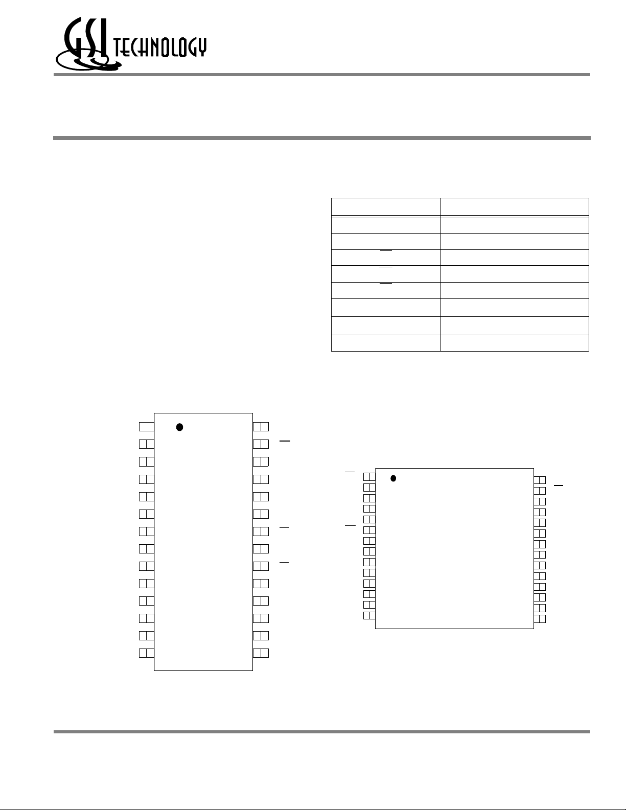
1
2
3
4
5
6
28-pin
7
300 mil
8
9
10
11
12
13
14
SOJ
DQ
DQ
DQ
V
14
A
A
12
A
7
A
6
A
5
A
4
A
3
A
2
A
1
A
0
1
2
3
SS
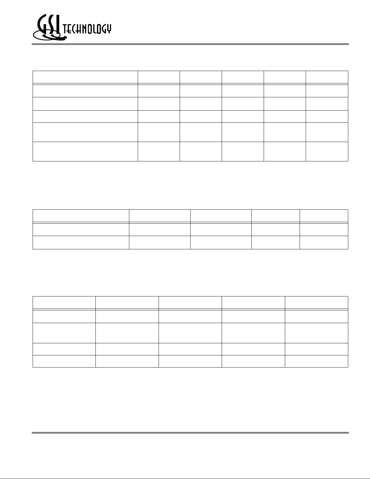
Pin Configuration
28
27
26
25
24
23
22
21
20
19
18
17
16
15
V
WE
A
A
A
A
OE
A
CE
DQ
DQ
DQ
DQ
DQ
DD
13
8
9
11
10
8
7
6
5
4
Pin Descriptions
Symbol Description
A0–A
DQ
Top view
OE
A
11
9
A
A
8
A
13
WE
V
DD
A
14
A
12
A
7
A
6
A
5
A
4
A
3
7, 8, 10, 12, 15 ns
Corner VDD and V
14
1–DQ8 Data input/output
CE
WE
OE
V
DD
V
SS
NC No connect
1
2
3
4
5
6
7
8
9
10
11
12
13
14
28- pin
8 x 13.4 TSOP I
Address input
Chip enable input
Write enable input
Output enable input
+3.3 V power supply
Ground
28
27
26
25
24
23
22
21
20
19
18
17
16
15
3.3 V V
10
A
CE
8
DQ
DQ
7
DQ
6
DQ
5
DQ
4
V
SS
DQ
3
DQ
2
DQ
1
A
0
A
1
A
2
DD
SS
Rev: 1.10 10/2002 1/12 © 1999, Giga Semiconductor, Inc.
Specifications cited are subject to change without notice. For latest documentation see http://www.gsitechnology.com.

Block Diagram
Truth Table
A
A
CE
WE
OE
GS70328SJ/TS
0
Address
Input
Buffer
14
Control
Row
Decoder
Memory Array
Column
Decoder
I/O Buffer
DQ
1
DQ
8
CE OE WE DQ1 to DQ
8
H X X Not Selected ISB1, ISB
L L H Read
LX L Write
LH H High Z
Note: X: “H” or “L”
Absolute Maximum Ratings
Parameter Symbol Rating Unit
Supply Voltage V
Input Voltage V
Output Voltage V
Allowable power dissipation PD 0.7 W
Storage temperature T
DD
IN
OUT
STG –55 to 150
–0.5 to +4.6 V
–0.5 to V
DD
(≤ 4.6 V max.)
–0.5 to VDD + 0.5
(≤ 4.6 V max.)
+ 0.5
V
V
o
C
VDD Current
2
DD
I
Note:
Permanent device damage may occur if Absolute Maximum Ratings are exceeded. Functional operation shall be restricted to Recommended
Operating Conditions. Exposure to higher than recommended voltages for extended periods of time could affect device reliability.
Rev: 1.10 10/2002 2/12 © 1999, Giga Semiconductor, Inc.
Specifications cited are subject to change without notice. For latest documentation see http://www.gsitechnology.com.
Recommended Operating Conditions
Parameter Symbol Minimum Typical Maximum Unit
GS70328SJ/TS
Supply Voltage for -7/8/10/12
Input High Voltage V
Input Low Voltage V
Ambient Temperature,
Commercial Range
Ambient Temperature,
Industrial Range
V
DD
IH
IL
T
Ac
I
T
A
3.0 3.3 3.6 V
2.0 —
–0.3 — 0.8 V
0—70
–40 — 85
Notes:
1. Input overshoot voltage should be less than V
+2 V and not exceed 20 ns.
DD
2. Input undershoot voltage should be greater than –2 V and not exceed 20 ns.
Capacitance
Parameter Symbol Test Condition Maximum Unit
C
C
OUT
IN
Input Capacitance
Output Capacitance
Notes:
1. Tested at T
A = 25°C, f = 1 MHz
2. These parameters are sampled and are not 100% tested.
V
V
IN
OUT
= 0 V
= 0 V
V
DD
+ 0.3
V
o
C
o
C
5pF
7pF
DC I/O Pin Characteristics
Parameter Symbol Test Conditions Min Max
V
Input Leakage Current I
Output Leakage Current I
Output High Voltage V
Output Low Voltage V
IL
LO
OH
OL ILO = +4 mA — 0.4 V
Rev: 1.10 10/2002 3/12 © 1999, Giga Semiconductor, Inc.
Specifications cited are subject to change without notice. For latest documentation see http://www.gsitechnology.com.
= 0 to V
IN
DD
Output High Z
V
= 0 to V
OUT
OH
I
DD
= –4 mA 2.4 V —
–1uA 1uA
–1uA 1uA

Power Supply Currents
Parameter Symbol Test Conditions
≤ VIL
CE
Operating
Supply
Current
Standby
Current
Standby
Current
IDD
ISB1
ISB2
All other inputs
≥ VIH or ≤ VIL
Min. cycle time
IOUT = 0 mA
≥ VIH
CE
All other inputs
≥ VIH or ≤VIL
Min. cycle time
CE
≥ V
– 0.2 V
DD
All other inputs
– 0.2 V or
≥ V
DD
≤ 0.2 V
GS70328SJ/TS
0 to 70°C -40 to 85°C
7 ns 8 ns 10 ns 12 ns 15 ns 7 ns 8 ns 10 ns 12 ns 15 ns
75 mA 65 mA 50 mA 50 mA 50 mA 80 mA 70 mA 55 mA 55 mA 55 mA
35 mA 30 mA 25 mA 25 mA 25 mA 40 mA 35 mA 30 mA 30 mA 30 mA
1 mA 2 mA
AC Test Conditions
Parameter Conditions
Input high level VIH = 2.4 V
Input low level V
Input rise time tr = 1 V/ns
Input fall time tf = 1 V/ns
Input reference level 1.4 V
Output reference level 1.4 V
Output load Fig. 1& 2
Notes:
1. Include scope and jig capacitance
2. Test conditions as specified with output loading as shown in Fig. 1 unless otherwise noted
3. Output load 2 for t
LZ, tHZ, tOLZ and tOHZ
IL
= 0.4 V
DQ
Output Load 1
VT = 1.4 V
Output Load 2
DQ
5pF
1
50Ω
3.3 V
589Ω
434Ω
30pF
1
Rev: 1.10 10/2002 4/12 © 1999, Giga Semiconductor, Inc.
Specifications cited are subject to change without notice. For latest documentation see http://www.gsitechnology.com.

AC Characteristics
Read Cycle
Parameter Symbol
GS70328SJ/TS
-7 -8 -10 -12 -15
Unit
Min Max Min Max Min Max Min Max Min Max
Read cycle time t
Address access time t
Chip enable access time (CE
Output enable to output valid (OE
)tAC —7—8—10—12—15ns
)tOE—3.5—4—5 — 6 — 7ns
Output hold from address change t
Chip enable to output in low Z (CE
Output enable to output in low Z (OE
Chip disable to output in High Z (CE
Output disable to output in High Z (OE
)
)
)
)
t
t
OLZ
t
OHZ
t
RC
AA
OH
*
LZ
*
*
HZ
*
* These parameters are sampled and are not 100% tested
7—8—10—12—15—ns
—7—8—10—12—15ns
2—2—2— 3 — 3 —ns
2—2—2— 3 — 3 —ns
0—0—0— 0 — 0 —ns
—3.5—4—5 — 6 — 7ns
—3—3.5—4 — 5 — 6ns
Rev: 1.10 10/2002 5/12 © 1999, Giga Semiconductor, Inc.
Specifications cited are subject to change without notice. For latest documentation see http://www.gsitechnology.com.

GS70328SJ/TS
Read Cycle 1: CE = OE = VIL, WE = V
Address
Data Out Previous Data Data valid
Read Cycle 2: WE = V
IH
Address
CE
OE
Data Out
IH
High impedance
RC
t
AA
t
OH
t
RC
t
tAA
tAC
HZ
tLZ
tOLZ
tOE
D
t
tOHZ
ATA VALID
Rev: 1.10 10/2002 6/12 © 1999, Giga Semiconductor, Inc.
Specifications cited are subject to change without notice. For latest documentation see http://www.gsitechnology.com.

Write Cycle
GS70328SJ/TS
Parameter Symbol
Write cycle time tWC 7 — 8 — 10 — 12 — 15 — ns
Address valid to end of write tAW 5 — 5.5 — 7 — 10 — 13 — ns
Chip enable to end of write tCW 5 — 5.5 — 7 — 10 — 13 — ns
Data set up time tDW 3.5 — 4 — 5 — 7 — 10 — ns
Data hold time tDH 0 — 0 — 0 — 0 — 0 — ns
Write pulse width tWP 5 — 5.5 — 7 — 10 — 13 — ns
Address set up time tAS 0 — 0 — 0 — 0 — 0 — ns
Write recovery time (WE
Write recovery time (CE
Output Low Z from end of write
Write to output in High Z
* These parameters are sampled and are not 100% tested
) tWR 0—0—0— 0 — 0 —ns
) tWR1 0—0—0— 0 — 0 —ns
*
tWLZ
*
tWHZ
-7 -8 -10 -12 -15
Min Max Min Max Min Max Min Max Min Max
2—2—2— 3 — 3 —ns
—3—3.5—4 — 5 — 5ns
Unit
Rev: 1.10 10/2002 7/12 © 1999, Giga Semiconductor, Inc.
Specifications cited are subject to change without notice. For latest documentation see http://www.gsitechnology.com.

Write Cycle 1: WE control
Address
GS70328SJ/TS
WC
t
CE
WE
Data In
Data Out
Write Cycle 2: CE control
Address
OE
CE
OE
tAW
tWR
tCW
AS
t
WP
t
DW
t
D
ATA VALID
DH
t
tWLZtWHZ
IGH IMPEDANCE
H
WC
t
tAW
AS
t
CW
t
tWR1
B
t
W
UB, LB
WP
t
WE
Data In
Data Out
DW
t
D
IGH IMPEDANCE
H
ATA VALID
DH
t
Rev: 1.10 10/2002 8/12 © 1999, Giga Semiconductor, Inc.
Specifications cited are subject to change without notice. For latest documentation see http://www.gsitechnology.com.

28-Pin SOJ, 300 mil
1
e
A2
A
A1
GS70328SJ/TS
Dimension in inch Dimension in mm
Symbol
L
D
c
A — — 0.148 — — 3.76
A1 0.025 — — 0.64 — —
A2 0.095 0.100 0.105 2.41 2.54 2.67
E
E
H
E
G
B 0.015 — 0.020 0.38 — 0.51
B1 0.026 0.028 0.032 0.66 0.71 0.81
A
c 0.008 0.010 0.012 0.20 0.25 0.30
D
E 0.295 0.300 0.305 7.49 7.62 7.75
e — 0.05 — — 1.27 —
y
B
B1
Detail A
HE 0.330 0.335 0.340 8.38 8.51 8.64
Θ
GE 0.255 0.265 0.275 6.48 6.73 6.985
L 0.082 — — 2.08 — —
y — — 0.004 — — 0.10
Θ
Notes:
1. Dimension D& E do not include interlead flash
2. Dimension B1 does not include dambar protrusion/intrusion
3. Controlling dimension: inches
min nom max min nom max
0.705 0.71 0.715 17.91 18.03 18.16
o
0
—
10
o
o
—
0
10
o
Rev: 1.10 10/2002 9/12 © 1999, Giga Semiconductor, Inc.
Specifications cited are subject to change without notice. For latest documentation see http://www.gsitechnology.com.

28-Pin TSOP-I, 8 mm x 13.4 mm
Q
A2
A1
E
D
D
1
e
e
B
y
y
28
A
1
A2
A
A1
GS70328SJ/TS
Dimension in inch Dimension in mm
c
L
c
E
E
D
H
H
A
L1
E
G
A
B
B1
Detail A
L
Detail A
Θ
Symbol
min nom max min nom max
A — — 0.047 — — 1.20
A1 0.002 — 0.006 0.05 — 0.15
A2 0.035 0.040 0.041 0.90 1.00 1.05
B 0.007 0.008 0.011 0.17 0.20 0.27
D — 0.465 — — 11.8 —
H
D
— .528 — — 13.4 —
c 0.004 0.006 0.008 0.10 0.15 0.21
E — 0.315 — — 8.00 —
e — 0.022 — — 0.55 —
L 0.020 0.024 0.028 0.50 0.60 0.70
L1 0.024 0.032 0.040 0.60 0.80 1.00
y — — 0.003 — — 0.08
Θ
o
0
—
o
5
o
0
—
o
5
Notes:
1. Dimension D& E do not include interlead flash
2. Dimension B1 does not include dambar protrusion/intrusion
3. Controlling dimension: inches
4. Profile tolerance zones for D and E do not include mold
protrusion. Allowable mold protrusion on E is 0.15 mm per side
and on D is 0.25 mm per side.
Rev: 1.10 10/2002 10/12 © 1999, Giga Semiconductor, Inc.
Specifications cited are subject to change without notice. For latest documentation see http://www.gsitechnology.com.

Ordering Information
GS70328SJ/TS
Part Number
*
Package Access Time Temp. Range Status
GS70328SJ-7 300-mil SOJ 7 ns Commercial
GS70328SJ-8 300-mil SOJ 8 ns Commercial
GS70328SJ-10 300-mil SOJ 10 ns Commercial
GS70328SJ-12 300-mil SOJ 12 ns Commercial
GS70328SJ-15 300-mil SOJ 15 ns Commercial
GS70328SJ-7I 300-mil SOJ 7 ns Industrial
GS70328SJ-8I 300-mil SOJ 8 ns Industrial
GS70328SJ-10I 300-mil SOJ 10 ns Industrial
GS70328SJ-12I 300-mil SOJ 12 ns Industrial
GS70328SJ-15I 300-mil SOJ 15 ns Industrial
GS70328TS-7
GS70328TS-8
GS70328TS-10
TSOP-I 8 x 13.4 mm
TSOP-I 8 x 13.4 mm
TSOP-I 8 x 13.4 mm
2
2
2
7 ns Commercial
8 ns Commercial
10 ns Commercial
GS70328TS-12
GS70328TS-15
GS70328TS-7I
GS70328TS-8I
GS70328TS-10I
GS70328TS-12I
GS70328TS-15I
*
Customers requiring delivery in Tape and Reel should add the character “T” to the end of the part number. For example: GS70328TP-8T
TSOP-I 8 x 13.4 mm
TSOP-I 8 x 13.4 mm
TSOP-I 8 x 13.4 mm
TSOP-I 8 x 13.4 mm
TSOP-I 8 x 13.4 mm
TSOP-I 8 x 13.4 mm
TSOP-I 8 x 13.4 mm
2
2
2
2
2
2
2
12 ns Commercial
15 ns Commercial
7 ns Industrial
8 ns Industrial
10 ns Industrial
12 ns Industrial
15 ns Industrial
Rev: 1.10 10/2002 11/12 © 1999, Giga Semiconductor, Inc.
Specifications cited are subject to change without notice. For latest documentation see http://www.gsitechnology.com.

Revision History
GS70328SJ/TS
Rev. Code: Old;
New
1.03 8/1999;
1.04 11/1999
GS70328Rev1.04 12/1999KRev
1.05 2/2000L
Rev 1.05 2/2000L; Rev1.06 6/2000 Content
Rev1.06; Rev1.07 Format/Content
70328_r1_07; 70328_r1_08 Content
70328_r1_08; 70328_r1_09 Content
70328_r1_09; 70328_r1_10 Content
Types of Changes
Format or Content
Content
Format/Content
Page #/Revisions/Reason
• Added 12ns speed bin information to 70328 datasheet.
• GSI Logo
• Nominal value for H
to 13.4
• Updated format to conform to Tech Pubs standards
• Corrected errors in both case diagrams
• Added 12 ns reference to Parameter column in
Recommended Operating Conditions table on page 3
• Added 15 ns references to entire document
• Removed 6 ns speed bin from entire document
on the TSOP-I 28-pin package changed
D
Rev: 1.10 10/2002 12/12 © 1999, Giga Semiconductor, Inc.
Specifications cited are subject to change without notice. For latest documentation see http://www.gsitechnology.com.
 Loading...