

GSI GS841E18AT-166I, GS841E18AT-150I, GS841E18AT-150, GS841E18AT-133I, GS841E18AT-133 Datasheet
...
Rev: 1.00 10/2001 1/29 © 2001, Giga Semiconductor, Inc.
Specifications cited are subject to change without notice. For latest documentation see http://www.gsitechnology.com.
Trademark Notice (if any) Trademark of Giga Semiconductor, Inc. (GSI Technology).
GS841E18AT/B-166/150/133/100
256K x 18 Sync
Cache Tag
166 MHz–100 MHz
8.5 ns–12 ns
3.3 V V
DD
3.3 V and 2.5 V I/O
TQFP, BGA
Commercial Temp
Industrial Temp
Features
• 3.3 V +10%/–5% core power supply, 2.5 V or 3.3 V I/O
supply
• Dual Cycle Deselect (DCD)
• Intergrated data comparator for Tag RAM application
• FT mode pin for flow through or pipeline operation
• LBO pin for Linear or Interleave (PentiumTM and X86) Burst
mode
• Synchronous address, data I/O, and control inputs
• Synchronous Data Enable (DE)
• Asynchronous Output Enable (OE)
• Asynchronous Match Output Enable (MOE)
• Byte Write (BWE) and Global Write (GW) operation
• Three chip enable signals for easy depth expansion
• Internal self-timed write cycle
• JTAG Test mode conforms to IEEE standard 1149.1
• JEDEC-standard 100-lead TQFP package and 119-BGA:
T:TQFP or B: BGA
Functional Description
The GS841E18A is a 256K x 18 high performance
synchronous DCD SRAM with integrated Tag RAM
comparator. A 2-bit burst counter is included to provide burst
interface with PentiumTM and other high performance CPUs. It
is designed to be used as a Cache Tag SRAM, as well as data
SRAM. Addresses, data IOs, match output, chip enables (CE1,
CE2, CE3), address control inputs (ADSP, ADSC, ADV), and
write control inputs (BW1, BW2, BWE, GW, DE) are
synchronous and are controlled by a positive-edge-triggered
clock (CLK).
Output Enable (OE), Match Output Enable, and power down
control (ZZ) are asynchronous. Burst can be initiated with
either ADSP or ADSC inputs. Subsequent burst addresses are
generated internally and are controlled by ADV. The burst
sequence is either interleave order (PentiumTM or x86) or
linear order, and is controlled by LBO.
Output registers and the Match output register are provided and
controlled by the FT mode pin (Pin 14). Through use of the FT
mode pin, I/O registers can be programmed to perform pipeline
or flow through operation. Flow Through mode reduces
latency.
Byte write operation is performed by using Byte Write Enable
(BWE) input combined with two individual byte write signals
BW1-2. In addition, Global Write (GW) is available for
writing all bytes at one time.
Compare cycles begin as a read cycle with output disabled so
that compare data can be loaded into the data input register.
The comparator compares the read data with the registered
input data and a match signal is generated. The match output
can be either in Pipeline or Flow Through modes controlled by
the FT signal.
Low power (Standby mode) is attained through the assertion of
the ZZ signal, or by stopping the clock (CLK). Memory data is
retained during Standby mode.
JTAG boundary scan interface is provided using IEEE
standard 1149.1 protocol. Four pins—Test Data In (TDI), Test
Data Out (TDO), Test Clock (TCK) and Test Mode Select
(TMS)—are used to perform JTAG function.
The GS841E18A operates on a 3.3 V power supply and all
inputs/outputs are 3.3 V- or 2.5 V-LVTTL-compatible.
Separate output (V
DDQ
) pins are used to allow both 3.3 V or
2.5 V IO interface.
Dual Cycle Deselect (DCD)
The GS841E18A is a DCD pipelines synchronous SRAM.
DCD SRAMs pipeline disable commands to the same degree
as read commands. DCD SRAMs hold the deselect command
for one full cycle and then begin turning off their outputs just
after the second rising edge of the clock.
* Pentium is a trademark of Intel Corp.
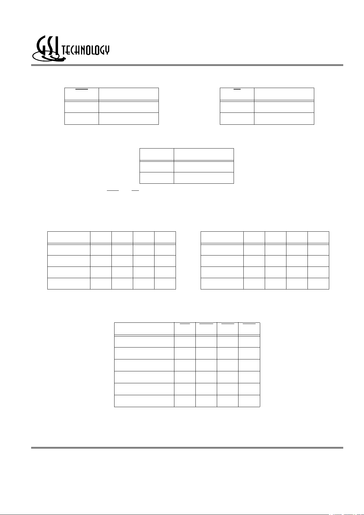
-166 -150 -133 -100
Pipeline
3-1-1-1
t
cycle
t
KQ
I
DD
6.0 ns
3.5 ns
310 mA
6.6 ns
3.8 ns
275 mA
7.5 ns
4.0 ns
250 mA
10 ns
4.5 ns
190 mA
Flow
Through
2-1-1-1
t
KQ
t
cycle
I
DD
8.5 ns
10 ns
190 mA
10 ns
10 ns
190 mA
11 ns
15 ns
140 mA
12 ns
15 ns
140 mA
Rev: 1.00 10/2001 2/29 © 2001, Giga Semiconductor, Inc.
Specifications cited are subject to change without notice. For latest documentation see http://www.gsitechnology.com.
GS841E18AT/B-166/150/130/100
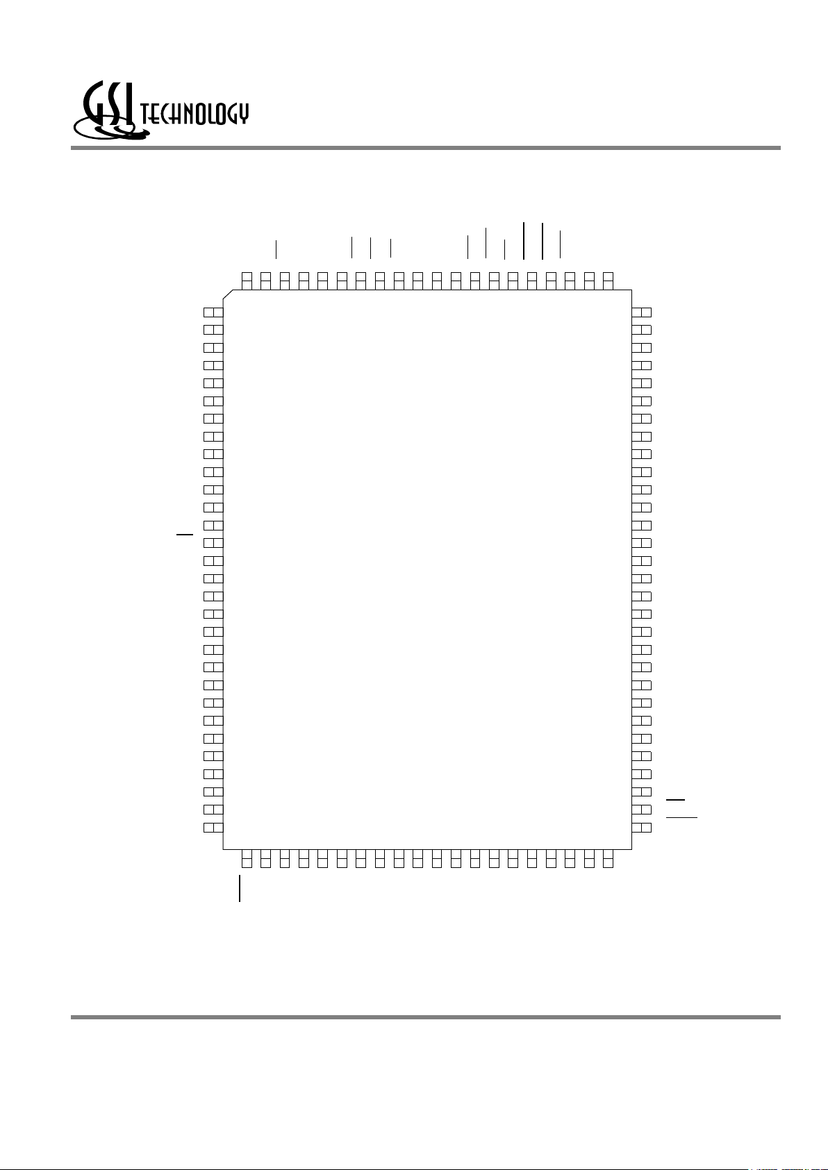
Pin Configuration
80
79
78
77
76
75
74
73
72
71
70
69
68
67
66
65
64
63
62
61
60
59
58
57
56
55
54
53
52
51
1
2
3
4
5
6
7
8
9
10
11
12
13
14
15
16
17
18
19
20
21
22
23
24
25
26
27
28
29
30
V
DDQ
V
SS
DQ9
DQ10
V
SS
V
DDQ
DQ11
DQ12
V
DD
NC
V
SS
DQ13
DQ14
V
DDQ
V
SS
DQ15
DQ16
DQP2
V
SS
V
DDQ
V
DDQ
V
SS
DQ8
DQ7
V
SS
VDDQ
DQ6
DQ5
V
SS
NC
V
DD
ZZ
DQ4
DQ3
V
DDQ
V
SS
DQ2
DQ1
V
SS
V
DDQ
LBO
A5
A4
A3
A2
A1
A0
TMS
TDI
V
SS
V
DD
TDO
TCK
A15
A14
A13
A12
A11
A17
A6
A7
CE1
CE2
NC
NC
BW2
BW1
CE3
CLK
GW
BWE
V
DD
V
SS
OE
ADSC
ADSP
ADVA8A9
A16
256K x 18
Top View
DQP1
A10
NC
NC
NC
NC
NC
DE
MATCH
MOE
NC
NC
NC
NC
NC
NC
NC
NC
NC
100 99 98 97 96 95 94 93 92 91 90 89 88 87 86 85 84 83 82 81
31 32 33 34 35 36 37 38 39 40 41 42 43 44 45 46 47 48 49 50
FT
Rev: 1.00 10/2001 3/29 © 2001, Giga Semiconductor, Inc.
Specifications cited are subject to change without notice. For latest documentation see http://www.gsitechnology.com.
GS841E18AT/B-166/150/130/100
841E18A PadOut
119-Bump BGA—Top View
1 2 3 4 5 6 7
A
V
DDQ
A6 A7 ADSP A8 A9 V
DDQ
B
NC E2 A4 ADSC A15 E3 NC
C
NC A5 A3 V
DD
A14 A16 NC
D
DQB1 NC V
SS
NC V
SS
DQP1 NC
E
NC DQB2 V
SS
E1 V
SS
NC DQA8
F
V
DDQ
NC V
SS
G V
SS
DQA7 V
DDQ
G
NC DQB3 BB ADV NC NC DQA6
H
DQB4 NC V
SS
GW V
SS
DQA5 NC
J
V
DDQ
V
DD
NC V
DD
NC V
DD
V
DDQ
K
NC DQB5 V
SS
CK V
SS
NC DQA4
L
DQB6 NC NC NC BA DQA3 NC
M
V
DDQ
DQB7 V
SS
BW V
SS
MATCH V
DDQ
N
DQB8 NC V
SS
A1 V
SS
DQA2 DE
P
NC DQP2 V
SS
A0 V
SS
MOE DQA1
R
NC A2 LBO V
DD
FT A13 NC
T
NC A10 A11 NC A12 A17 ZZ
U
V
DDQ
TMS TDI NC TDO TCK V
DDQ
Rev: 1.00 10/2001 4/29 © 2001, Giga Semiconductor, Inc.
Specifications cited are subject to change without notice. For latest documentation see http://www.gsitechnology.com.
GS841E18AT/B-166/150/130/100
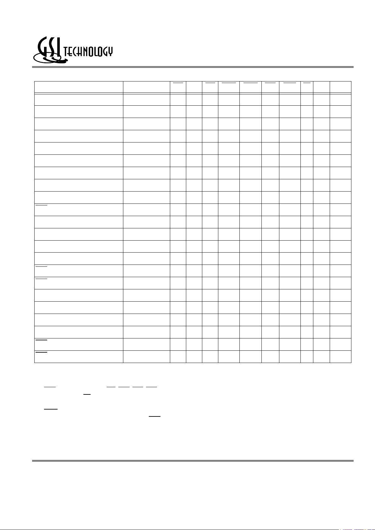
TQFP Pin Description
Pin Location Symbol Description
37, 36, 35, 34, 33, 32, 100, 99, 82, 81, 80, 48,
47, 46, 45, 44, 49, 50
A0–A17
Address Input Signals—Inputs are registered and must meet
setup and hold times, as specified on page 11.
89 CLK Clock Input Signal
87 BWE
Byte Write Enable Signal—The byte write enable signal
needs to be combined with one of the four byte write signals
for a write operation to occur.
93 BW1 Byte Write signal for data outputs 1 thru 8
94 BW2 Byte Write signal for data outputs 9 thru 16
88 GW Global Write Enable
92, 97, 98 CE1,CE2, CE3 Chip Enables
86 OE Output Enable
83 ADV Burst address advance
84, 85 ADSP, ADSC Address status signals
58, 59, 62 ,63, 68, 69, 72, 73, 8, 9, 12, 13, 18,
19, 22, 23
DQ1–DQ16 Data Input and Output pins
74, 24 DQP1–DQP2 Parity Input and Output pins
53 MATCH Match Output
51 MOE Match Output Enable
52 DE
Data Enable—Data input registers are updated only when DE
is active.
64 ZZ
Power down control—Application of ZZ will result in a low
standby power consumption.
14 FT Flow Through or Pipeline mode
31 LBO Linear Order Burst mode
38 TMS Test Mode Select
39 TDI Test Data In
42 TDO Test Data Out
43 TCK Test Clock
15, 41, 65, 91
V
DD
3.3 V power supply
5,10,17, 21, 26, 40, 55, 60, 67, 71,
76, 90
V
SS
Ground
4, 11, 20, 27, 54, 61, 70, 77
V
DDQ
2.5 V/3.3 V output power supply
1, 2, 3, 6, 7, 16, 25, 28, 29, 30,56, 57, 66, 75,
78, 79, 95, 96
NC No Connect

Rev: 1.00 10/2001 5/29 © 2001, Giga Semiconductor, Inc.
Specifications cited are subject to change without notice. For latest documentation see http://www.gsitechnology.com.
GS841E18AT/B-166/150/130/100
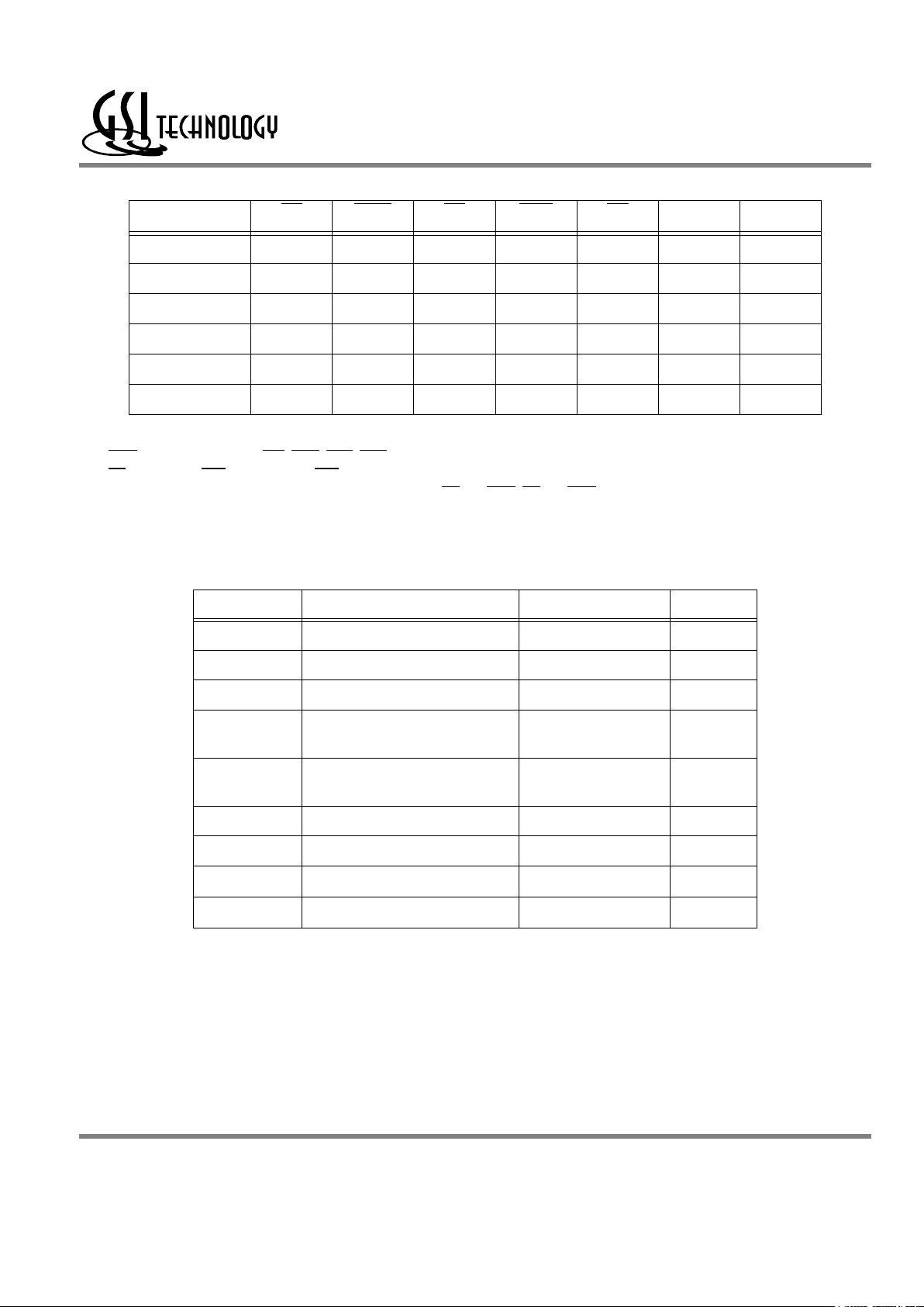
PBGA Pin Description
Pin Location Symbol Description
P4, N4, R2, C3, B3, C2, A2, A3, A5, A6, T6, C5,
R6, T5, T2, T3, B5, C6
A0–A17
Address Input Signals—Inputs are registered and must meet
setup and hold times, as specified on page 11.
K4 CLK Clock Input Signal
M4 BWE
Byte Write Enable Signal—The byte write enable signal needs to
be combined with one of the four byte write signals for a write
operation to occur.
L5 BW1 Byte Write signal for data outputs 1 thru 8
G3 BW2 Byte Write signal for data outputs 9 thru 16
H4 GW Global Write Enable
E4, B2, B6 CE1,CE2, CE3 Chip Enables
F4 OE Output Enable
G4 ADV Burst address advance
A4, B4 ADSP, ADSC Address status signals
P7, N6, L6, K7, H6, G7, F6, E7, D1, E2, G2, H1,
K2, L1, M2, N1
DQ1–DQ16 Data Input and Output pins
D6, P2 DQP1–DQP2 Parity Input and Output pins
M6 MATCH Match Output
P6 MOE Match Output Enable
N7 DE
Data Enable—Data input registers are updated only when DE is
active.
T7 ZZ
Power down control—Application of ZZ will result in a low
standby power consumption.
R5 FT Flow Through or Pipeline mode
R3 LBO Linear Order Burst mode
U2 TMS Test Mode Select
U3 TDI Test Data In
U5 TDO Test Data Out
U4 TCK Test Clock
C4, J2, J4, J6, R4
V
DD
3.3 V power supply
D3, D5, E3, E5, F3, F5, H3, H5, K3, K5, M3, M5,
N3, N5, P3, P5
V
SS
Ground
A1, A7, F1, F7, J1, J7, M1, M7, U1, U7
V
DDQ
2.5 V/3.3 V output power supply
B1, B7, C1, C7, D2, D4, D7, E1, E6, F2, G1, G5,
G6, H2, H7, J3, J5, K1, K6, L2, L3, L4, L7, N2,
P1, RR1, R7, T1, T4, U6
NC No Connect
Rev: 1.00 10/2001 6/29 © 2001, Giga Semiconductor, Inc.
Specifications cited are subject to change without notice. For latest documentation see http://www.gsitechnology.com.
GS841E18AT/B-166/150/130/100
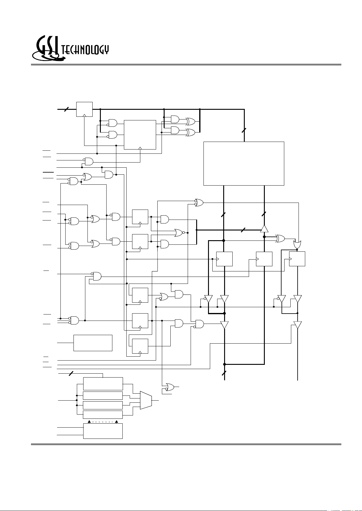
Functional Block Diagram
A1
A0
A0
A1
D0
D1
Q1
Q0
BINARY
COUNTER
Load
D Q
REGISTER
D Q
Register
D Q
Register
D Q
Register
D Q
Register
D Q
Register
D Q
Register
DQ
Register
A0-17
LBO
ADV
CLK
ADSC
ADSP
GW
BWE
BW1
BW2
CE1
CE2
CE3
FT
DQ1-16
OE
ZZ
Powerdown
Control
256K X 18
Memory
Array
18
18
18
18
2
18
A
Q D
DQP1-2
DE
D Q
Register
Match
TAP
Controller
Instruction Reg.
ID Reg.
Bypass Reg
Boundary Scan
Registers
54
TCK
TMS
TDI
A, DQ,
Control
TDO
MOE
always (Ø)
Rev: 1.00 10/2001 7/29 © 2001, Giga Semiconductor, Inc.
Specifications cited are subject to change without notice. For latest documentation see http://www.gsitechnology.com.
GS841E18AT/B-166/150/130/100
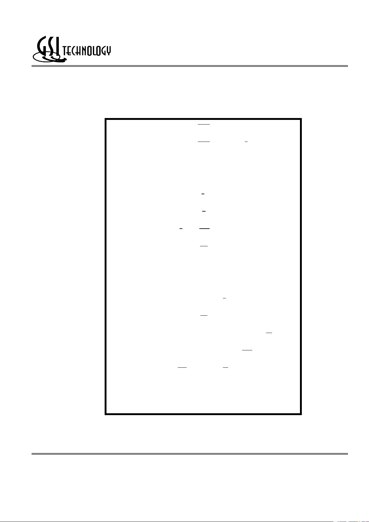
Mode Pin Function
LBO Function
L Linear Burst
H or NC Interleaved Burst
FT Function
L Flow Through
H or NC Pipeline
Power Down Control
Note:
There are pull up devices on LBO and FT pins and pull down device on ZZ pin, so those input pins can be unconnected
and the chip will operate in the default states as specified in the above tables.
ZZ Function
L or NC Active
H Standby, IDD = ISB
Linear Burst Sequence
A[1:0] A[1:0] A[1:0] A[1:0]
1st address 00 01 10 11
2nd address 01 10 11 00
3rd address 10 11 00 01
4th address 11 00 01 10
Interleaved Burst Sequence
A[1:0] A[1:0] A[1:0] A[1:0]
1st address 00 01 10 11
2nd address 01 00 11 10
3rd address 10 11 00 01
4th address 11 10 01 00
Byte Write Function
Note: H = logic high, L = logic low, NC = no connect
Function GW BWE BW1 BW2
Read H H X X
Read H L H H
Write all bytes L X X X
Write all bytes H L L L
Write byte 1 H L L H
Write byte 2 H L H L
Rev: 1.00 10/2001 8/29 © 2001, Giga Semiconductor, Inc.
Specifications cited are subject to change without notice. For latest documentation see http://www.gsitechnology.com.
GS841E18AT/B-166/150/130/100
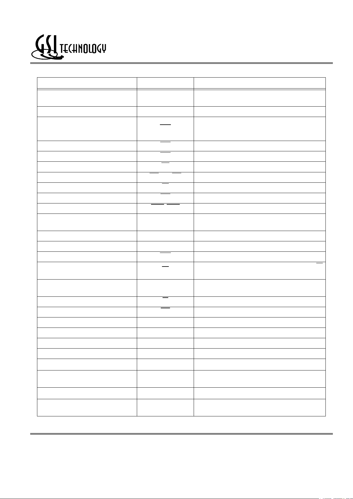
Synchronous Truth Table
Notes:
1. X means “don’t care,” H means “logic high,” L means “logic low.”
2. Write is the logic function of GW, BWE, BW1, BW2. See Byte Write Function table for detail.
3. All inputs, except OE, must meet setup and hold on rising edge of CLK.
4. Suspending busrt generates a wait cycle.
5. ADSP LOW along with SRAM being selected always initiates a Read cycle at the L-H edge of the clock (CLK).
6. A Write cycle can only be performed by setting Write low for the clock L-H edge of the subsequent wait cycle.
Refer to page 12 for the Write timing diagram.
Operation Address Used CE1 CE2 CE3 ADSP ADSC ADV Write OE CLK DQ
Deselect Cycle, Power Down none H X X X L X X X L-H High-Z
Deselect Cycle, Power Down none L L X L X X X X L-H High-Z
Deselect Cycle, Power Down none L X H L X X X X L-H High-Z
Deselect Cycle, Power Down none L L X H L X X X L-H High-Z
Deselect Cycle, Power Down none L X H H L X X X L-H High-Z
Read Cycle, Begin Burst external L H L L X X X L L-H Q
Read Cycle, Begin Burst external L H L L X X X H L-H High-Z
Read Cycle, Begin Burst external L H L H L X H L L-H Q
Read Cycle, Begin Burst external L H L H L X H H L-H High-Z
Write Cycle, Begin Burst external L H L H L X L X L-H D
Read Cycle, Continue Burst next X X X H H L H L L-H Q
Read Cycle, Continue Burst next X X X H H L H H L-H High-Z
Read Cycle, Continue Burst next H X X X H L H L L-H Q
Read Cycle, Continue Burst next H X X X H L H H L-H High-Z
Write Cycle, Continue Burst next X X X H H L L X L-H D
Write Cycle, Continue Burst next H X X X H L L X L-H D
Read Cycle, Suspend Burst current X X X H H H H L L-H Q
Read Cycle, Suspend Burst current X X X H H H H H L-H High-Z
Read Cycle, Suspend Burst current H X X X H H H L L-H Q
Read Cycle, Suspend Burst current H X X X H H H H L-H High-Z
Write Cycle, Suspend Burst current X X X H H H L X L-H D
Write Cycle, Suspend Burst current H X X X H H L X L-H D
Rev: 1.00 10/2001 9/29 © 2001, Giga Semiconductor, Inc.
Specifications cited are subject to change without notice. For latest documentation see http://www.gsitechnology.com.
GS841E18AT/B-166/150/130/100
Truth Table For Read/Write/Compare/Fill Write Operation
Notes:
1. X means “don’t care,” H means “logic high,” L means “logic low.”
2. Write is the logic function of GW, BWE, BW1, BW2. See Byte Write Function table for detail.
3. CE is defined as CE1=L, CE2=H and CE3=L
4. All signals are synchronous and are sampled by CLK except OE and MOE. OE and MOE are asynchronous and drive the bus immediately.
Absolute Maximum Ratings (Voltage reference to V
SS
= 0 V)
Note: Permanent damage to the device may occur if the Absolute Maximun Ratings are exceeded. Functional operation should be restricted to
the recommended operation conditions. Exposure to higher than recommended voltages, for an extended period of time, could effect the
performance and reliability of this component.
CE Write DE MOE OE Match DQ
Read L H X X L — Q
Write L L L X H — D
Compare L H L L H Data Out D
Fill Write L L H X X — X
Match Deselect H X X L X High High Z
Deselect H X X H X High Z High Z
Symbol Description Commerical Unit
V
DD
Supply Voltage –0.5 to 4.6 V
V
DDQ
Output Supply Voltage
–0.5 to V
DD
V
V
CLK
CLK Input Voltage –0.5 to 6 V
V
in
Input Voltage
–0.5 to VDD + 0.5
(≤ 4.6 V max. )
V
V
out
Output Voltage
–0.5 to VDD + 0.5
(≤ 4.6 V max. )
V
I
out
Output Current per I/O +/–20 mA
P
D
Power Dissipation 1.5 W
T
OPR
Operating Temperature 0 to 70
o
C
T
STG
Storage Temperature –55 to 125
o
C
 Loading...