


Rev: 1.05 7/2001 1/30 © 1999, Giga Semiconductor, Inc.
Specifications cited are subject to change without notice. For latest documentation see http://www.gsitechnology.com.
Trademark Notice (if any) Trademark of Giga Semiconductor, Inc. (GSI Technology).
GS84118T/B-166/150/133/100
256K x 18 Sync
Cache Tag
166 MHz–100 MHz
8.5 ns–12 ns
3.3 V V
DD
3.3 V and 2.5 V I/O
TQFP, BGA
Commercial Temp
Industrial Temp
Features
• 3.3 V +10%/–5% core power supply, 2.5 V or 3.3 V I/O
supply
• Intergrated data comparator for Tag RAM application
• FT mode pin for flow through or pipeline operation
• LBO pin for Linear or Interleave (PentiumTM and X86) Burst
mode
• Synchronous address, data I/O, and control inputs
• Synchronous Data Enable (DE)
• Asynchronous Output Enable (OE)
• Asynchronous Match Output Enable (MOE)
• Byte Write (BWE) and Global Write (GW) operation
• Three chip enable signals for easy depth expansion
• Internal self-timed write cycle
• JTAG Test mode conforms to IEEE standard 1149.1
• JEDEC-standard 100-lead TQFP package and 119-BGA:
T:TQFP or B: BGA
Functional Description
The GS84118 is a 256K x 18 high performance synchronous
SRAM with integrated Tag RAM comparator. A 2-bit burst
counter is included to provide burst interface with Pentium
TM
and other high performance CPUs. It is designed to be used as
a Cache Tag SRAM, as well as data SRAM. Addresses, data
IOs, match output, chip enables (CE1, CE2, CE3), address
control inputs (ADSP, ADSC, ADV), and write control inputs
(BW1, BW2, BWE, GW, DE) are synchronous and are
controlled by a positive-edge-triggered clock (CLK).
Output Enable (OE), Match Output Enable, and power down
control (ZZ) are asynchronous. Burst can be initiated with
either ADSP or ADSC inputs. Subsequent burst addresses are
generated internally and are controlled by ADV. The burst
sequence is either interleave order (PentiumTM or x86) or
linear order, and is controlled by LBO.
Output registers and the Match output register are provided and
controlled by the FT mode pin (Pin 14). Through use of the FT
mode pin, I/O registers can be programmed to perform pipeline
or flow through operation. Flow Through mode reduces
latency.
Byte write operation is performed by using Byte Write Enable
(BWE) input combined with two individual byte write signals
BW1-2. In addition, Global Write (GW) is available for
writing all bytes at one time.
Compare cycles begin as a read cycle with output disabled so
that compare data can be loaded into the data input register.
The comparator compares the read data with the registered
input data and a match signal is generated. The match output
can be either in Pipeline or Flow Through modes controlled by
the FT signal.
Low power (Standby mode) is attained through the assertion of
the ZZ signal, or by stopping the clock (CLK). Memory data is
retained during Standby mode.
JTAG boundary scan interface is provided using IEEE
standard 1149.1 protocol. Four pins—Test Data In (TDI), Test
Data Out (TDO), Test Clock (TCK) and Test Mode Select
(TMS)—are used to perform JTAG function.
The GS84118 operates on a 3.3 V power supply and all inputs/
outputs are 3.3 V- or 2.5 V-LVTTL-compatible. Separate
output (V
DDQ
) pins are used to allow both 3.3 V or 2.5 V IO
interface.
* Pentium is a trademark of Intel Corp.
-166 -150 -133 -100
Pipeline
3-1-1-1
t
cycle
t
KQ
I
DD
6.0 ns
3.5 ns
310 mA
6.6 ns
3.8 ns
275 mA
7.5 ns
4.0 ns
250 mA
10 ns
4.5 ns
190 mA
Flow
Through
2-1-1-1
t
KQ
t
cycle
I
DD
8.5 ns
10 ns
190 mA
10 ns
10 ns
190 mA
11 ns
15 ns
140 mA
12 ns
15 ns
140 mA
Rev: 1.05 7/2001 2/30 © 1999, Giga Semiconductor, Inc.
Specifications cited are subject to change without notice. For latest documentation see http://www.gsitechnology.com.
GS84118T/B-166/150/130/100
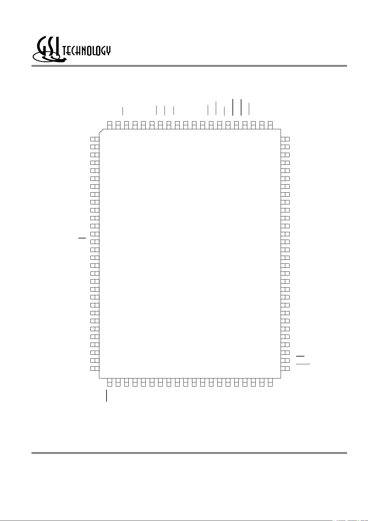
Pin Configuration
80
79
78
77
76
75
74
73
72
71
70
69
68
67
66
65
64
63
62
61
60
59
58
57
56
55
54
53
52
51
1
2
3
4
5
6
7
8
9
10
11
12
13
14
15
16
17
18
19
20
21
22
23
24
25
26
27
28
29
30
V
DDQ
V
SS
DQ9
DQ10
V
SS
V
DDQ
DQ11
DQ12
V
DD
NC
V
SS
DQ13
DQ14
V
DDQ
V
SS
DQ15
DQ16
DQP2
V
SS
V
DDQ
V
DDQ
V
SS
DQ8
DQ7
V
SS
VDDQ
DQ6
DQ5
V
SS
NC
V
DD
ZZ
DQ4
DQ3
V
DDQ
V
SS
DQ2
DQ1
V
SS
V
DDQ
LBO
A5
A4
A3
A2
A1
A0
TMS
TDI
V
SS
V
DD
TDO
TCK
A15
A14
A13
A12
A11
A17
A6
A7
CE1
CE2
NC
NC
BW2
BW1
CE3
CLK
GW
BWE
V
DD
V
SS
OE
ADSC
ADSP
ADVA8A9
A16
256K x 18
Top View
DQP1
A10
NC
NC
NC
NC
NC
DE
MATCH
MOE
NC
NC
NC
NC
NC
NC
NC
NC
NC
100 99 98 97 96 95 94 93 92 91 90 89 88 87 86 85 84 83 82 81
31 32 33 34 35 36 37 38 39 40 41 42 43 44 45 46 47 48 49 50
FT
Rev: 1.05 7/2001 3/30 © 1999, Giga Semiconductor, Inc.
Specifications cited are subject to change without notice. For latest documentation see http://www.gsitechnology.com.
GS84118T/B-166/150/130/100
84118 PadOut
119-Bump BGA—Top View
1 2 3 4 5 6 7
A
V
DDQ
A6 A7 ADSP A8 A9 V
DDQ
B
NC E2 A4 ADSC A15 E3 NC
C
NC A5 A3 V
DD
A14 A16 NC
D
DQB1 NC V
SS
NC V
SS
DQP1 NC
E
NC DQB2 V
SS
E1 V
SS
NC DQA8
F
V
DDQ
NC V
SS
G V
SS
DQA7 V
DDQ
G
NC DQB3 BB ADV NC NC DQA6
H
DQB4 NC V
SS
GW V
SS
DQA5 NC
J
V
DDQ
V
DD
NC V
DD
NC V
DD
V
DDQ
K
NC DQB5 V
SS
CK V
SS
NC DQA4
L
DQB6 NC NC NC BA DQA3 NC
M
V
DDQ
DQB7 V
SS
BW V
SS
MATCH V
DDQ
N
DQB8 NC V
SS
A1 V
SS
DQA2 DE
P
NC DQP2 V
SS
A0 V
SS
MOE DQA1
R
NC A2 LBO V
DD
FT A13 NC
T
NC A10 A11 NC A12 A17 ZZ
U
V
DDQ
TMS TDI NC TDO TCK V
DDQ
Rev: 1.05 7/2001 4/30 © 1999, Giga Semiconductor, Inc.
Specifications cited are subject to change without notice. For latest documentation see http://www.gsitechnology.com.
GS84118T/B-166/150/130/100
TQFP Pin Description
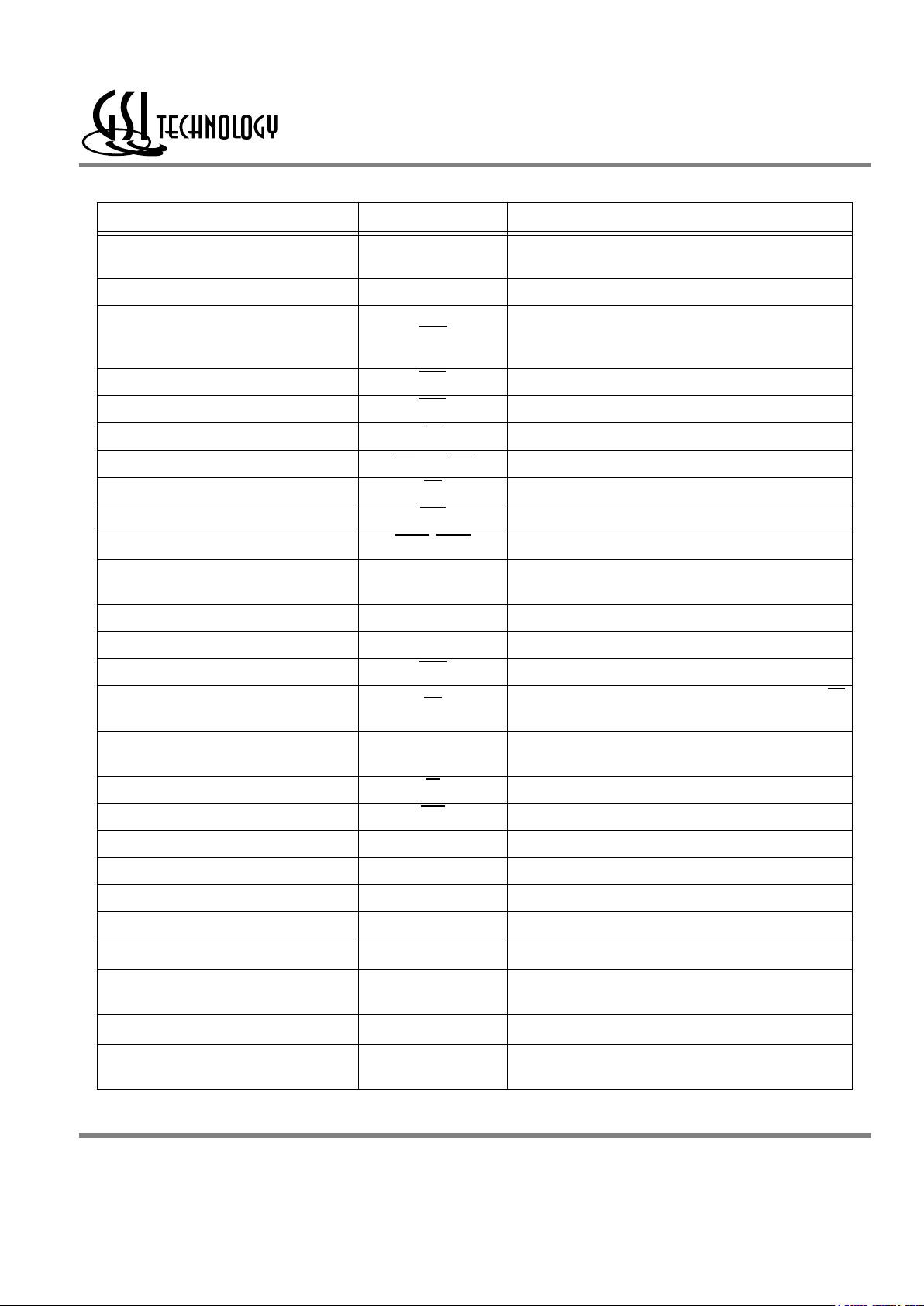
Pin Location Symbol Description
37, 36, 35, 34, 33, 32, 100, 99, 82, 81, 80, 48,
47, 46, 45, 44, 49, 50
A0–A17
Address Input Signals—Inputs are registered and must meet
setup and hold times, as specified on page 11.
89 CLK Clock Input Signal
87 BWE
Byte Write Enable Signal—The byte write enable signal
needs to be combined with one of the four byte write signals
for a write operation to occur.
93 BW1 Byte Write signal for data outputs 1 thru 8
94 BW2 Byte Write signal for data outputs 9 thru 16
88 GW Global Write Enable
92, 97, 98 CE1,CE2, CE3 Chip Enables
86 OE Output Enable
83 ADV Burst address advance
84, 85 ADSP, ADSC Address status signals
58, 59, 62 ,63, 68, 69, 72, 73, 8, 9, 12, 13, 18,
19, 22, 23
DQ1–DQ16 Data Input and Output pins
74, 24 DQP1–DQP2 Parity Input and Output pins
53 MATCH Match Output
51 MOE Match Output Enable
52 DE
Data Enable—Data input registers are updated only when DE
is active.
64 ZZ
Power down control—Application of ZZ will result in a low
standby power consumption.
14 FT Flow Through or Pipeline mode
31 LBO Linear Order Burst mode
38 TMS Test Mode Select
39 TDI Test Data In
42 TDO Test Data Out
43 TCK Test Clock
15, 41, 65, 91
V
DD
3.3 V power supply
5,10,17, 21, 26, 40, 55, 60, 67, 71,
76, 90
V
SS
Ground
4, 11, 20, 27, 54, 61, 70, 77
V
DDQ
2.5 V/3.3 V output power supply
1, 2, 3, 6, 7, 16, 25, 28, 29, 30,56, 57, 66, 75,
78, 79, 95, 96
NC No Connect
Rev: 1.05 7/2001 5/30 © 1999, Giga Semiconductor, Inc.
Specifications cited are subject to change without notice. For latest documentation see http://www.gsitechnology.com.
GS84118T/B-166/150/130/100
PBGA Pin Description
Pin Location Symbol Description
P4, N4, R2, C3, B3, C2, A2, A3, A5, A6, T6, C5,
R6, T5, T2, T3, B5, C6
A0–A17
Address Input Signals—Inputs are registered and must meet
setup and hold times, as specified on page 11.
K4 CLK Clock Input Signal
M4 BWE
Byte Write Enable Signal—The byte write enable signal needs to
be combined with one of the four byte write signals for a write
operation to occur.
L5 BW1 Byte Write signal for data outputs 1 thru 8
G3 BW2 Byte Write signal for data outputs 9 thru 16
H4 GW Global Write Enable
E4, B2, B6 CE1,CE2, CE3 Chip Enables
F4 OE Output Enable
G4 ADV Burst address advance
A4, B4 ADSP, ADSC Address status signals
P7, N6, L6, K7, H6, G7, F6, E7, D1, E2, G2, H1,
K2, L1, M2, N1
DQ1–DQ16 Data Input and Output pins
D6, P2 DQP1–DQP2 Parity Input and Output pins
M6 MATCH Match Output
P6 MOE Match Output Enable
N7 DE
Data Enable—Data input registers are updated only when DE is
active.
T7 ZZ
Power down control—Application of ZZ will result in a low
standby power consumption.
R5 FT Flow Through or Pipeline mode
R3 LBO Linear Order Burst mode
U2 TMS Test Mode Select
U3 TDI Test Data In
U5 TDO Test Data Out
U4 TCK Test Clock
C4, J2, J4, J6, R4
V
DD
3.3 V power supply
D3, D5, E3, E5, F3, F5, H3, H5, K3, K5, M3, M5,
N3, N5, P3, P5
V
SS
Ground
A1, A7, F1, F7, J1, J7, M1, M7, U1, U7
V
DDQ
2.5 V/3.3 V output power supply
B1, B7, C1, C7, D2, D4, D7, E1, E6, F2, G1, G5,
G6, H2, H7, J3, J5, K1, K6, L2, L3, L4, L7, N2,
P1, RR1, R7, T1, T4, U6
NC No Connect
Rev: 1.05 7/2001 6/30 © 1999, Giga Semiconductor, Inc.
Specifications cited are subject to change without notice. For latest documentation see http://www.gsitechnology.com.
GS84118T/B-166/150/130/100
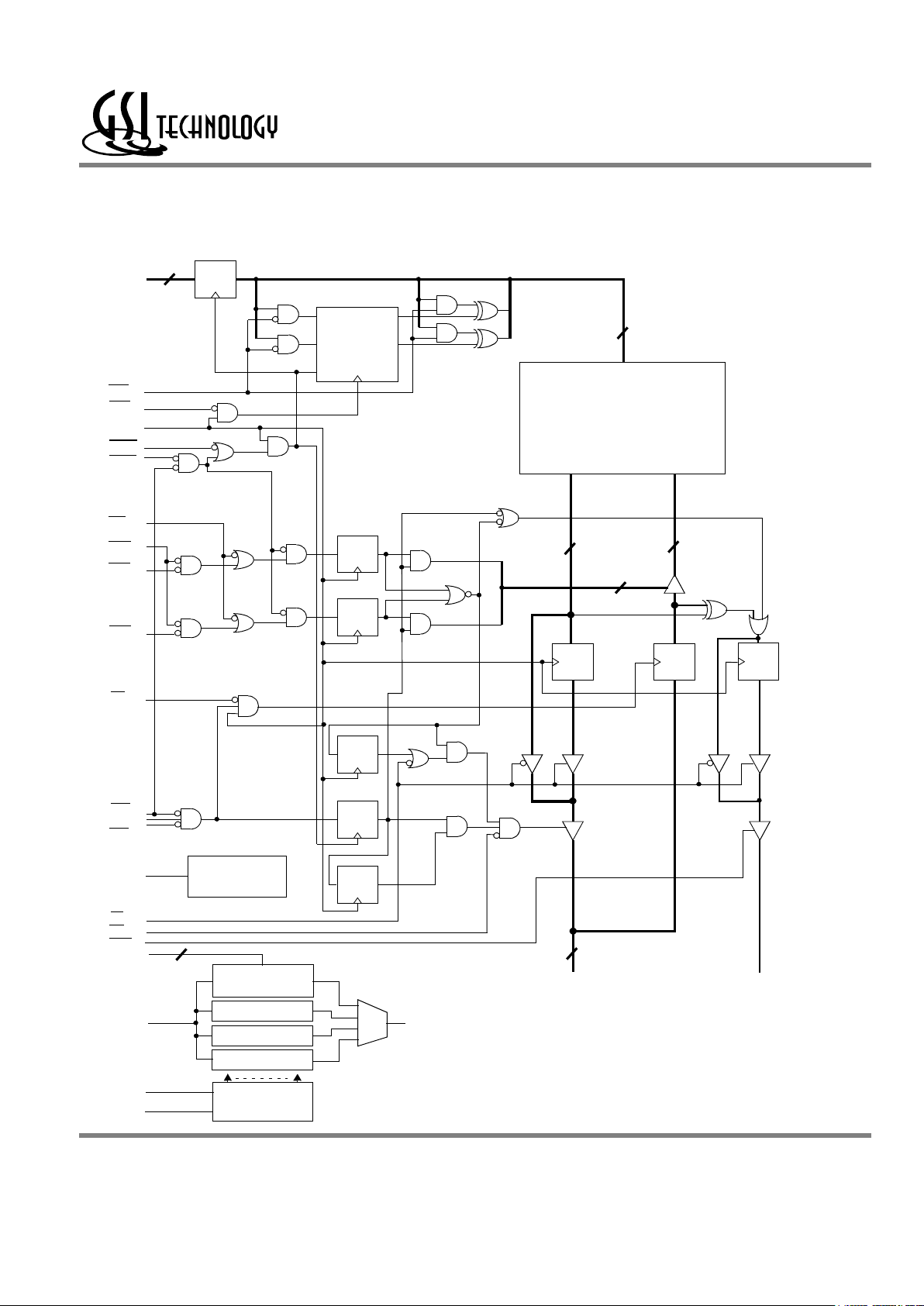
Functional Block Diagram
A1
A0
A0
A1
D0
D1
Q1
Q0
BINARY
COUNTER
Load
D Q
REGISTER
D Q
Register
D Q
Register
D Q
Register
D Q
Register
D Q
Register
D Q
Register
DQ
Register
A0-17
LBO
ADV
CLK
ADSC
ADSP
GW
BWE
BW1
BW2
CE1
CE2
CE3
FT
DQ1-16
OE
ZZ
Powerdown
Control
256K X 18
Memory
Array
18
18
18
18
2
18
A
Q D
DQP1-2
DE
D Q
Register
Match
TAP
Controller
Instruction Reg.
ID Reg.
Bypass Reg
Boundary Scan
Registers
54
TCK
TMS
TDI
A, DQ,
Control
TDO
MOE
Rev: 1.05 7/2001 7/30 © 1999, Giga Semiconductor, Inc.
Specifications cited are subject to change without notice. For latest documentation see http://www.gsitechnology.com.
GS84118T/B-166/150/130/100
Mode Pin Function
LBO Function
L Linear Burst
H or NC Interleaved Burst
FT Function
L Flow Through
H or NC Pipeline
Power Down Control
Note:
There are pull up devices on LBO and FT pins and pull down device on ZZ pin, so those input pins can be unconnected
and the chip will operate in the default states as specified in the above tables.
ZZ Function
L or NC Active
H Standby, IDD = ISB
Linear Burst Sequence
A[1:0] A[1:0] A[1:0] A[1:0]
1st address 00 01 10 11
2nd address 01 10 11 00
3rd address 10 11 00 01
4th address 11 00 01 10
Interleaved Burst Sequence
A[1:0] A[1:0] A[1:0] A[1:0]
1st address 00 01 10 11
2nd address 01 00 11 10
3rd address 10 11 00 01
4th address 11 10 01 00
Byte Write Function
Note: H = logic high, L = logic low, NC = no connect
Function GW BWE BW1 BW2
Read H H X X
Read H L H H
Write all bytes L X X X
Write all bytes H L L L
Write byte 1 H L L H
Write byte 2 H L H L
Rev: 1.05 7/2001 8/30 © 1999, Giga Semiconductor, Inc.
Specifications cited are subject to change without notice. For latest documentation see http://www.gsitechnology.com.
GS84118T/B-166/150/130/100
Synchronous Truth Table
Notes:
1. X means “don’t care,” H means “logic high,” L means “logic low.”
2. Write is the logic function of GW, BWE, BW1, BW2. See Byte Write Function table for detail.
3. All inputs, except OE, must meet setup and hold on rising edge of CLK.
4. Suspending busrt generates a wait cycle.
5. ADSP LOW along with SRAM being selected always initiates a Read cycle at the L-H edge of the clock (CLK).
6. A Write cycle can only be performed by setting Write low for the clock L-H edge of the subsequent wait cycle.
Refer to page 12 for the Write timing diagram.
Operation Address Used CE1 CE2 CE3 ADSP ADSC ADV Write OE CLK DQ
Deselect Cycle, Power Down none H X X X L X X X L-H High-Z
Deselect Cycle, Power Down none L L X L X X X X L-H High-Z
Deselect Cycle, Power Down none L X H L X X X X L-H High-Z
Deselect Cycle, Power Down none L L X H L X X X L-H High-Z
Deselect Cycle, Power Down none L X H H L X X X L-H High-Z
Read Cycle, Begin Burst external L H L L X X X L L-H Q
Read Cycle, Begin Burst external L H L L X X X H L-H High-Z
Read Cycle, Begin Burst external L H L H L X H L L-H Q
Read Cycle, Begin Burst external L H L H L X H H L-H High-Z
Write Cycle, Begin Burst external L H L H L X L X L-H D
Read Cycle, Continue Burst next X X X H H L H L L-H Q
Read Cycle, Continue Burst next X X X H H L H H L-H High-Z
Read Cycle, Continue Burst next H X X X H L H L L-H Q
Read Cycle, Continue Burst next H X X X H L H H L-H High-Z
Write Cycle, Continue Burst next X X X H H L L X L-H D
Write Cycle, Continue Burst next H X X X H L L X L-H D
Read Cycle, Suspend Burst current X X X H H H H L L-H Q
Read Cycle, Suspend Burst current X X X H H H H H L-H High-Z
Read Cycle, Suspend Burst current H X X X H H H L L-H Q
Read Cycle, Suspend Burst current H X X X H H H H L-H High-Z
Write Cycle, Suspend Burst current X X X H H H L X L-H D
Write Cycle, Suspend Burst current H X X X H H L X L-H D
Rev: 1.05 7/2001 9/30 © 1999, Giga Semiconductor, Inc.
Specifications cited are subject to change without notice. For latest documentation see http://www.gsitechnology.com.
GS84118T/B-166/150/130/100
Truth Table For Read/Write/Compare/Fill Write Operation
Notes:
1. X means “don’t care,” H means “logic high,” L means “logic low.”
2. Write is the logic function of GW, BWE, BW1, BW2. See Byte Write Function table for detail.
3. CE is defined as CE1=L, CE2=H and CE3=L
4. All signals are synchronous and are sampled by CLK except OE and MOE. OE and MOE are asynchronous and drive the bus immediately.
Absolute Maximum Ratings (Voltage reference to V
SS
= 0 V)
Note: Permanent damage to the device may occur if the Absolute Maximun Ratings are exceeded. Functional operation should be restricted to
the recommended operation conditions. Exposure to higher than recommended voltages, for an extended period of time, could effect the
performance and reliability of this component.
CE Write DE MOE OE Match DQ
Read L H X X L — Q
Write L L L X H — D
Compare L H L L H Data Out D
Fill Write L L H X X — X
Match Deselect H X X L X High High Z
Deselect H X X H X High Z High Z
Symbol Description Commerical Unit
V
DD
Supply Voltage –0.5 to 4.6 V
V
DDQ
Output Supply Voltage
–0.5 to V
DD
V
V
CLK
CLK Input Voltage –0.5 to 6 V
V
in
Input Voltage
–0.5 to VDD + 0.5
(≤ 4.6 V max. )
V
V
out
Output Voltage
–0.5 to VDD + 0.5
(≤ 4.6 V max. )
V
I
out
Output Current per I/O +/–20 mA
P
D
Power Dissipation 1.5 W
T
OPR
Operating Temperature 0 to 70
o
C
T
STG
Storage Temperature –55 to 125
o
C

Rev: 1.05 7/2001 10/30 © 1999, Giga Semiconductor, Inc.
Specifications cited are subject to change without notice. For latest documentation see http://www.gsitechnology.com.
GS84118T/B-166/150/130/100
Package Thermal Characteristics
Notes:
1. Junction temperature is a function of SRAM power dissapation, package thermal resistance, mounting board temperature, ambient.
Temperature air flow, board density, and PCB thermal resistance.
2. SCMI G-38-87.
3. Average thermal resistance between die and top surface, MIL SPEC-883, Method 1012.1.
Rating Layer Board Symbol TQFP max PBGA max Unit Notes
Junction to Ambient (at 200 lfm) single
R
ΘJA
32 28 °C/W 1,2
Junction to Ambient (at 200 lfm) four
R
ΘJA
20 18 °C/W 1,2
Junction to Case (TOP) —
R
ΘJC
7 4 °C/W 3
AC Test Conditions
(V
DD
= 3.135 V–3.6 V, TA = 0–70°C)
Notes:
1. Include scope and jig capacitance.
2. Test conditions as specified with output loading as shown in Fig. 1
unless otherwise noted.
3. Output load 2 for tLZ, tHZ, t
OLZ
and t
OHZ
.
4. Device is deselected as defined by the Truth Table.
Parameter Conditions
Input high level
VIH = 2.3 V
Input low level
VIL = 0.2 V
Input slew rate TR = 1 V/ns
Input reference level 1.25 V
Output reference level 1.25 V
Output load Fig. 1& 2
DQ
VT = 1.25 V
50W
30pF
1
DQ
2.5 V
FIG. 1
Output load 1
Output load 2
FIG. 2
225W
225W
5pF
1

Rev: 1.05 7/2001 11/30 © 1999, Giga Semiconductor, Inc.
Specifications cited are subject to change without notice. For latest documentation see http://www.gsitechnology.com.
GS84118T/B-166/150/130/100
DC Characteristics and Supply Currents (Voltage reference to V
SS
= 0 V)
(V
DD
= 3.135 V–3.6 V, Ta = 0–70°C for Commercial Temperature Offering)
Parameter Symbol Test Conditions Min Max
Input Leakage Current
(except ZZ, FT, LBO pins)
I
IL
V
IN
= 0 to V
DD
–1 uA 1 uA
ZZ Input Current
Iin
ZZ
V
DD ≥ VIN ≥ VIH
0 V ≤ V
IN
≤ V
IH
–1 uA
–1 uA
1 uA
300 uA
Mode Input Current
(FT & LBO pins)
Iin
M
V
DD ≥ VIN ≥ VIL
0 V ≤ V
IN
≤ V
IL
–30 0uA
–1 uA
1 uA
1 uA
Output Leakage Current
I
ol
Output Disable,
V
OUT
= 0 to V
DD
–1 uA 1 uA
Output High Voltage
V
OH
I
OH
= –4 mA, V
DDQ
= 2.375 V
1.7 V
Output High Voltage
V
OH
I
OH
= –4 mA, V
DDQ
= 3.135 V
2.4 V
Output Low Voltage
V
OL
I
OL
= +4 mA
0.4 V

Rev: 1.05 7/2001 12/30 © 1999, Giga Semiconductor, Inc.
Specifications cited are subject to change without notice. For latest documentation see http://www.gsitechnology.com.
GS84118T/B-166/150/130/100
Operating Currents
Parameter Test Conditions Symbol
-166 -150 -133 -100
Unit
0
to
70°°C
–40
to
+85°°C
0
to
70°°C
–40
to
+85°°C
0
to
70°°C
–40
to
+85°°C
0
to
70°°C
–40
to
+85°°C
Operating
Current
Device Selected;
All other inputs
≥ VIH Or ≤ V
IL
Output open
I
DD
Pipeline
310 320 275 285 250 260 190 200 mA
I
DD
Flow Through
190 200 190 200 140 150 140 150 mA
Standby Current
ZZ ≥ V
DD
– 0.2 V
I
SB
Pipeline
30 40 30 40 30 40 30 40 mA
I
SB
Flow Through
30 40 30 40 30 40 30 40 mA
Deselect Supply
Current
Device Deselected;
All other inputs
≥ VIH OR ≤ V
IL
I
DD
Pipeline
110 120 105 115 100 110 80 90 mA
I
DD
Flow Through
80 90 80 90 65 75 65 75 mA

Rev: 1.05 7/2001 13/30 © 1999, Giga Semiconductor, Inc.
Specifications cited are subject to change without notice. For latest documentation see http://www.gsitechnology.com.
GS84118T/B-166/150/130/100
AC Electrical Characteristics
Parameter Symbol
-166 -150 -133 -100
Unit
Min Max Min Max Min Max Min Max
Pipeline
Clock Cycle Time tKC 6.0 — 6.7 — 7.5 — 10 — ns
Clock to Output Valid tKQ — 3.5 — 3.8 — 4 — 4.5 ns
Clock to Output Invalid tKQX 1.5 — 1.5 — 1.5 — 1.5 — ns
Clock to Output in Low-Z
tLZ
1
1.5 — 1.5 — 1.5 — 1.5 — ns
Clock to Match Valid tKM — 3.5 — 3.8 — 4 — 4.5 ns
Clock to Match Invalid tKMX 1.5 — 1.5 — 1.5 — 1.5 — ns
Clock to Match in Low-Z
tMLZ
1
1.5 — 1.5 — 1.5 — 1.5 — ns
Flow-Thru
Clock Cycle Time tKC 10.0 — 10.0 — 15.0 — 15.0 — ns
Clock to Output Valid tKQ — 8.5 — 10.0 — 11.0 — 12.0 ns
Clock to Output Invalid tKQX 3.0 — 3.0 — 3.0 — 3.0 — ns
Clock to Output in Low-Z
tLZ
1
3.0 — 3.0 — 3.0 — 3.0 — ns
Clock to Match Valid tKM — 8.5 — 10.0 — 11.0 — 12.0 ns
Clock to Match Invalid tKMX 3.0 — 3.0 — 3.0 — 3.0 — ns
Clock to Match in Low-Z
tMLZ
1
3.0 — 3.0 — 3.0 — 3.0 — ns
Clock HIGH Time tKH 1.3 — 1.5 — 1.7 — 2 — ns
Clock LOW Time tKL 1.5 — 1.7 — 1.9 — 2.2 — ns
Clock to Output in High-Z
tHZ
1
1.5 3.5 1.5 3.8 1.5 4 1.5 5 ns
OE to Output Valid tOE — 3.5 — 3.8 — 4 — 5 ns
OE to output in Low-Z
tOLZ
1
0 — 0 — 0 — 0 — ns
OE to output in High-Z
tOHZ
1
— 3.5 — 3.8 — 4 — 5 ns
MOE to Match Valid tMOE — 3.5 — 3.8 — 4 — 5 ns
MOE to Match in Low-Z
tMOLZ
1
0 — 0 — 0 — 0 — ns
MOE to Match in High-Z
tMOHZ
1
— 3.5 — 3.8 — 4 — 5 ns

Rev: 1.05 7/2001 14/30 © 1999, Giga Semiconductor, Inc.
Specifications cited are subject to change without notice. For latest documentation see http://www.gsitechnology.com.
GS84118T/B-166/150/130/100
Notes:
1. These parameters are sampled and are not 100% tested
2. ZZ is an asynchronous signal. However, in order to be recognized on any given clock cycle, ZZ must meet the specified setup and hold
times as specified above.
Setup time tS 1.5 — 1.5 — 2.0 — 2.0 — ns
Hold time tH 0.5 — 0.5 — 0.5 — 0.5 — ns
ZZ setup time
tZZS
2
5 — 5 — 5 — 5 — ns
ZZ hold time
tZZH
2
1 — 1 — 1 — 1 — ns
ZZ recovery tZZR 20 — 20 — 20 — 20 — ns
AC Electrical Characteristics
Parameter Symbol
-166 -150 -133 -100
Unit
Min Max Min Max Min Max Min Max

Rev: 1.05 7/2001 15/30 © 1999, Giga Semiconductor, Inc.
Specifications cited are subject to change without notice. For latest documentation see http://www.gsitechnology.com.
GS84118T/B-166/150/130/100
CLK
ADSP
ADSC
ADV
GW
CE1
BWE
CE3
OE
WR2 WR3
WR1
WR1
WR2 WR3
t
KC
Single Write
Burst Write
D2a D2b
D2c D2d D3a
D1a
t
KL
t
KH
t
S
t
H
t
S
t
H
t
S
t
H
t
S
t
H
tSt
H
t
S
t
H
t
S
t
H
t
S
t
H
t
S
t
H
t
S
t
H
t
S
t
H
Write specified byte for 2a and all bytes for 2b, 2c& 2d
CE2 and CE3 only sampled with ADSP or ADSC
CE1 masks ADSP
ADV must be inactive for ADSP Write
ADSC initiated write
ADSP is blocked by CE1 inactive
Write Cycle Timing
A0–A17
BW1–
BW2
CE2
DQ1–16
Write
Deselected
Hi-Z
WR1 WR2 WR3
Deselected with CE2
DQP1–2
DE
t
S
t
H

Rev: 1.05 7/2001 16/30 © 1999, Giga Semiconductor, Inc.
Specifications cited are subject to change without notice. For latest documentation see http://www.gsitechnology.com.
GS84118T/B-166/150/130/100
Q1a
Q3a
Q2d
Q2cQ2b
Q2a
t
KQ
t
LZ
t
OE
t
OHZ
t
OLZ
t
KQX
t
HZ
t
KQX
CLK
ADSP
ADSC
BWE
OE
GW
ADV
CE2
Single Read
RD2 RD3
t
KL
t
S
t
H
t
H
t
H
t
S
t
H
t
H
t
S
t
H
t
S
t
H
ADSC initiated read
Suspend Burst
CE1 masks ADSP
CE2 and CE3 only sampled with ADSP or ADSC
Deselected with CE2
Single Read
ADSP is blocked by CE1 inactive
A0–A17
BW1–
CE3
CE1
t
KH
t
KC
t
S
t
H
t
S
t
S
t
H
BW2
DQ1–16
t
S
t
S
RD1
Hi-Z
Suspend Burst
DQP1–2
Flow Through—Read Cycle Timing

Rev: 1.05 7/2001 17/30 © 1999, Giga Semiconductor, Inc.
Specifications cited are subject to change without notice. For latest documentation see http://www.gsitechnology.com.
GS84118T/B-166/150/130/100
CLK
ADSP
ADSC
ADV
GW
BWE
CE1
CE3
OE
CE2
RD1
WR1
RD2
WR1
Q1a D1a
Q2a
Q2b Q2c
Q2d
Single Read
Burst Read
t
OE
t
OHZ
t
S
t
S
t
H
t
S
tSt
H
t
S
t
H
t
H
tSt
H
t
S
t
H
t
S
t
H
t
S
t
H
t
KH
ADSC initiated read
CE1 masks ADSP
CE2 and CE3 only sampled with ADSP and ADSC
Deselected with CE3
DQ1–16
BW1–
BW2
A0–A17
t
KL
t
KC
t
S
t
H
t
H
Single Write
ADSP is blocked by CE1 inactive
t
KQ
t
S
t
H
Hi-Z
Q2a
Burst wrap around to its initial state
DQP1–2
Flow Through—Read/Write Cycle Timing
t
S
t
H
DE
Rev: 1.05 7/2001 18/30 © 1999, Giga Semiconductor, Inc.
Specifications cited are subject to change without notice. For latest documentation see http://www.gsitechnology.com.
GS84118T/B-166/150/130/100
Q1a
Q3a
Q2d
Q2c
Q2b
Q2a
t
KQ
t
LZ
t
OE
t
OHZ
t
OLZ
t
KQX
t
HZ
t
KQX
CLK
ADSP
ADSC
BWE
OE
GW
ADV
CE2
Burst Read
RD2
RD3
t
KL
t
S
t
H
t
H
t
H
t
S
t
H
t
H
t
S
t
H
t
S
t
H
ADSC initiated read
Suspend Burst
CE1 masks ADSP
CE2 and CE3 only sampled with ADSP or ADSC
Deselected with CE2
Single Read
ADSP is blocked by CE1 inactive
A0–A17
BW1–
CE3
CE1
t
KH
t
KC
t
S
t
H
t
S
t
S
t
H
BW4
DQ1–16
t
S
t
S
RD1
Hi-Z
DQP1–2
Pipeline—Read Cycle Timing

Rev: 1.05 7/2001 19/30 © 1999, Giga Semiconductor, Inc.
Specifications cited are subject to change without notice. For latest documentation see http://www.gsitechnology.com.
GS84118T/B-166/150/130/100
t
S
t
H
DE
CLK
ADSP
ADSC
ADV
GW
BWE
CE1
CE3
OE
CE2
RD1
WR1
RD2
WR1
Q1a
D1a
Q2a
Q2b Q2c
Q2d
Single Read Burst Read
t
OE
t
OHZ
t
S
t
S
t
H
t
S
t
S
t
H
t
S
t
H
t
H
t
S
t
H
t
S
t
H
t
S
t
H
t
S
t
H
t
KH
ADSC initiated read
CE1 masks ADSP
CE2 and CE3 only sampled with ADSP and ADSC
Deselected with CE3
DQ1–16
BW1–
BW4
A0–A17
t
KL
t
KC
t
S
t
H
t
H
Single Write
ADSP is blocked by CE1 inactive
t
KQ
t
S
t
H
Hi-Z
DQP1–2
Pipeline—Read/Write Cycle Timing

Rev: 1.05 7/2001 20/30 © 1999, Giga Semiconductor, Inc.
Specifications cited are subject to change without notice. For latest documentation see http://www.gsitechnology.com.
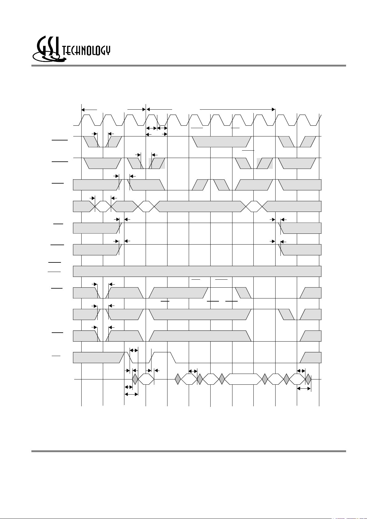
GS84118T/B-166/150/130/100
Hit
Miss
Fill Write
CLK
CE
(1)
W
(2)
OE
A0-A17
DQ1-16
DQP1-2
DE
MOE
MATCH
t
S
t
H
A
B B
A B
t
MLZ
t
MOE
t
KM
t
KMX
Match high when chip deselected
Flow Through—Compare/Fill Write Cycle Timing
t
KM
t
KM
2. W = L is the Asertive function of GW, BWE, BW1, BW2. See Byte Write Function table for detail.
1. CE = L is defined as CE1=L, CE2=H and CE3=L
Notes:

Rev: 1.05 7/2001 21/30 © 1999, Giga Semiconductor, Inc.
Specifications cited are subject to change without notice. For latest documentation see http://www.gsitechnology.com.
GS84118T/B-166/150/130/100
Hit Miss Fill Write
CLK
CE
(1)
W
(2)
OE
A0-A17
DQ1-16
DQP1-2
DE
MOE
MATCH
t
S
t
H
A
B B
A B
t
MLZ
t
MOE
t
KM
t
KMX
Match high when chip deselected
Pipeline—Compare/Fill Write Cycle Timing
2. W = L is the Asertive function of GW, BWE, BW1, BW2. See Byte Write Function table for detail.
1. CE = L is defined as CE1=L, CE2=H and CE3=L
Notes:
t
KM
t
KM

Rev: 1.05 7/2001 22/30 © 1999, Giga Semiconductor, Inc.
Specifications cited are subject to change without notice. For latest documentation see http://www.gsitechnology.com.
GS84118T/B-166/150/130/100
CLK
ADSP
ADSC
t
H
t
KH
t
KL
t
KC
t
S
ZZ
t
ZZR
t
ZZH
t
ZZS
~
~
~
~
~
~
~
~
~
~
~
~
~
~
Snooze
ZZ Timing

Rev: 1.05 7/2001 23/30 © 1999, Giga Semiconductor, Inc.
Specifications cited are subject to change without notice. For latest documentation see http://www.gsitechnology.com.
GS84118T/B-166/150/130/100
Test Mode Description
Functional Description
The GS84118 provides JTAG boundary scan interface using IEEE standard 1149.1 protocol. The Test mode is intended to provide
a mechanism for testing the interconnect between master (processor, controller, etc.), SRAM, other components and the Printed
Circuit Board.
Test Access Port (TAP)
Four pins (as defined in Pin Description Tables) are used to performed JTAG functions. TDI input is used to scan test data serially
into one of three registers (Instruction Register, Boundary Scan Register and Bypass Register). TDO is the output pin to serially
output scan test data. The TDI sends the data into the LSB of the selected register and the MSB of that register feeds the data to
TDO. TMS input pin controls the state transition of 16 state TAP controllers, as specified in IEEE standard 1149.1. Inputs on TDI
and TMS are registered on the rising edge of TCK clock, and the output data on TDO is presented on the falling edge of TCK. The
TDO driver is in active state only when TAP controller is in Shift-IR state or in Shift -DR state.
TAP Controller
Sixteen state controllers are implemented as specified in IEEE standard 1149.1.
The controller enters the Reset state either through
• Power up or
• Apply logic 1 on TMS input pin on 5 consecutive rising edges.
Select DR
Capture DR
Shift DR
Exit1 DR
Pause DR
Exit2 DR
Update DR
Select IR
Capture IR
Shift IR
Exit1 IR
Pause IR
Exit2 IR
Update IR
Test Logic Reset
Run Test Idle
0
0
1
0
1
1
0
0
1
1
1
0
0
1
1
0
0
0
0
1
1
0 0
1
1 0
0
0
1
1 1 1
Tap Controller State Diagram

Rev: 1.05 7/2001 24/30 © 1999, Giga Semiconductor, Inc.
Specifications cited are subject to change without notice. For latest documentation see http://www.gsitechnology.com.
GS84118T/B-166/150/130/100
Instruction Register (3 Bits)
The JTAG Instruction register is consisted of shift register stage and parallel output latch. The register is 3 bits wide and is encoded
as follow:
Bypass Register (1 Bit)
The Bypass Register is one bit wide and is connected electrically between TDI and TDO and provides the minimum length serially
path between TDI and TDO.
ID Register (32 Bits)
The ID Register are 32 bits wide and are listed as follow:
Octal MSB — LSB Instruction
0 0 0 0 Bypass
1 0 0 1 IDCODE—Read device ID
2 0 1 0 Sample-Z—Sample Inputs and tri-state DQs, Match
3 0 1 1 Bypass
4 1 0 0 Sample—Sample Inputs
5 1 0 1 Private—Manufacturer use only
6 1 1 0 Bypass
7 1 1 1 Bypass
Header ID[0] 1
GSI ID
(89 decimal in bank 2)
ID[7:1] 101 1001
ID[11:8] 0001
Part Number ID[27:12] 0000 0000 0000 0000
Revision Number ID[31:28] xxxx

Rev: 1.05 7/2001 25/30 © 1999, Giga Semiconductor, Inc.
Specifications cited are subject to change without notice. For latest documentation see http://www.gsitechnology.com.
GS84118T/B-166/150/130/100
Boundary Scan Register (54 Bits)
The Boundary Scan Register are 54 bits wide and are listed as follow:
Scan Order (Order by exit sequence)
DQx, Match 19
Address 18
GW, BWE, BW1-2, DE 5
CE1, CE2, CE3 3
OE, MOE 2
ADSP, ADSC, ADV 3
ZZ, FT, LBO 3
CLK 1
Total 54
Order Signal TQFP BGA Order Signal TQFP BGA
1
2
3
4
5
6
7
8
9
10
11
12
13
14
15
16
17
18
19
20
21
22
23
24
25
26
27
A15
A14
A13
A12
A11
A16
A17
MOE
DE
MATCH
DQ1
DQ2
DQ3
DQ4
ZZ
DQ5
DQ6
DQ7
DQ8
DQP1
A10
A9
A8
ADV
ADSP
ADSC
OE
44
45
46
47
48
49
50
51
52
53
58
59
62
63
64
68
69
72
73
74
80
81
82
83
84
85
86
3T
2T
5T
6R
5C
5B
6C
6P
7N
6M
7P
6N
6L
7K
7T
6H
7G
6F
7E
6D
6T
6A
5A
4G
4A
4B
4F
28
29
30
31
32
33
34
35
36
37
38
39
40
41
42
43
44
45
46
47
48
49
50
51
52
53
54
BWE
GW
CLK
CE3
BW1
BW2
CE2
CE1
A7
A6
DQ9
DQ10
DQ11
DQ12
FT
DQ13
DQ14
DQ15
DQ16
DQP2
LBO
A5
A4
A3
A2
A1
A0
87
88
89
92
93
94
97
98
99
100
8
9
12
13
14
18
19
22
23
24
31
32
33
34
35
36
37
4M
4H
4K
6B
5L
3G
2B
4E
3A
2A
1D
2E
2G
1H
5R
2K
1L
2M
1N
2P
3R
2C
3B
3C
2R
4N
4P

Rev: 1.05 7/2001 26/30 © 1999, Giga Semiconductor, Inc.
Specifications cited are subject to change without notice. For latest documentation see http://www.gsitechnology.com.
GS84118T/B-166/150/130/100
Test Mode AC Electrical Characteristics
Test Mode Timing Diagram
Parameter Symbol Min Max Unit
TCK Cycle Time tTKC 20 — ns
TCK Low to TDO Valid tTKQ — 10 ns
TCK High Pulse Width tTKH 10 — ns
TCK Low Pulse Width tTKL 10 — ns
TDI & TMS Set Up Time tTS 5 — ns
TDI & TMS Hold Time tTH 5 — ns
t
TKC
t
TKQ
t
TS
t
TH
t
TKH
t
TKL
TCK
TMS
TDI
TDO

Rev: 1.05 7/2001 27/30 © 1999, Giga Semiconductor, Inc.
Specifications cited are subject to change without notice. For latest documentation see http://www.gsitechnology.com.
GS84118T/B-166/150/130/100
Package Dimensions—100-Pin TQFP
D1
D
E1
E
Pin 1
b
e
c
L
L1
A2
A1
Y
θ
Symbol Description Min. Nom. Max
A1 Standoff 0.05 0.10 0.15
A2 Body Thickness 1.35 1.40 1.45
B Lead Width 0.20 0.30 0.40
C Lead Thickness 0.09 0.20
D Terminal Dimension 21.9 22.0 22.1
D1 Package Body 19.9 20.0 20.1
E Terminal Dimension 15.9 16.0 16.1
E1 Package Body 13.9 14.0 14.1
E Lead Pitch 0.65
L Foot Length 0.45 0.60 0.75
L1 Lead Length 1.00
Y Coplanarity 0.10
Q Lead Angle 0° 7°
Notes:
1. All dimesnions are in millimeters (mm).
2. Package wideth and length do not include mold protrusion.

Rev: 1.05 7/2001 28/30 © 1999, Giga Semiconductor, Inc.
Specifications cited are subject to change without notice. For latest documentation see http://www.gsitechnology.com.
GS84118T/B-166/150/130/100
Package Dimesions - 119 Pin PBGA
BPR 1999.05.18
N
P
A
B
Pin 1
Corner
K
E
F
C T
A
B
C
D
E
F
G
H
J
K
L
M
N
P
R
T
U
G
S
D
1234567
Package Dimesions - 119 Pin PBGA
Unit: mm
Symbo
l
Description
Min.Nom.Ma
x
A Width 13.8 14.0 14.2
B Length 21.8 22.0 22.2
C Package Height (including ball) - 2.40
D Ball Size 0.60 0.75 0.90
E Ball Height 0.50 0.60 0.70
F Package Height (excluding balls) 1.46 1.70
G Width between Balls 1.27
K Package Height above board 0.80 0.90 1.00
N Cut-out Package Width 12.00
P Foot Length 19.50
R Width of package between balls 7.62
S Length of package between balls 20.32
T Variance of Ball Height 0.15
Bottom View
R
Top View
Side View

Rev: 1.05 7/2001 29/30 © 1999, Giga Semiconductor, Inc.
Specifications cited are subject to change without notice. For latest documentation see http://www.gsitechnology.com.
GS84118T/B-166/150/130/100
Ordering Information
Org
Part Number
1
Type Package
Speed
2
(MHz/ns)
T
A
3
Status
256K x 18 GS84118T-166 Pipeline/Flow Through TQFP 166/8.5 C
256K x 18 GS84118T-150 Pipeline/Flow Through TQFP 150/10 C
256K x 18 GS84118T-133 Pipeline/Flow Through TQFP 133/11 C
256K x 18 GS84118T-100 Pipeline/Flow Through TQFP 100/12 C
256K x 18 GS84118T-166I Pipeline/Flow Through TQFP 166/8.5 I
256K x 18 GS84118T-150I Pipeline/Flow Through TQFP 150/10 I
256K x 18 GS84118T-133I Pipeline/Flow Through TQFP 133/11 C
256K x 18 GS84118T-100I Pipeline/Flow Through TQFP 100/12 I
256K x 18 GS84118B-166 Pipeline/Flow Through BGA 166/8.5 C
256K x 18 GS84118B-150 Pipeline/Flow Through BGA 150/10 C
256K x 18 GS84118B-133 Pipeline/Flow Through BGA 133/11 C
256K x 18 GS84118B-100 Pipeline/Flow Through BGA 100/12 C
256K x 18 GS84118B-166I Pipeline/Flow Through BGA 166/8.5 I
256K x 18 GS84118B-150I Pipeline/Flow Through BGA 150/10 I
256K x 18 GS84118I-133I Pipeline/Flow Through BGA 133/11 C
256K x 18 GS84118B-100I Pipeline/Flow Through BGA 100/12 I
Notes:
1. Customers requiring delivery in Tape and Reel should add the character “T” to the end of the part number. Example: GS84032T-7.5T.
2. The speed column indicates the cycle frequency (Mhz) of the device in Pipelined mode and the latency (ns) in Flow Through mode. Each
device is Pipeline / Flow through mode selectable by the user.
3. TA = C = Commercial Temperature Range. TA = I = Industrial Temperature Range.
4. GSI offers other versions this type of device in many different configurations and with a variety of different features, only some of which
are covered in this data sheet. See the GSI Technology web site for a complete listing of current offerings.

Rev: 1.05 7/2001 30/30 © 1999, Giga Semiconductor, Inc.
Specifications cited are subject to change without notice. For latest documentation see http://www.gsitechnology.com.
GS84118T/B-166/150/130/100
4Mb Synchronous Tag RAM Datasheet Revision History
Rev. Code: Old;New
Types of Changes
Format or Content
Page /Revisions;Reason
GS84118-2000207; 84118_r1_01 Content
• Updated BGA Pin Description to meet JEDEC standard
84118_r1_02; 84118_r1_03 Content/Format
• Updated format to comply with Technical Publications
standards
• Corrected typo in TQFP Package Description table on page
27
84118_r1_03; 84118_r1_04 Content
• Updated Pinout on page 3
• Updated Pin Description tables for TQFP and PBGA
• Added overbar to all references of BWE, BW1, BW2, GW,
CE1, CE3, OE, ADV, ADSP, ADSC, MOE, DE, FT, and LBO
• Removed VDD note from AC Electrical Characteristics table
• Imported up-to-date Package Drawing for 119 PBGA
84118_r1_04; 84118_r1_05 Content
• Reordered pin location listings in pin description tables on
pages 4 and 5
• Removed Global Write reference from BWE description in pin
description tables
• Removed BWE reference from GW description in pin
description tables
• Placed overbars on Write references in Synchronous Truth
Table
 Loading...