

GSI GS8324Z72C-250I, GS8324Z72C-250, GS8324Z36C-150, GS8324Z36C-133, GS8324Z36B-250I Datasheet
...
Preliminary
GS8324Z18(B/C)/GS8324Z36(B/C)/GS8324Z72(C)
119- and 209-Pin BGA
2M x 18, 1M x 36, 512K x 72
Commercial Temp
Industrial Temp
36Mb Sync NBT SRAMs
Features
• NBT (No Bus Turn Around) functionality allows zero wait
Read-Write-Read bus utilization; fully pin-compatible with
both pipelined and flow through NtRAM™, NoBL™ and
ZBT™ SRAMs
• FT pin for user-configurable flow through or pipeline operation
• IEEE 1149.1 JTAG-compatible Boundary Scan
• ZQ mode pin for user-selectable high/low output drive
• 2.5 V or 3.3 V +10%/–5% core power supply
• 2.5 V or 3.3 V I/O supply
• LBO pin for Linear or Interleaved Burst mode
• Byte Write (BW) and/or Global Write (GW) operation
• Internal self-timed write cycle
• Automatic power-down for portable applications
• JEDEC-standard 119- and 209-bump BGA package
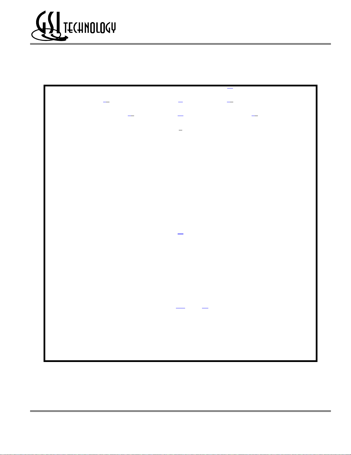
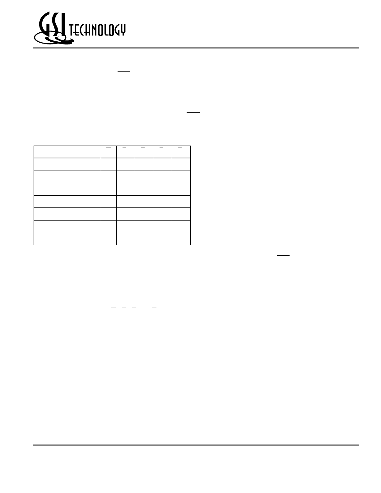
-250 -225 -200 -166 -150 -133 Unit
Pipeline
3-1-1-1
3.3 V
2.5 V
Flow
Through
2-1-1-1
3.3 V
2.5 V
t
KQ
tCycle
Curr (x18)
Curr (x36)
Curr (x72)
Curr (x18)
Curr (x36)
Curr (x72)
t
KQ
tCycle
Curr (x18)
Curr (x36)
Curr (x72)
Curr (x18)
Curr (x36)
Curr (x72)
2.3
4.0
365
560
660
360
550
640
6.0
7.0
235
300
350
235
300
340
2.5
4.4
335
510
600
330
500
590
6.5
7.5
230
300
350
230
300
340
3.0
3.5
5.0
6.0
305
265
460
400
540
460
305
260
460
390
530
450
7.5
8.51010101115ns
8.5
210
200
270
270
300
300
210
200
270
270
300
300
3.8
6.6
245
370
430
240
360
420
195
270
300
195
270
300
4.0
7.5nsns
215
mA
330
mA
380
mA
215
mA
330
mA
370
mA
150
mA
200
mA
220
mA
145
mA
190
mA
220
mA
250 MHz–133MHz
2.5 V or 3.3 V V
2.5 V or 3.3 V I/O
with either ADSP or ADSC inputs. In Burst mode, subsequent
burst addresses are generated internally and are controlled by
ADV. The burst address counter may be configured to count in
either linear or interleave order with the Linear Burst Order (LBO)
input. The Burst function need not be used. New addresses can be
loaded on every cycle with no degradation of chip performance.
Flow Through/Pipeline Reads
The function of the Data Output register can be controlled by the
user via the FT mode . Holding the FT mode pin low places the
RAM in Flow Through mode, causing output data to bypass the
Data Output Register. Holding FT high places the RAM in
Pipeline mode, activating the rising-edge-triggered Data Output
Register.
Byte Write and Global Write
Byte write operation is performed by using Byte Write enable
(BW) input combined with one or more individual byte write
signals (Bx). In addition, Global Write (GW) is available for
writing all bytes at one time, regardless of the Byte Write control
inputs.
FLXDrive™
The ZQ pin allows selection between high drive strength (ZQ low)
for multi-drop bus applications and normal drive strength (ZQ
floating or high) point-to-point applications. See the Output Driver
Characteristics chart for details.
Sleep Mode
Low power (Sleep mode) is attained through the assertion (High)
of the ZZ signal, or by stopping the clock (CK). Memory data is
ns
retained during Sleep mode.
Core and Interface Voltages
The GS8324Z18/36/72 operates on a 2.5 V or 3.3 V power supply.
All input are 3.3 V and 2.5 V compatible. Separate output power
(V
) pins are used to decouple output noise from the internal
DDQ
circuits and are 3.3 V and 2.5 V compatible.
DD
Functional Description
Applications
The GS8324Z18/36/72 is a 37,748,736-bit high performance 2-die
synchronous SRAM module with a 2-bit burst address counter.
Although of a type originally developed for Level 2 Cache
applications supporting high performance CPUs, the device now
finds application in synchronous SRAM applications, ranging
from DSP main store to networking chip set support.
Controls
Addresses, data I/Os, chip enable (E1), address burst control
inputs (ADSP, ADSC, ADV), and write control inputs (Bx, BW,
GW) are synchronous and are controlled by a positive-edgetriggered clock input (CK). Output enable (G) and power down
control (ZZ) are asynchronous inputs. Burst cycles can be initiated
Rev: 1.00 10/2001 1/46 © 2001, Giga Semiconductor, Inc.
Specifications cited are subject to change without notice. For latest documentation see http://www.gsitechnology.com.
NoBL is a trademark of Cypress Semiconductor Corp.. NtRAM is a trademark of Samsung Electronics Co.. ZBT is a trademark of Integrated Device Technology, Inc.

Preliminary
GS8324Z18(B/C)/GS8324Z36(B/C)/GS8324Z72(C)
GS8324Z72B Pad Out
209-Bump BGA—Top View
1 2 3 4 5 6 7 8 9 10 11
A DQG5 DQG1 A13 E2 A14 ADV A15 E3 A17 DQB1 DQB5 A
B DQG6 DQG2 BC BG NC W A16 BB BF DQB2 DQB6 B
C DQG7 DQG3 BH BD NC E1 NC BE BA DQB3 DQB7 C
V
V
V
V
DDQ
V
DDQ
V
DDQ
SS
SS
SS
NC NC G NC NC
V
DDQ
V
V
DDQ
V
V
DDQ
D DQG8 DQG4
E DQPG9 DQPC9
F DQC4 DQC8
G DQC3 DQC7
H DQC2 DQC6
J DQC1 DQC5
K NC NC CK NC
L DQH1 DQH5
M DQH2 DQH6
N DQH3 DQH7
P DQH4 DQH8
R DQPD9 DQPH9
V
V
V
DDQ
V
DDQ
V
DDQ
SS
SS
V
V
V
DDQ
V
DDQ
V
DDQ
SS
SS
SS
SS
V
SS
V
DD
V
SS
V
DD
V
SS
V
DD
V
SS
V
DD
V
SS
V
DD
V
SS
V
DD
V
DD
ZQ
MCH
MCL
MCH
MCL
FT
MCL
MCH
ZZ
V
DD
V
DD
V
SS
V
DD
V
SS
V
DD
V
SS
V
DD
V
SS
V
DD
V
SS
V
DD
V
V
V
DDQ
V
DDQ
V
DDQ
SS
SS
V
V
V
DDQ
V
DDQ
V
DDQ
SS
SS
NC NC NC NC K
V
V
V
DDQ
V
DDQ
V
DDQ
SS
SS
V
V
V
DDQ
V
DDQ
V
DDQ
SS
SS
DQB4 DQB8 D
DQPF9 DQPB9 E
DQF8 DQF4 F
DQF7 DQF3 G
DQF6 DQF2 H
DQF5 DQF1 J
DQA5 DQA1 L
DQA6 DQA2 M
DQA7 DQA3 N
DQA8 DQA4 P
DQPA9 DQPE9 R
T DQD8 DQD4
V
SS
NC NC LBO PE NC
V
SS
DQE4 DQE8 T
U DQD7 DQD3 NC A12 NC A11 A18 A10 NC DQE3 DQE7 U
V DQD6 DQD2 A9 A8 A7 A1 A6 A5 A4 DQE2 DQE6 V
W DQD5 DQD1 TMS TDI A3 A0 A2 TDO TCK DQE1 DQE5 W
11 x 19 Bump BGA—14 x 22 mm2 Body—1 mm Bump Pitch
Rev: 1.00 10/2001 2/46 © 2001, Giga Semiconductor, Inc.
Specifications cited are subject to change without notice. For latest documentation see http://www.gsitechnology.com.
Preliminary
GS8324Z18(B/C)/GS8324Z36(B/C)/GS8324Z72(C)
GS8324Z36C Pad Out
209-Bump BGA—Top View
1 2 3 4 5 6 7 8 9 10 11
A NC NC A13 E2 A14 ADV A15 E3 A17 DQB1 DQB5 A
B NC NC BC NC A19 W A16 BB NC DQB2 DQB6 B
C NC NC NC BD NC E1 NC NC BA DQB3 DQB7 C
V
V
V
V
DDQ
V
DDQ
V
DDQ
SS
SS
SS
NC NC G NC NC
V
DDQ
V
V
DDQ
V
V
DDQ
D NC NC
E NC DQPC9
F DQC4 DQC8
G DQC3 DQC7
H DQC2 DQC6
J DQC1 DQC5
K NC NC CK NC
L NC NC
M NC NC
N NC NC
P NC NC
R DQPD9 NC
V
V
V
DDQ
V
DDQ
V
DDQ
SS
SS
V
V
V
DDQ
V
DDQ
V
DDQ
SS
SS
SS
SS
V
SS
V
DD
V
SS
V
DD
V
SS
V
DD
V
SS
V
DD
V
SS
V
DD
V
SS
V
DD
V
DD
ZQ
MCH
MCL
MCH
MCL
FT
MCL
MCH
ZZ
V
DD
V
DD
V
SS
V
DD
V
SS
V
DD
V
SS
V
DD
V
SS
V
DD
V
SS
V
DD
V
V
V
DDQ
V
DDQ
V
DDQ
SS
SS
V
V
V
DDQ
V
DDQ
V
DDQ
SS
SS
NC NC NC NC K
V
V
V
DDQ
V
DDQ
V
DDQ
SS
SS
V
V
V
DDQ
V
DDQ
V
DDQ
SS
SS
DQB4 DQB8 D
NC DQPB9 E
NC NC F
NC NC G
NC NC H
NC NC J
DQA5 DQA1 L
DQA6 DQA2 M
DQA7 DQA3 N
DQA8 DQA4 P
DQPA9 NC R
T DQD8 DQD4
V
SS
NC NC LBO PE NC
V
SS
NC NC T
U DQD7 DQD3 NC A12 NC A11 A18 A10 NC NC NC U
V DQD6 DQD2 A9 A8 A7 A1 A6 A5 A4 NC NC V
W DQD5 DQD1 TMS TDI A3 A0 A2 TDO TCK NC NC W
11 x 19 Bump BGA—14 x 22 mm2 Body—1 mm Bump Pitch
Rev: 1.00 10/2001 3/46 © 2001, Giga Semiconductor, Inc.
Specifications cited are subject to change without notice. For latest documentation see http://www.gsitechnology.com.

Preliminary
GS8324Z18(B/C)/GS8324Z36(B/C)/GS8324Z72(C)
GS8324Z18C Pad Out
209-Bump BGA—Top View
1 2 3 4 5 6 7 8 9 10 11
A NC NC A13 VDD A14 ADV A15 VSS A17 NC NC A
B NC NC BB NC A19 W A16 NC NC NC NC B
C NC NC NC NC NC E1 A20 NC BA NC NC C
V
V
V
V
DDQ
V
DDQ
V
DDQ
SS
SS
SS
NC NC G NC NC
V
DDQ
V
V
DDQ
V
V
DDQ
D NC NC
E NC DQPB9
F DQB4 DQB8
G DQB3 DQB7
H DQB2 DQB6
J DQB1 DQB5
K NC NC CK NC
L NC NC
M NC NC
N NC NC
P NC NC
R NC NC
V
V
V
DDQ
V
DDQ
V
DDQ
SS
SS
V
V
V
DDQ
V
DDQ
V
DDQ
SS
SS
SS
SS
V
SS
V
DD
V
SS
V
DD
V
SS
V
DD
V
SS
V
DD
V
SS
V
DD
V
SS
V
DD
V
DD
ZQ
MCH
MCL
MCH
MCL
FT
MCL
VDD
ZZ
V
DD
V
DD
V
SS
V
DD
V
SS
V
DD
V
SS
V
DD
V
SS
V
DD
V
SS
V
DD
V
V
V
DDQ
V
DDQ
V
DDQ
SS
SS
V
V
V
DDQ
V
DDQ
V
DDQ
SS
SS
NC NC NC NC K
V
V
V
DDQ
V
DDQ
V
DDQ
SS
SS
V
V
V
DDQ
V
DDQ
V
DDQ
SS
SS
NC NC D
NC NC E
NC NC F
NC NC G
NC NC H
NC NC J
DQA5 DQA1 L
DQA6 DQA2 M
DQA7 DQA3 N
DQA8 DQA4 P
DQPA9 NC R
T NC NC
V
SS
NC NC LBO PE NC
V
SS
NC NC T
U NC NC NC A12 NC A11 A18 A10 NC NC NC U
V NC NC A9 A8 A7 A1 A6 A5 A4 NC NC V
W NC NC TMS TDI A3 A0 A2 TDO TCK NC NC W
11 x 19 Bump BGA—14 x 22 mm2 Body—1 mm Bump Pitch
Rev: 1.00 10/2001 4/46 © 2001, Giga Semiconductor, Inc.
Specifications cited are subject to change without notice. For latest documentation see http://www.gsitechnology.com.

GS8324Z18(B/C)/GS8324Z36(B/C)/GS8324Z72(C)
GS8324Z18/36/72 209-Bump BGA Pin Description
Pin Location Symbol Type Description
W6, V6 A0, A1 I Address field LSBs and Address Counter Preset Inputs.
W7, W5, V9, V8, V7, V5, V4, V3, U8, U6, U4,
A3, A5, A7, B7, A9, U7
B5 A19 I Address Inputs (x36/x18 Versions)
C7 A20 I Address Inputs (x18 Version)
L11, M11, N11, P11, L10, M10, N10, P10, R10
A10, B10, C10, D10, A11, B11, C11, D11, E11
J1, H1, G1, F1, J2, H2, G2, F2, E2
W2, V2, U2, T2, W1, V1, U1, T1, R1
W10, V10, U10, T10, W11, V11, U11, T11, R11
J11, H11, G11, F11, J10, H10, G10, F10, E10
A2, B2, C2, D2, A1, B1, C1, D1, E1
L1, M1, N1, P1, L2, M2, N2, P2, R2
L11, M11, N11, P11, L10, M10, N10, P10, R10
A10, B10, C10, D10, A11, B11, C11, D11, E11
J1, H1, G1, F1, J2, H2, G2, F2, E2
W2, V2, U2, T2, W1, V1, U1, T1, R1
L11, M11, N11, P11, L10, M10, N10, P10, R10
J1, H1, G1, F1, J2, H2, G2, F2, E2
C9, B8
B3, C4
C8, B9, B4, C3
B5 NC — No Connect (x72 Version)
C7 NC — No Connect (x72/x36 Versions)
W10, V10, U10, T10, W11, V11, U11, T11, R11
J11, H11, G11, F11, J10, H10, G10, F10, E10
A2, B2, C2, D2, A1, B1, C1, D1, E1
L1, M1, N1, P1, L2, M2, N2, P2, R2, C8, B9,
B4, C3
B3, C4 NC — No Connect (x18 Version)
C5, D4, D5, D7, D8, K1, K2, K4, K8, K9, K10,
K11, T4, T5, T7, T8, U3, U5, U9
K3 CK I Clock Input Signal; active high
C6
A8
A4
D6
A6
An I Address Inputs
DQA1–DQA9
DQB1–DQB9
DQC1–DQC9
DQD1–DQD9
DQE1–DQE9
DQF1–DQF9
DQG1–DQG9
DQH1–DQH9
DQA1–DQA9
DQB1–DQB9
DQC1–DQC9
DQD1–DQD9
DQA1–DQA9
DQB1–DQB9
BA, BB
BC,BD
BE, BF, BG,BH
NC — No Connect (x36/x18 Versions)
NC — No Connect
E1
E3
E2
G
ADV
I/O Data Input and Output pins (x72 Version)
I/O Data Input and Output pins (x36 Version)
I/O Data Input and Output pins (x18 Version)
I Byte Write Enable for DQA, DQB I/Os; active low
I
I
I Chip Enable; active low
I Chip Enable; active low (x72/x36 Versions)
I Chip Enable; active high (x72/x36 Versions)
I Output Enable; active low
I Burst address counter advance enable
Preliminary
Byte Write Enable for DQC, DQD I/Os; active low
(x72/x36 Versions)
Byte Write Enable for DQE, DQF, DQG, DQH I/Os; active low
(x72 Version)
Rev: 1.00 10/2001 5/46 © 2001, Giga Semiconductor, Inc.
Specifications cited are subject to change without notice. For latest documentation see http://www.gsitechnology.com.

GS8324Z18(B/C)/GS8324Z36(B/C)/GS8324Z72(C)
GS8324Z18/36/72 209-Bump BGA Pin Description
Pin Location Symbol Type Description
Preliminary
P6
L6
T6
G6, J6
N6
H6, J6, K6, M6
A8, N6
B6
T7
F6
W3
W4
W8
W9
A4, N6
E5, E6, E7, G5, G7, J5, J7, L5, L7, N5, N7, R5,
R6, R7
D3, D9, F3, F4, F5, F7, F8, F9, H3, H4, H5, H7,
H8, H9, K5, K7, M3, M4, M5, M7, M8, M9, P3,
P4, P5, P7, P8, P9, T3, T9
E3, E4, E8, E9, G3, G4, G8, G9, J3, J4, J8, J9,
L3, L4, L8, L9, N3, N4, N8, N9, R3, R4, R8, R9
ZZ
FT
LBO
MCH
MCH
MCL
MCL
W
PE
ZQ
TMS
TDI
TDO
TCK
V
DD
V
DD
V
SS
V
DDQ
I Sleep Mode control; active high
I Flow Through or Pipeline mode; active low
I Linear Burst Order mode; active low
I Must Connect High
I Must Connect High (x72 and x36 versions)
Must Connect Low
Must Connect Low (x18 version)
I Write Enable; active low
Parity Bit Enable; active low (High = x16/32 Mode, Low = x18/36
I
FLXDrive Output Impedance Control
I
(Low = Low Impedance [High Drive], High = High Impedance [Low
I Scan Test Mode Select
I Scan Test Data In
O Scan Test Data Out
I Scan Test Clock
I Core power supply (x18 version)
I Core power supply
I I/O and Core Ground
I Output driver power supply
Mode)
Drive])
Rev: 1.00 10/2001 6/46 © 2001, Giga Semiconductor, Inc.
Specifications cited are subject to change without notice. For latest documentation see http://www.gsitechnology.com.

GS8324Z18(B/C)/GS8324Z36(B/C)/GS8324Z72(C)
GS8324Z36B Pad Out
119-Bump BGA—Top View
1 2 3 4 5 6 7
Preliminary
A V
DDQ
A6 A7 A18 A8 A9 V
DDQ
B NC E2 A4 ADV A15 E3 NC B
C NC A5 A3 V
D DQC DQPC V
E DQC DQC V
F V
DDQ
DQC V
SS
SS
SS
DD
ZQ V
E1 V
G V
A14 A16 NC C
SS
SS
SS
DQPB DQB D
DQB DQB E
DQB V
DDQ
G DQC DQC BC A17 BB DQB DQB G
H DQC DQC V
J V
DDQ
V
DD
K DQD DQD V
SS
NC V
SS
W V
DD
CK V
SS
NC V
SS
DQB DQB H
DD
V
DDQ
DQA DQA K
L DQD DQD BD NC BA DQA DQA L
M V
DDQ
N DQD DQD V
P DQD DQPD V
DQD V
SS
SS
SS
CKE V
A1 V
A0 V
SS
SS
SS
DQA V
DDQ
DQA DQA N
DQPA DQA P
A
F
J
M
R NC A2 LBO V
DD
FT A13 PE R
T NC NC A10 A11 A12 A19 ZZ T
U V
DDQ
TMS TDI TCK TDO NC V
DDQ
U
7 x 17 Bump BGA—14 x 22 mm2 Body—1.27 mm Bump Pitch
Rev: 1.00 10/2001 7/46 © 2001, Giga Semiconductor, Inc.
Specifications cited are subject to change without notice. For latest documentation see http://www.gsitechnology.com.

GS8324Z18(B/C)/GS8324Z36(B/C)/GS8324Z72(C)
GS8324Z18B Pad Out
119-Bump BGA—Top View
1 2 3 4 5 6 7
Preliminary
A V
DDQ
A6 A7 A18 A8 A9 V
DDQ
B NC VDD A4 ADV A15 VSS NC B
C NC A5 A3 V
D DQB NC V
E NC DQB V
F V
DDQ
NC V
SS
SS
SS
DD
ZQ V
E1 V
G V
A14 A16 NC C
SS
SS
SS
DQPA NC D
NC DQA E
DQA V
DDQ
G NC DQB BB A17 NC NC DQA G
H DQB NC V
J V
DDQ
V
DD
K NC DQB V
SS
NC V
SS
W V
DD
CK V
SS
NC V
SS
DQA NC H
DD
V
DDQ
NC DQA K
L DQB NC NC VDD BA DQA NC L
M V
DDQ
N DQB NC V
P NC DQPB V
DQB V
SS
SS
SS
CKE V
A1 V
A0 V
SS
SS
SS
NC V
DDQ
DQA NC N
NC DQA P
A
F
J
M
R NC A2 LBO V
DD
FT A13 PE R
T NC A10 A11 A20 A12 A19 ZZ T
U V
DDQ
TMS TDI TCK TDO NC V
DDQ
U
7 x 17 Bump BGA—14 x 22 mm2 Body—1.27 mm Bump Pitch
Rev: 1.00 10/2001 8/46 © 2001, Giga Semiconductor, Inc.
Specifications cited are subject to change without notice. For latest documentation see http://www.gsitechnology.com.
GS8324Z18(B/C)/GS8324Z36(B/C)/GS8324Z72(C)
GS8324Z18/36 119-Bump BGA Pin Description
Pin Location Symbol Type Description
P4, N4 A0, A1 I Address field LSBs and Address Counter Preset Inputs
R2, C3, B3, C2, A2, A3, A5, A6, T3,
T5, R6, C5, B5, C6, G4, A4
T4, T6 An Address Input (x36 Version)
T2 NC — No Connect (x36 Version)
T2, T6, T4 An I Address Input (x18 Version)
K7, L7, N7, P7, K6, L6, M6, N6
H7, G7, E7, D7, H6, G6, F6, E6
H1, G1, E1, D1, H2, G2, F2, E2
K1, L1, N1, P1, K2, L2, M2, N2
P6, D6, D2, P2
L5, G5, G3, L3 BA, BB, BC, BD I Byte Write Enable for DQA, DQB, DQC, DQD I/Os; active low (x36 Version)
P7, N6, L6, K7, H6, G7, F6, E7, D6
D1, E2, G2, H1, K2, L1, M2, N1, P2
L5, G3 BA, BB I Byte Write Enable for DQA, DQB I/Os; active low (x18 Version)
B1, C1, R1, T1, U6, B7, C7, J3, J5 NC — No Connect
P6, N7, M6, L7, K6, H7, G6, E6, D7,
D2, E1, F2, G1, H2, K1, L2, N2, P1,
G5, L3
L4 NC — No Connect (x36 Version)
K4 CK I Clock Input Signal; active high
M4 CKE I Clock Enable; active low
H4 W I Write Enable; active low
E4 E1 I Chip Enable; active low
B6 E3 I Chip Enable; active low (x36 version)
B2 E2 I Chip Enable; active high (x36 version)
F4 G I Output Enable; active low
B4 ADV I Burst address counter advance enable
T7 ZZ I Sleep mode control; active high
R5 FT I Flow Through or Pipeline mode; active low
R3 LBO I Linear Burst Order mode; active low
D4 ZQ I
R7 PE I Parity Bit Enable; active low
U2
U3
An I Address Inputs
DQA1–DQA8
DQB1–DQB8
DQC1–DQC8
DQD1–DQD8
DQA9, DQB9,
DQC9, DQD9
DQA1–DQA9
DQB1–DQB9
NC — No Connect (x18 Version)
TMS
TDI
I/O Data Input and Output pins. (x36 Version)
I/O Data Input and Output pins. (x36 Version)
I/O Data Input and Output pins (x18 Version)
FLXDrive Output Impedance Control (Low = Low Impedance [High Drive],
High = High Impedance [Low Drive])
I Scan Test Mode Select
I Scan Test Data In
Preliminary
Rev: 1.00 10/2001 9/46 © 2001, Giga Semiconductor, Inc.
Specifications cited are subject to change without notice. For latest documentation see http://www.gsitechnology.com.
GS8324Z18/36 119-Bump BGA Pin Description
Pin Location Symbol Type Description
Preliminary
GS8324Z18(B/C)/GS8324Z36(B/C)/GS8324Z72(C)
U5
U4
J2, C4, J4, R4, J6
B2, L4
D3, E3, F3, H3, K3, M3, N3, P3, D5,
E5, F5, H5, K5, M5, N5, P5
B6
A1, F1, J1, M1, U1, A7, F7, J7, M7,
U7
TDO
TCK
V
V
V
V
V
DDQ
DD
DD
SS
SS
O Scan Test Data Out
I Scan Test Clock
I Core power supply
I Core power supply (x18 version)
I I/O and Core Ground
I I/O and Core Ground (x18 version)
I Output driver power supply
Rev: 1.00 10/2001 10/46 © 2001, Giga Semiconductor, Inc.
Specifications cited are subject to change without notice. For latest documentation see http://www.gsitechnology.com.
GS8324Z18/36/72 Block Diagram
Preliminary
GS8324Z18(B/C)/GS8324Z36(B/C)/GS8324Z72(C)
A0–An
LBO
ADV
CK
ADSC
ADSP
GW
BW
BA
BB
BC
BD
Register
D Q
A0
A1
D0
D1
Counter
Load
Register
D Q
Register
D Q
Register
D Q
Register
D Q
Q0
Q1
A0
A1
A
Memory
Array
Q D
36
4
DQ
Register
36
Register
DQ
E1
FT
G
ZZ
Note: Only x36 version shown for simplicity.
Power Down
Control
Register
D Q
Register
D Q
Register
D Q
36
36
36
DQx0–DQx9
36
Rev: 1.00 10/2001 11/46 © 2001, Giga Semiconductor, Inc.
Specifications cited are subject to change without notice. For latest documentation see http://www.gsitechnology.com.
Preliminary
GS8324Z18(B/C)/GS8324Z36(B/C)/GS8324Z72(C)
GS8324Z18 Die Layout
GS8324Z36 Die Layout
Die A
x18
16Mb
Die A
x18
16Mb
Inputs
TDO TDI TDOTDI
Die B
x18
16Mb
18 I/Os
Inputs
TDO TDI TDOTDI
Die B
x18
16Mb
18 I/Os 18 I/Os
GS8324Z72 Die Layout
Inputs
Die A
TDO TDI TDOTDI
x36
32Mb
36 I/Os 36 I/Os
Rev: 1.00 10/2001 12/46 © 2001, Giga Semiconductor, Inc.
Specifications cited are subject to change without notice. For latest documentation see http://www.gsitechnology.com.
Die B
x36
32Mb
Preliminary
GS8324Z18(B/C)/GS8324Z36(B/C)/GS8324Z72(C)
Functional Details
Clocking
Deassertion of the Clock Enable (CKE) input blocks the Clock input from reaching the RAM's internal circuits. It may be used to
suspend RAM operations. Failure to observe Clock Enable set-up or hold requirements will result in erratic operation.
Pipeline Mode Read and Write Operations
All inputs (with the exception of Output Enable, Linear Burst Order and Sleep) are synchronized to rising clock edges. Single cycle
read and write operations must be initiated with the Advance/Load pin (ADV) held low, in order to load the new address. Device
activation is accomplished by asserting all three of the Chip Enable inputs (E1, E2, and E3). Deassertion of any one of the Enable
inputs will deactivate the device.
Function W BA BB BC BD
Read H X X X X
Write Byte “a” L L H H H
Write Byte “b” L H L H H
Write Byte “c” L H H L H
Write Byte “d” L H H H L
Write all Bytes L L L L L
Write Abort/NOP L H H H H
Read operation is initiated when the following conditions are satisfied at the rising edge of clock: CKE is asserted low, all three
chip enables (E1, E2, and E3) are active, the write enable input signals W is deasserted high, and ADV is asserted low. The address
presented to the address inputs is latched into the address register and presented to the memory core and control logic. The control
logic determines that a read access is in progress and allows the requested data to propagate to the input of the output register. At
the next rising edge of clock the read data is allowed to propagate through the output register and onto the output pins.
Write operation occurs when the RAM is selected, CKE is active, and the Write input is sampled low at the rising edge of clock.
The Byte Write Enable inputs (BA, BB, BC, and BD) determine which bytes will be written. All or none may be activated. A write
cycle with no Byte Write inputs active is a no-op cycle. The pipelined NBT SRAM provides double late write functionality,
matching the write command versus data pipeline length (2 cycles) to the read command versus data pipeline length (2 cycles). At
the first rising edge of clock, Enable, Write, Byte Write(s), and Address are registered. The Data In associated with that address is
required at the third rising edge of clock.
Flow Through Mode Read and Write Operations
Operation of the RAM in Flow Through mode is very similar to operations in Pipeline mode. Activation of a Read Cycle and the
use of the Burst Address Counter is identical. In Flow Through mode the device may begin driving out new data immediately after
new address are clocked into the RAM, rather than holding new data until the following (second) clock edge. Therefore, in Flow
Through mode the read pipeline is one cycle shorter than in Pipeline mode.
Write operations are initiated in the same way, but differ in that the write pipeline is one cycle shorter as well, preserving the ability
to turn the bus from reads to writes without inserting any dead cycles. While the pipelined NBT RAMs implement a double late
write protocol in Flow Through mode a single late write protocol mode is observed. Therefore, in Flow Through mode, address
and control are registered on the first rising edge of clock and data in is required at the data input pins at the second rising edge of
clock.
Rev: 1.00 10/2001 13/46 © 2001, Giga Semiconductor, Inc.
Specifications cited are subject to change without notice. For latest documentation see http://www.gsitechnology.com.

GS8324Z18(B/C)/GS8324Z36(B/C)/GS8324Z72(C)
Byte Write Truth Table
Function GW BW BA BB BC BD Notes
Read H H X X X X 1
Read H L H H H H 1
Write byte a H L L H H H 2, 3
Write byte b H L H L H H 2, 3
Write byte c H L H H L H 2, 3, 4
Write byte d H L H H H L 2, 3, 4
Write all bytes H L L L L L 2, 3, 4
Write all bytes L X X X X X
Notes:
1. All byte outputs are active in read cycles regardless of the state of Byte Write Enable inputs.
2. Byte Write Enable inputs BA, BB, BC, and/or BD may be used in any combination with BW to write single or multiple bytes.
3. All byte I/Os remain High-Z during all write operations regardless of the state of Byte Write Enable inputs.
4. Bytes “C” and “D” are only available on the x36 version.
Preliminary
Rev: 1.00 10/2001 14/46 © 2001, Giga Semiconductor, Inc.
Specifications cited are subject to change without notice. For latest documentation see http://www.gsitechnology.com.
 Loading...