

GSI GS832472C-250, GS832472C-225I, GS832472C-225, GS832472C-200I, GS832472C-200 Datasheet
...
Preliminary
GS832418(B/C)/GS832436(B/C)/GS832472(C)
119- and 209-Pin BGA
2M x 18, 1M x 36, 512K x 72
Commercial Temp
Industrial Temp
36Mb S/DCD Sync Burst SRAMs
Features
• FT pin for user-configurable flow through or pipeline operation
• Single/Dual Cycle Deselect selectable (x36 and x72)
• Dual Cycle Deselect only (x18)
• IEEE 1149.1 JTAG-compatible Boundary Scan
• ZQ mode pin for user-selectable high/low output drive
• 2.5 V or 3.3 V +10%/–5% core power supply
• 2.5 V or 3.3 V I/O supply
• LBO pin for Linear or Interleaved Burst mode
• Internal input resistors on mode pins allow floating mode pins
• Default to SCD x36/x72 Interleaved Pipeline mode
• Byte Write (BW) and/or Global Write (GW) operation
• Internal self-timed write cycle
• Automatic power-down for portable applications
• JEDEC-standard 119- and 209-bump BGA package
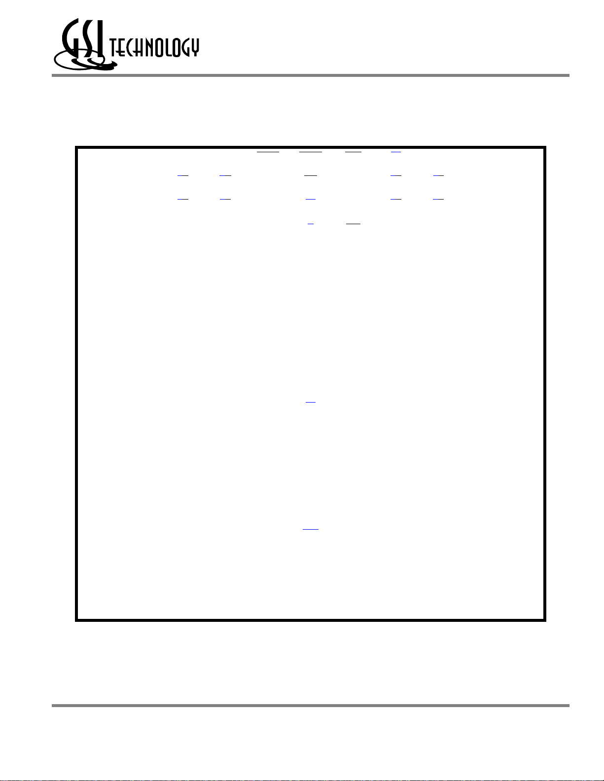
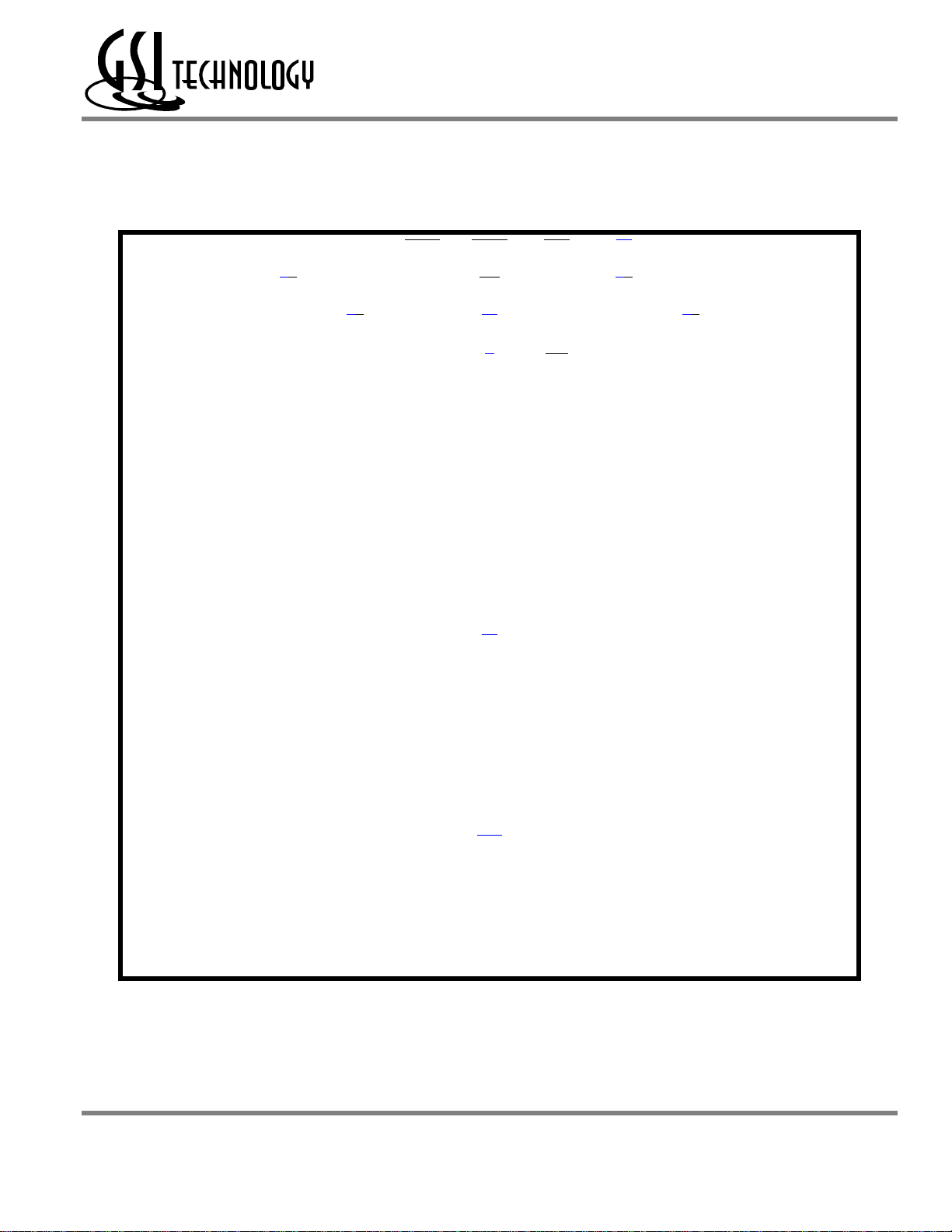
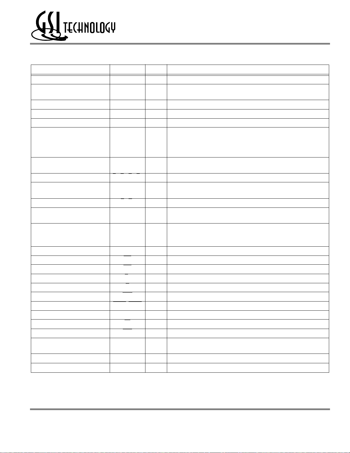
-250 -225 -200 -166 -150 -133 Unit
Pipeline
3-1-1-1
3.3 V
2.5 V
Flow
Through
2-1-1-1
3.3 V
2.5 V
t
KQ
tCycle
Curr (x18)
Curr (x36)
Curr (x72)
Curr (x18)
Curr (x36)
Curr (x72)
t
KQ
tCycle
Curr (x18)
Curr (x36)
Curr (x72)
Curr (x18)
Curr (x36)
Curr (x72)
2.3
4.0
365
560
660
360
550
640
6.0
7.0
235
300
350
235
300
340
2.5
4.4
335
510
600
330
500
590
6.5
7.5
230
300
350
230
300
340
3.0
3.5
5.0
6.0
305
265
460
400
540
460
305
260
460
390
530
450
7.5
8.51010101115ns
8.5
210
200
270
270
300
300
210
200
270
270
300
300
3.8
6.6
245
370
430
240
360
420
195
270
300
195
270
300
4.0
7.5nsns
215
mA
330
mA
380
mA
215
mA
330
mA
370
mA
150
mA
200
mA
220
mA
145
mA
190
mA
220
mA
ns
Functional Description
Applications
The GS832418/36/72 is a 37,748,736-bit high performance 2-die
synchronous SRAM module with a 2-bit burst address counter.
Although of a type originally developed for Level 2 Cache
applications supporting high performance CPUs, the device now
finds application in synchronous SRAM applications, ranging
from DSP main store to networking chip set support.
Controls
Addresses, data I/Os, chip enable (E1), address burst control
inputs (ADSP, ADSC, ADV), and write control inputs (Bx, BW,
GW) are synchronous and are controlled by a positive-edgetriggered clock input (CK). Output enable (G) and power down
control (ZZ) are asynchronous inputs. Burst cycles can be initiated
250 MHz–133MHz
2.5 V or 3.3 V V
DD
2.5 V or 3.3 V I/O
with either ADSP or ADSC inputs. In Burst mode, subsequent
burst addresses are generated internally and are controlled by
ADV. The burst address counter may be configured to count in
either linear or interleave order with the Linear Burst Order (LBO)
input. The Burst function need not be used. New addresses can be
loaded on every cycle with no degradation of chip performance.
Flow Through/Pipeline Reads
The function of the Data Output register can be controlled by the
user via the FT mode . Holding the FT mode pin low places the
RAM in Flow Through mode, causing output data to bypass the
Data Output Register. Holding FT high places the RAM in
Pipeline mode, activating the rising-edge-triggered Data Output
Register.
SCD and DCD Pipelined Reads
The GS832436(B/C) and the GS832472(C) are SCD (Single
Cycle Deselect) and DCD (Dual Cycle Deselect) pipelined
synchronous SRAMs. The GS832418(B/C) is a DCD-only
SRAM. DCD SRAMs pipeline disable commands to the same
degree as read commands. SCD SRAMs pipeline deselect
commands one stage less than read commands. SCD RAMs begin
turning off their outputs immediately after the deselect command
has been captured in the input registers. DCD RAMs hold the
deselect command for one full cycle and then begin turning off
their outputs just after the second rising edge of clock. The user
may configure the x36 or x72 versions of this SRAM for either
mode of operation using the SCD mode input.
Byte Write and Global Write
Byte write operation is performed by using Byte Write enable
(BW) input combined with one or more individual byte write
signals (Bx). In addition, Global Write (GW) is available for
writing all bytes at one time, regardless of the Byte Write control
inputs.
FLXDrive™
The ZQ pin allows selection between high drive strength (ZQ low)
for multi-drop bus applications and normal drive strength (ZQ
floating or high) point-to-point applications. See the Output Driver
Characteristics chart for details.
Sleep Mode
Low power (Sleep mode) is attained through the assertion (High)
of the ZZ signal, or by stopping the clock (CK). Memory data is
retained during Sleep mode.
Core and Interface Voltages
The GS832418/36/72 operates on a 2.5 V or 3.3 V power supply.
All input are 3.3 V and 2.5 V compatible. Separate output power
(V
) pins are used to decouple output noise from the internal
DDQ
circuits and are 3.3 V and 2.5 V compatible.
Rev: 1.00 10/2001 1/46 © 2001, Giga Semiconductor, Inc.
Specifications cited are subject to change without notice. For latest documentation see http://www.gsitechnology.com.
ByteSafe is a Trademark of Giga Semiconductor, Inc. (GSI Technology).
Preliminary
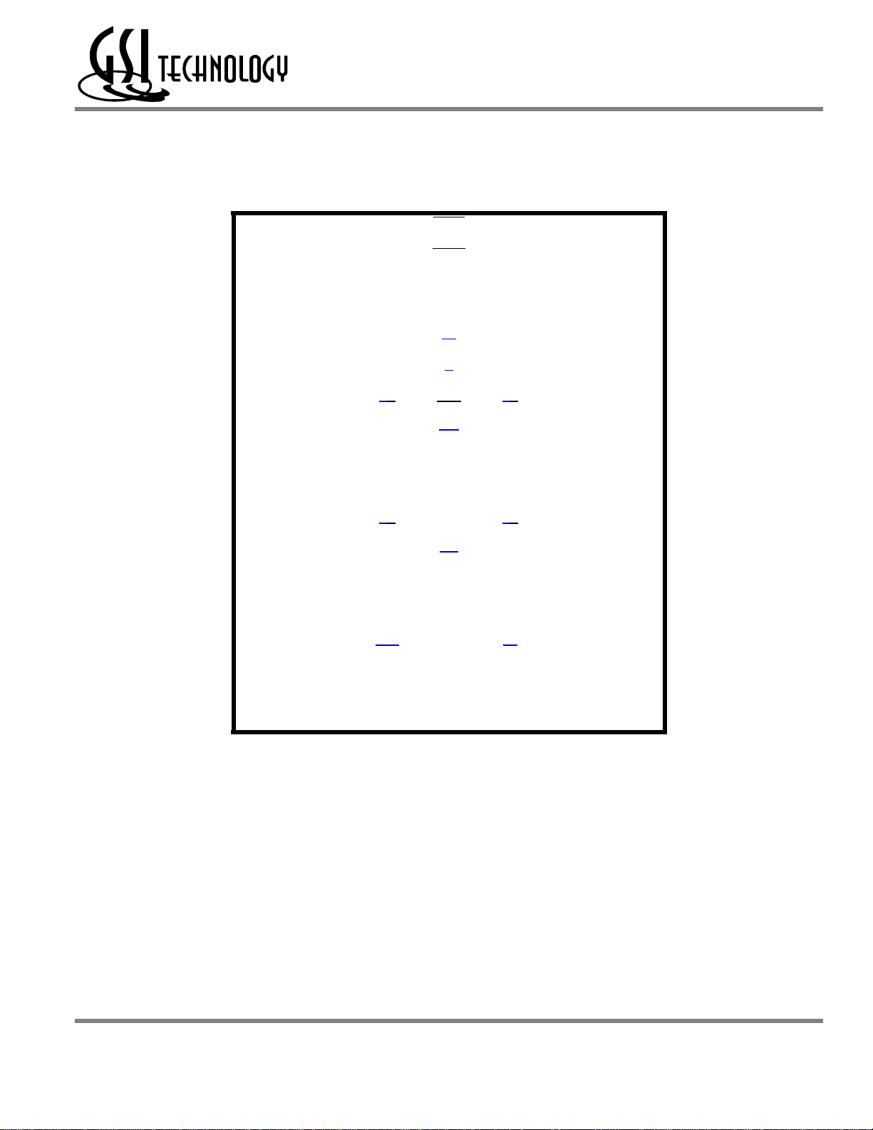
GS832418(B/C)/GS832436(B/C)/GS832472(C)
GS832472B Pad Out
209-Bump BGA—Top View
1 2 3 4 5 6 7 8 9 10 11
A DQG5 DQG1 A15 E2 ADSP ADSC ADV E3 A17 DQB1 DQB5 A
B DQG6 DQG2 BC BG NC BW A16 BB BF DQB2 DQB6 B
C DQG7 DQG3 BH BD NC E1 NC BE BA DQB3 DQB7 C
V
V
V
V
DDQ
V
DDQ
V
DDQ
SS
SS
SS
NC NC G GW NC
V
DDQ
V
V
DDQ
V
V
DDQ
D DQG8 DQG4
E DQPG9 DQPC9
F DQC4 DQC8
G DQC3 DQC7
H DQC2 DQC6
J DQC1 DQC5
K NC NC CK NC
L DQH1 DQH5
M DQH2 DQH6
N DQH3 DQH7
P DQH4 DQH8
R DQPD9 DQPH9
V
V
V
DDQ
V
DDQ
V
DDQ
SS
SS
V
V
V
DDQ
V
DDQ
V
DDQ
SS
SS
SS
SS
V
SS
V
DD
V
SS
V
DD
V
SS
V
DD
V
SS
V
DD
V
SS
V
DD
V
SS
V
DD
V
DD
ZQ
MCH
MCL
MCL
MCL
FT
MCL
SCD
ZZ
V
DD
V
DD
V
SS
V
DD
V
SS
V
DD
V
SS
V
DD
V
SS
V
DD
V
SS
V
DD
V
V
V
DDQ
V
DDQ
V
DDQ
SS
SS
V
V
V
DDQ
V
DDQ
V
DDQ
SS
SS
NC NC NC NC K
V
V
V
DDQ
V
DDQ
V
DDQ
SS
SS
V
V
V
DDQ
V
DDQ
V
DDQ
SS
SS
DQB4 DQB8 D
DQPF9 DQPB9 E
DQF8 DQF4 F
DQF7 DQF3 G
DQF6 DQF2 H
DQF5 DQF1 J
DQA5 DQA1 L
DQA6 DQA2 M
DQA7 DQA3 N
DQA8 DQA4 P
DQPA9 DQPE9 R
T DQD8 DQD4
V
SS
NC NC LBO NC NC
V
SS
DQE4 DQE8 T
U DQD7 DQD3 NC A14 A13 A12 A11 A10 A18 DQE3 DQE7 U
V DQD6 DQD2 A9 A8 A7 A1 A6 A5 A4 DQE2 DQE6 V
W DQD5 DQD1 TMS TDI A3 A0 A2 TDO TCK DQE1 DQE5 W
11 x 19 Bump BGA—14 x 22 mm2 Body—1 mm Bump Pitch
Rev: 1.00 10/2001 2/46 © 2001, Giga Semiconductor, Inc.
Specifications cited are subject to change without notice. For latest documentation see http://www.gsitechnology.com.
Preliminary
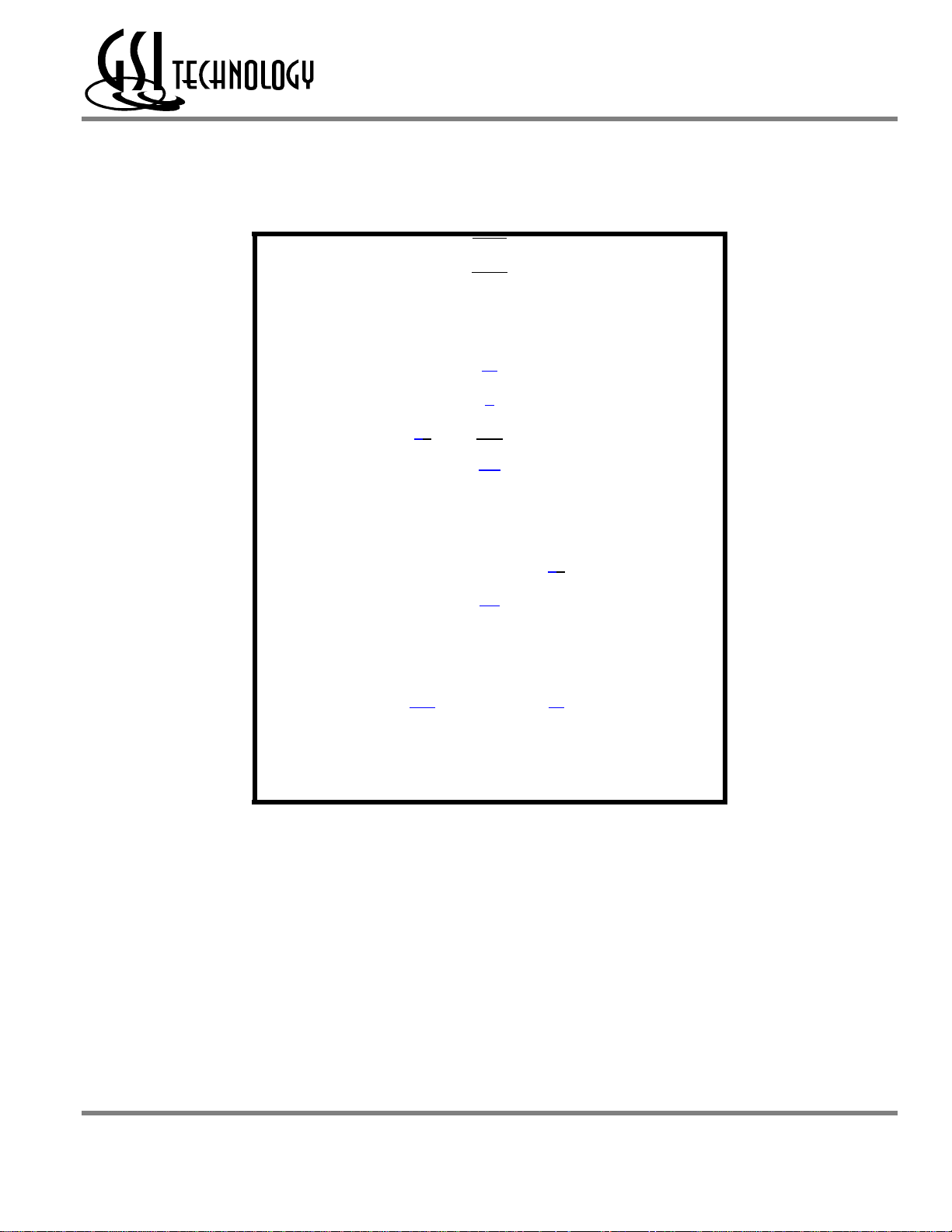
GS832418(B/C)/GS832436(B/C)/GS832472(C)
GS832436C Pad Out
209-Bump BGA—Top View
1 2 3 4 5 6 7 8 9 10 11
A NC NC A15 E2 ADSP ADSC ADV E3 A17 DQB1 DQB5 A
B NC NC BC NC A19 BW A16 BB NC DQB2 DQB6 B
C NC NC NC BD NC E1 NC NC BA DQB3 DQB7 C
V
V
V
V
DDQ
V
DDQ
V
DDQ
SS
SS
SS
NC NC G GW NC
V
DDQ
V
V
DDQ
V
V
DDQ
D NC NC
E NC DQPC9
F DQC4 DQC8
G DQC3 DQC7
H DQC2 DQC6
J DQC1 DQC5
K NC NC CK NC
L NC NC
M NC NC
N NC NC
P NC NC
R DQPD9 NC
V
V
V
DDQ
V
DDQ
V
DDQ
SS
SS
V
V
V
DDQ
V
DDQ
V
DDQ
SS
SS
SS
SS
V
SS
V
DD
V
SS
V
DD
V
SS
V
DD
V
SS
V
DD
V
SS
V
DD
V
SS
V
DD
V
DD
ZQ
MCH
MCL
MCL
MCL
FT
MCL
SCD
ZZ
V
DD
V
DD
V
SS
V
DD
V
SS
V
DD
V
SS
V
DD
V
SS
V
DD
V
SS
V
DD
V
V
V
DDQ
V
DDQ
V
DDQ
SS
SS
V
V
V
DDQ
V
DDQ
V
DDQ
SS
SS
NC NC NC NC K
V
V
V
DDQ
V
DDQ
V
DDQ
SS
SS
V
V
V
DDQ
V
DDQ
V
DDQ
SS
SS
DQB4 DQB8 D
NC DQPB9 E
NC NC F
NC NC G
NC NC H
NC NC J
DQA5 DQA1 L
DQA6 DQA2 M
DQA7 DQA3 N
DQA8 DQA4 P
DQPA9 NC R
T DQD8 DQD4
V
SS
NC NC LBO NC NC
V
SS
NC NC T
U DQD7 DQD3 NC A14 A13 A12 A11 A10 A18 NC NC U
V DQD6 DQD2 A9 A8 A7 A1 A6 A5 A4 NC NC V
W DQD5 DQD1 TMS TDI A3 A0 A2 TDO TCK NC NC W
11 x 19 Bump BGA—14 x 22 mm2 Body—1 mm Bump Pitch
Rev: 1.00 10/2001 3/46 © 2001, Giga Semiconductor, Inc.
Specifications cited are subject to change without notice. For latest documentation see http://www.gsitechnology.com.

Preliminary
GS832418(B/C)/GS832436(B/C)/GS832472(C)
GS832418C Pad Out
209-Bump BGA—Top View
1 2 3 4 5 6 7 8 9 10 11
A NC NC A15 MCH ADSP ADSC ADV MCL A17 NC NC A
B NC NC BB NC A19 BW A16 NC NC NC NC B
C NC NC NC NC NC E1 A20 NC BA NC NC C
V
V
V
V
DDQ
V
DDQ
V
DDQ
SS
SS
SS
NC NC G GW NC
V
DDQ
V
V
DDQ
V
V
DDQ
D NC NC
E NC DQPB9
F DQB4 DQB8
G DQB3 DQB7
H DQB2 DQB6
J DQB1 DQB5
K NC NC CK NC
L NC NC
M NC NC
N NC NC
P NC NC
R NC NC
V
V
V
DDQ
V
DDQ
V
DDQ
SS
SS
V
V
V
DDQ
V
DDQ
V
DDQ
SS
SS
SS
SS
V
SS
V
DD
V
SS
V
DD
V
SS
V
DD
V
SS
V
DD
V
SS
V
DD
V
SS
V
DD
V
DD
ZQ
MCH
MCL
MCL
MCL
FT
MCL
MCL
ZZ
V
DD
V
DD
V
SS
V
DD
V
SS
V
DD
V
SS
V
DD
V
SS
V
DD
V
SS
V
DD
V
V
V
DDQ
V
DDQ
V
DDQ
SS
SS
V
V
V
DDQ
V
DDQ
V
DDQ
SS
SS
NC NC NC NC K
V
V
V
DDQ
V
DDQ
V
DDQ
SS
SS
V
V
V
DDQ
V
DDQ
V
DDQ
SS
SS
NC NC D
NC NC E
NC NC F
NC NC G
NC NC H
NC NC J
DQA5 DQA1 L
DQA6 DQA2 M
DQA7 DQA3 N
DQA8 DQA4 P
DQPA9 NC R
T NC NC
V
SS
NC NC LBO NC NC
V
SS
NC NC T
U NC NC NC A14 A13 A12 A11 A10 A18 NC NC U
V NC NC A9 A8 A7 A1 A6 A5 A4 NC NC V
W NC NC TMS TDI A3 A0 A2 TDO TCK NC NC W
11 x 19 Bump BGA—14 x 22 mm2 Body—1 mm Bump Pitch
Rev: 1.00 10/2001 4/46 © 2001, Giga Semiconductor, Inc.
Specifications cited are subject to change without notice. For latest documentation see http://www.gsitechnology.com.
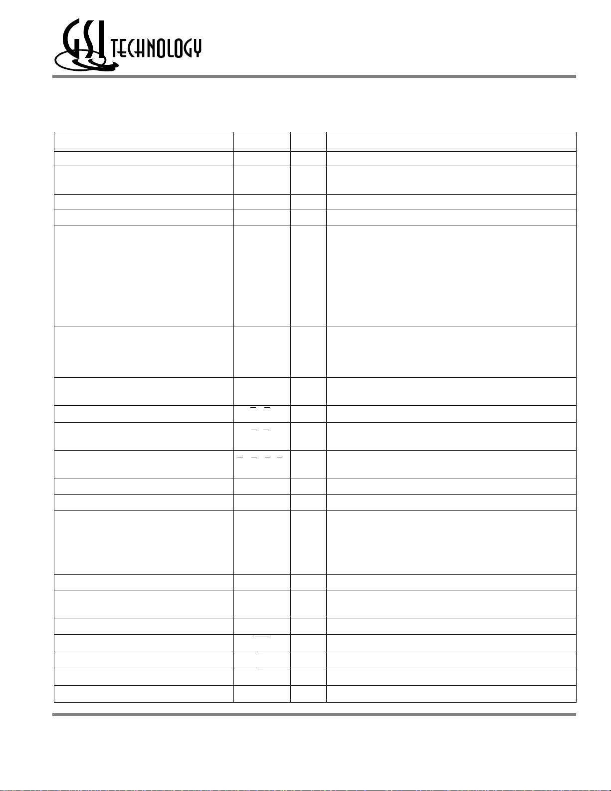
GS832418/36/72 209-Bump BGA Pin Description
Pin Location Symbol Type Description
W6, V6 A0, A1 I Address field LSBs and Address Counter Preset Inputs.
W7, W5, V9, V8, V7, V5, V4, V3, U8, U7, U6,
U5, U4, A3, B7, A9, U9
B5 A19 I Address Inputs (x36/x18 Versions)
C7 A20 I Address Inputs (x18 Version)
L11, M11, N11, P11, L10, M10, N10, P10, R10
A10, B10, C10, D10, A11, B11, C11, D11, E11
J1, H1, G1, F1, J2, H2, G2, F2, E2
W2, V2, U2, T2, W1, V1, U1, T1, R1
W10, V10, U10, T10, W11, V11, U11, T11, R11
J11, H11, G11, F11, J10, H10, G10, F10, E10
A2, B2, C2, D2, A1, B1, C1, D1, E1
L1, M1, N1, P1, L2, M2, N2, P2, R2
L11, M11, N11, P11, L10, M10, N10, P10, R10
A10, B10, C10, D10, A11, B11, C11, D11, E11
J1, H1, G1, F1, J2, H2, G2, F2, E2
W2, V2, U2, T2, W1, V1, U1, T1, R1
L11, M11, N11, P11, L10, M10, N10, P10, R10
J1, H1, G1, F1, J2, H2, G2, F2, E2
C9, B8
B3, C4
C8, B9, B4, C3
B5 NC — No Connect (x72 Version)
C7 NC — No Connect (x72/x36 Versions)
W10, V10, U10, T10, W11, V11, U11, T11, R11
J11, H11, G11, F11, J10, H10, G10, F10, E10
A2, B2, C2, D2, A1, B1, C1, D1, E1
L1, M1, N1, P1, L2, M2, N2, P2, R2, C8, B9,
B4, C3
B3, C4 NC — No Connect (x18 Version)
C5, D4, D5, D8, K1, K2, K4, K8, K9, K10, K11,
T4, T5, T7, T8, U3
K3 CK I Clock Input Signal; active high
D7
C6
A8
A4
An I Address Inputs
DQA1–DQA9
DQB1–DQB9
DQC1–DQC9
DQD1–DQD9
DQE1–DQE9
DQF1–DQF9
DQG1–DQG9
DQH1–DQH9
DQA1–DQA9
DQB1–DQB9
DQC1–DQC9
DQD1–DQD9
DQA1–DQA9
DQB1–DQB9
BA, BB
BC,BD
BE, BF, BG,BH
NC — No Connect (x36/x18 Versions)
NC — No Connect
GW
E1
E3
E2
I/O Data Input and Output pins (x72 Version)
I/O Data Input and Output pins (x36 Version)
I/O Data Input and Output pins (x18 Version)
Preliminary
GS832418(B/C)/GS832436(B/C)/GS832472(C)
I Byte Write Enable for DQA, DQB I/Os; active low
I
I
I Global Write Enable—Writes all bytes; active low
I Chip Enable; active low
I Chip Enable; active low (x72/x36 Versions)
I Chip Enable; active high (x72/x36 Versions)
Byte Write Enable for DQC, DQD I/Os; active low
(x72/x36 Versions)
Byte Write Enable for DQE, DQF, DQG, DQH I/Os; active low
(x72 Version)
Rev: 1.00 10/2001 5/46 © 2001, Giga Semiconductor, Inc.
Specifications cited are subject to change without notice. For latest documentation see http://www.gsitechnology.com.
GS832418/36/72 209-Bump BGA Pin Description
Pin Location Symbol Type Description
Preliminary
GS832418(B/C)/GS832436(B/C)/GS832472(C)
D6
A7
A5, A6
P6
L6
T6
N6
G6
A4
H6, J6, K6, M6
A8, N6
B6
F6
W3
W4
W8
W9
E5, E6, E7, G5, G7, J5, J7, L5, L7, N5, N7, R5,
R6, R7
D3, D9, F3, F4, F5, F7, F8, F9, H3, H4, H5, H7,
H8, H9, K5, K7, M3, M4, M5, M7, M8, M9, P3,
P4, P5, P7, P8, P9, T3, T9
E3, E4, E8, E9, G3, G4, G8, G9, J3, J4, J8, J9,
L3, L4, L8, L9, N3, N4, N8, N9, R3, R4, R8, R9
G
ADV
ADSP, ADSC
ZZ
FT
LBO
SCD
MCH
MCH
MCL
MCL
BW
ZQ
TMS
TDI
TDO
TCK
V
DD
V
SS
V
DDQ
I Output Enable; active low
I Burst address counter advance enable; active low
I Address Strobe (Processor, Cache Controller); active low
I Sleep Mode control; active high
I Flow Through or Pipeline mode; active low
I Linear Burst Order mode; active low
I
I Must Connect High
I Must Connect High (x18 version)
I Byte Enable; active low
I
I Scan Test Mode Select
I Scan Test Data In
O Scan Test Data Out
I Scan Test Clock
I Core power supply
I I/O and Core Ground
I Output driver power supply
Single Cycle Deselect/Dual Cycle Deselect Mode Control (
x72/x36 Versions)
Must Connect Low
Must Connect Low (x18 version)
FLXDrive Output Impedance Control
(Low = Low Impedance [High Drive], High = High Impedance [Low
Drive])
Rev: 1.00 10/2001 6/46 © 2001, Giga Semiconductor, Inc.
Specifications cited are subject to change without notice. For latest documentation see http://www.gsitechnology.com.
GS832418(B/C)/GS832436(B/C)/GS832472(C)
GS832436B Pad Out
119-Bump BGA—Top View
1 2 3 4 5 6 7
Preliminary
A V
DDQ
A6 A7 ADSP A8 A9 V
DDQ
B NC A18 A4 ADSC A15 A17 NC B
C NC A5 A3 V
D DQC4 DQPC9 V
E DQC3 DQC8 V
F V
DDQ
DQC7 V
SS
SS
SS
DD
ZQ V
E1 V
G V
A14 A16 NC C
SS
SS
SS
DQPB9 DQB4 D
DQB8 DQB3 E
DQB7 V
DDQ
G DQC2 DQC6 BC ADV BB DQB6 DQB2 G
H DQC1 DQC5 V
J V
DDQ
V
DD
K DQD1 DQD5 V
SS
NC V
SS
GW V
DD
CK V
SS
NC V
SS
DQB5 DQB1 H
DD
V
DDQ
DQA5 DQA4 K
L DQD2 DQD6 BD SCD BA DQA6 DQA3 L
M V
DDQ
N DQD3 DQD8 V
P DQD4 DQPD9 V
DQD7 V
SS
SS
SS
BW V
A1 V
A0 V
SS
SS
SS
DQA7 V
DDQ
DQA8 DQA2 N
DQPA9 DQA1 P
A
F
J
M
R NC A2 LBO V
DD
FT A13 NC R
T NC NC A10 A11 A12 A19 ZZ T
U V
DDQ
TMS TDI TCK TDO NC V
DDQ
U
7 x 17 Bump BGA—14 x 22 mm2 Body—1.27 mm Bump Pitch
Rev: 1.00 10/2001 7/46 © 2001, Giga Semiconductor, Inc.
Specifications cited are subject to change without notice. For latest documentation see http://www.gsitechnology.com.
GS832418(B/C)/GS832436(B/C)/GS832472(C)
GS832418B Pad Out
119-Bump BGA—Top View
1 2 3 4 5 6 7
Preliminary
A V
DDQ
A6 A7 ADSP A8 A9 V
DDQ
B NC A18 A4 ADSC A15 A17 NC B
C NC A5 A3 V
D DQB1 NC V
E NC DQB2 V
F V
DDQ
NC V
SS
SS
SS
DD
ZQ V
E1 V
G V
A14 A16 NC C
SS
SS
SS
DQPA9 NC D
NC DQA8 E
DQA7 V
DDQ
G NC DQB3 BB ADV NC NC DQA6 G
H DQB4 NC V
J V
DDQ
V
DD
K NC DQB5 V
SS
NC V
SS
L DQB6 NC NC V
M V
DDQ
N DQB8 NC V
P NC DQPB9 V
DQB7 V
SS
SS
SS
GW V
DD
CK V
SS
BW V
A1 V
A0 V
SS
NC V
SS
DQA5 NC H
DD
V
DDQ
NC DQA4 K
BA DQA3 NC L
SS
SS
SS
NC V
DDQ
DQA2 NC N
NC DQA1 P
A
F
J
M
R NC A2 LBO V
DD
FT A13 NC R
T NC A10 A11 A20 A12 A19 ZZ T
U V
DDQ
TMS TDI TCK TDO NC V
DDQ
U
7 x 17 Bump BGA—14 x 22 mm2 Body—1.27 mm Bump Pitch
Rev: 1.00 10/2001 8/46 © 2001, Giga Semiconductor, Inc.
Specifications cited are subject to change without notice. For latest documentation see http://www.gsitechnology.com.
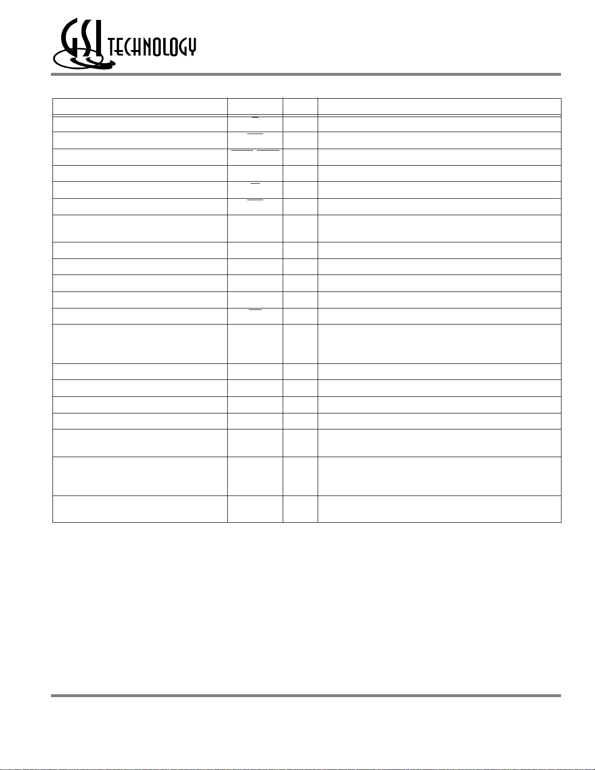
GS832418/36 119-Bump BGA Pin Description
Pin Location Symbol Type Description
P4, N4 A0, A1 I Address field LSBs and Address Counter Preset Inputs
R2, C3, B3, C2, A2, A3, A5, A6, T3,
T5, R6, C5, B5, C6, B6, B2
T4, T6 An Address Input (x36 Version)
T2 NC — No Connect (x36 Version)
T2, T6, T4 An I Address Input (x18 Version)
K7, L7, N7, P7, K6, L6, M6, N6
H7, G7, E7, D7, H6, G6, F6, E6
H1, G1, E1, D1, H2, G2, F2, E2
K1, L1, N1, P1, K2, L2, M2, N2
P6, D6, D2, P2
L5, G5, G3, L3 BA, BB, BC, BD I Byte Write Enable for DQA, DQB, DQC, DQD I/Os; active low (x36 Version)
P7, N6, L6, K7, H6, G7, F6, E7, D6
D1, E2, G2, H1, K2, L1, M2, N1, P2
L5, G3 BA, BB I Byte Write Enable for DQA, DQB I/Os; active low (x18 Version)
B1, C1, R1, T1, U6, B7, C7, J3, J5,
R7
P6, N7, M6, L7, K6, H7, G6, E6, D7,
D2, E1, F2, G1, H2, K1, L2, N2, P1,
G5, L3
K4 CK I Clock Input Signal; active high
M4 BW I Byte Write—Writes all enabled bytes; active low
H4 GW I Global Write Enable—Writes all bytes; active low
E4 E1 I Chip Enable; active low
F4 G I Output Enable; active low
G4 ADV I Burst address counter advance enable; active low
A4, B4 ADSP, ADSC I Address Strobe (Processor, Cache Controller); active low
T7 ZZ I Sleep mode control; active high
R5 FT I Flow Through or Pipeline mode; active low
R3 LBO I Linear Burst Order mode; active low
D4 ZQ I
L4 SCD I Single Cycle Deselect/Dual Cyle Deselect Mode Control (x36 version)
U2
An I Address Inputs
DQA1–DQA8
DQB1–DQB8
DQC1–DQC8
DQD1–DQD8
DQA9, DQB9,
DQC9, DQD9
DQA1–DQA9
DQB1–DQB9
NC — No Connect
NC — No Connect (x18 Version)
TMS
I/O Data Input and Output pins. (x36 Version)
I/O Data Input and Output pins. (x36 Version)
I/O Data Input and Output pins (x18 Version)
I Scan Test Mode Select
Preliminary
GS832418(B/C)/GS832436(B/C)/GS832472(C)
FLXDrive Output Impedance Control (Low = Low Impedance [High Drive],
High = High Impedance [Low Drive])
Rev: 1.00 10/2001 9/46 © 2001, Giga Semiconductor, Inc.
Specifications cited are subject to change without notice. For latest documentation see http://www.gsitechnology.com.
GS832418/36 119-Bump BGA Pin Description
Pin Location Symbol Type Description
Preliminary
GS832418(B/C)/GS832436(B/C)/GS832472(C)
U3
U5
U4
J2, C4, J4, R4, J6
D3, E3, F3, H3, K3, M3, N3, P3, D5,
E5, F5, H5, K5, M5, N5, P5
L4
A1, F1, J1, M1, U1, A7, F7, J7, M7,
U7
TDI
TDO
TCK
V
V
V
V
DDQ
DD
SS
SS
I Scan Test Data In
O Scan Test Data Out
I Scan Test Clock
I Core power supply
I I/O and Core Ground
I I/O and Core Ground
I Output driver power supply
Rev: 1.00 10/2001 10/46 © 2001, Giga Semiconductor, Inc.
Specifications cited are subject to change without notice. For latest documentation see http://www.gsitechnology.com.
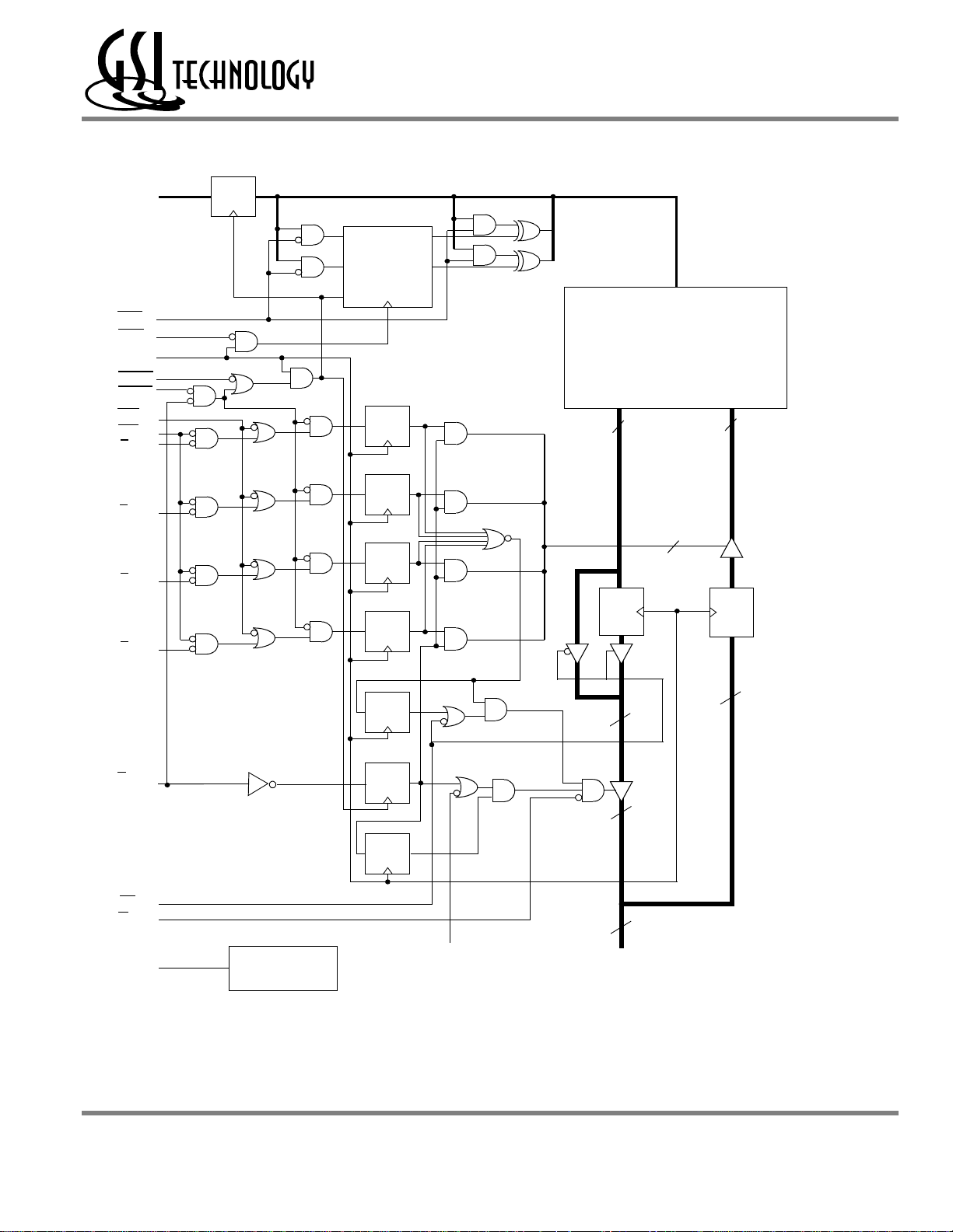
GS832418/36/72 Block Diagram
Preliminary
GS832418(B/C)/GS832436(B/C)/GS832472(C)
A0–An
LBO
ADV
CK
ADSC
ADSP
GW
BW
BA
BB
BC
BD
Register
D Q
A0
A1
D0
D1
Counter
Load
Register
D Q
Register
D Q
Register
D Q
Register
D Q
Q0
Q1
A0
A1
A
Memory
Array
Q D
36
4
DQ
Register
36
Register
DQ
E1
FT
G
ZZ
Note: Only x36 version shown for simplicity.
Power Down
Control
Register
D Q
Register
D Q
Register
D Q
SCD
36
36
36
DQx0–DQx9
36
Rev: 1.00 10/2001 11/46 © 2001, Giga Semiconductor, Inc.
Specifications cited are subject to change without notice. For latest documentation see http://www.gsitechnology.com.
Preliminary
GS832418(B/C)/GS832436(B/C)/GS832472(C)
GS832418 Die Layout
GS832436 Die Layout
Die A
x18
16Mb
Die A
x18
16Mb
Inputs
TDO TDI TDOTDI
Die B
x18
16Mb
18 I/Os
Inputs
TDO TDI TDOTDI
Die B
x18
16Mb
18 I/Os 18 I/Os
GS832472 Die Layout
Inputs
Die A
TDO TDI TDOTDI
x36
32Mb
36 I/Os 36 I/Os
Rev: 1.00 10/2001 12/46 © 2001, Giga Semiconductor, Inc.
Specifications cited are subject to change without notice. For latest documentation see http://www.gsitechnology.com.
Die B
x36
32Mb
Linear Burst Sequence
I
Mode Pin Functions
Preliminary
GS832418(B/C)/GS832436(B/C)/GS832472(C)
Mode Name
Burst Order Control LBO
Output Register Control FT
Power Down Control ZZ
Single/Dual Cycle Deselect Control SCD
FLXDrive Output Impedance Control ZQ
Note:
There are pull-up devices on the ZQ, SCD and FT pins and a pull-down device on the ZZ pin, so those input pins can be unconnected and the
chip will operate in the default states as specified in the above tables.
Pin
Name
State Function
L Linear Burst
H Interleaved Burst
L Flow Through
H or NC Pipeline
L or NC Active
H
L Dual Cycle Deselect
H or NC Single Cycle Deselect
L High Drive (Low Impedance)
H or NC Low Drive (High Impedance)
Standby, IDD = I
SB
Enable / Disable Parity I/O Pins
This SRAM allows the user to configure the device to operate in Parity I/O active (x18, x36, or x72) or in Parity I/O inactive (x16,
x32, or x64) mode. Holding the PE bump low or letting it float will activate the 9th I/O on each byte of the RAM. Grounding PE
deactivates the 9th I/O of each byte, although the bit in each byte of the memory array remains active to store and recall parity bits
generated and read into the ByteSafe parity circuits.
Burst Counter Sequences
nterleaved Burst Sequence
A[1:0] A[1:0] A[1:0] A[1:0]
1st address 00 01 10 11
2nd address 01 10 11 00
3rd address 10 11 00 01
4th address 11 00 01 10
Note: The burst counter wraps to initial state on the 5th clock.
Rev: 1.00 10/2001 13/46 © 2001, Giga Semiconductor, Inc.
Specifications cited are subject to change without notice. For latest documentation see http://www.gsitechnology.com.
1st address 00 01 10 11
2nd address 01 00 11 10
3rd address 10 11 00 01
4th address 11 10 01 00
Note: The burst counter wraps to initial state on the 5th clock.
A[1:0] A[1:0] A[1:0] A[1:0]
BPR 1999.05.18
GS832418(B/C)/GS832436(B/C)/GS832472(C)
Byte Write Truth Table
Function GW BW BA BB BC BD Notes
Read H H X X X X 1
Read H L H H H H 1
Write byte a H L L H H H 2, 3
Write byte b H L H L H H 2, 3
Write byte c H L H H L H 2, 3, 4
Write byte d H L H H H L 2, 3, 4
Write all bytes H L L L L L 2, 3, 4
Write all bytes L X X X X X
Notes:
1. All byte outputs are active in read cycles regardless of the state of Byte Write Enable inputs.
2. Byte Write Enable inputs BA, BB, BC, and/or BD may be used in any combination with BW to write single or multiple bytes.
3. All byte I/Os remain High-Z during all write operations regardless of the state of Byte Write Enable inputs.
4. Bytes “C” and “D” are only available on the x36 version.
Preliminary
Rev: 1.00 10/2001 14/46 © 2001, Giga Semiconductor, Inc.
Specifications cited are subject to change without notice. For latest documentation see http://www.gsitechnology.com.
 Loading...