

GSI GS820V32T, GS820V32Q Datasheet
G S I T E C H N O L O G Y
GS820V32Q/T
GS820V32Q/T
4/5/6, 2.5V I/O, 2.0mA
64K x 32 Burst
Features
• Single 3.3V +5%/-5% power supply
• Separate VDDQ to allow 2.375V to 3.465V output supply level
• High frequency operation: 117MHz
• Fast access time: 4.5ns Clock to Q
• Low power: 0.5mA ISB and IDD static
• FT mode pin for either flow-thru or pipeline operation
• LBO mode pin for linear or interleave (Pentium
burst mode
TM
and X86)
• Byte write (BWE) and global write (GW) operation
• 3 chip enable signals for easy depth expansion
• 2 cycles enable (pipeline mode) and 1 cycle disable to allow multiple
bank without data buss contention
• Compatible to both 3.3V and 2.5V interface level
• Standard Industrial Temperature Option: -40 to +85C
• JEDEC standard 100 lead package:
Q: QFP
T: TQFP
Pentium is a trademark of Intel Corp.
Functional Description
The GS820V32 is a 64Kx32 high performance synchronous SRAM
with 2 bit burst counter. It is designed to provide L2 Cache for PentiumTM and other high performance CPU. Addresses (A0-15), data
IOs (DQ1-32), chip enables (CE1, CE2, CE3), address control inputs
(ADSP, ADSC, ADV) and write control inputs (BW1, BW2, BW3,
BW4, BWE, GW) are synchronous and are controlled by a positive
edge triggered clock (CLK).
80-133MHz (P/L)
66MHz Flow-Thru
Output enable (OE) and power down control (ZZ) are asynchronous. 2 mode control pins (LBO & FT) define 4 operation modes
of linear/interleave burst order and output flow-thru/pipeline.
Burst can be initiated with either ADSP or ADSC inputs. Subsequent burst address are generated internally and are controlled by
ADV. The burst sequence is either interleave order (Pentium
and X86) or linear order and is defined by LBO.
Output registers are provided and are controlled by FT mode pin.
With FT mode pin, Output registers can be programmed in either
pipeline mode for very high frequency operation (117MHz) or
flow-thru mode for reduced latency.
Byte write operation can be obtained through byte write enable
(BWE) input combined with 4 individual byte write signals
BW1-4. In addition, global write (GW) signal is also available to
write all bytes at once.
Low power state (standby mode) can be obtained either through
the assertion of ZZ signal or simply stop the clock (CLK). In
standby mode, memory data are still retained. Low power design
of 0.5mA standby are provided on L version.
The GS820V32 operates from a 3.3V power supply and all
inputs and outputs are LVTTL compatible. Separate output
power (VDDQ) and ground (VSSQ) pins are employed to decouple output noise from internal circuit and VDDQ allow user
the flexibility to employ lower output supply level like 2.5V.
GS820V32’s interface level is also compatble to 2.5V supply
level.
The GS820V32 is implemented with GSI’s high performance
CMOS technology and is available in JEDEC standard 100 lead
QFP ( Q version ) and TQFP ( T version) package.
TM
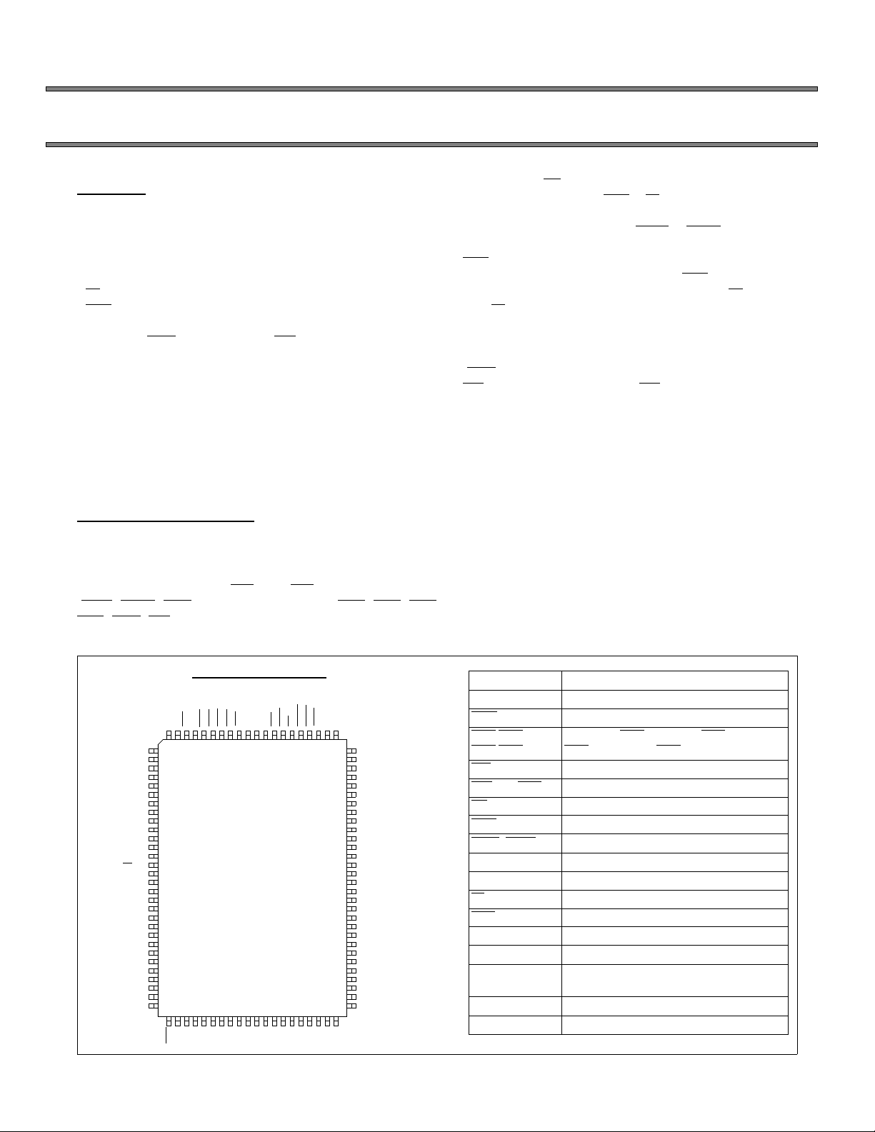
Pin configuration
Top view
A6
A7
CE1
CE2
100 99 98 97 96 95 94 93 92 91 90 89 88 87 86 85 84 83 82 81
NC
1
DQ17
2
DQ18
3
VDDQ
4
VSSQ
5
DQ19
6
DQ20
7
DQ21
8
DQ22
9
VSSQ
10
11
VDDQ
12
DQ23
13
DQ24
14
FT
15
VDD
NC
16
VSS
17
DQ25
18
DQ26
19
VDDQ
20
VSSQ
21
22
DQ27
23
DQ28
24
DQ29
25
DQ30
26
VSSQ
27
VDDQ
28
DQ31
29
DQ32
30
NC
31 32 33 34 35 36 37 38 39 40 41 42 43 44 45 46 47 48 49 50
LBOA5A4
A3A2A1A0NC
Rev. 9/09/97 1/15
CE3
VDD
BW2
BW1
BW3
BW4
GW
BWE
VSS
OE
CLK
100 pin QFP / TQFP
NC
NC
VSS
NC
A10
A11
VDD
ADVA8A9
ADSP
ADSC
NC
80
DQ16
79
DQ15
78
VDDQ
77
VSSQ
76
DQ14
75
DQ13
74
DQ12
73
DQ11
72
71
VSSQ
70
VDDQ
69
DQ10
68
DQ9
67
VSS
66
NC
65
VDD
64
ZZ
63
DQ8
DQ7
62
61
VDDQ
60
VSSQ
59
DQ6
58
DQ5
57
DQ4
56
DQ3
55
VSSQ
54
VDDQ
53
DQ2
52
DQ1
51
NC
NC
A13
A15
A12
A14
A0-15 Address Inputs
CLK Clock Input
BWE Byte Write Enable
BW1,BW2
BW3,BW4
Byte Write. BW1 for DQ1-8; BW2 for DQ9-16;
BW3 for DQ17-24; BW4 for DQ25-32
GW Global Write Enable
CE1,CE2, CE3 Chip Enable
OE Output Enable
ADV Burst Address advance
ADSP, ADSC Address Status
DQ1-32 Data I/O
ZZ Power down control
FT Flow-Thru mode
LBO Linear Burst mode
VDD 3.3V Power Supply
VSS Ground
VDDQ Output Power Supply, 2.375V to VDD
(3.465Vmax)
VSSQ Output Ground
NC No Connect
G S I T E C H N O L O G Y
GS820V32Q/T
GS820V32Q/T
4/5/6, 2.5V I/O, 2.0mA
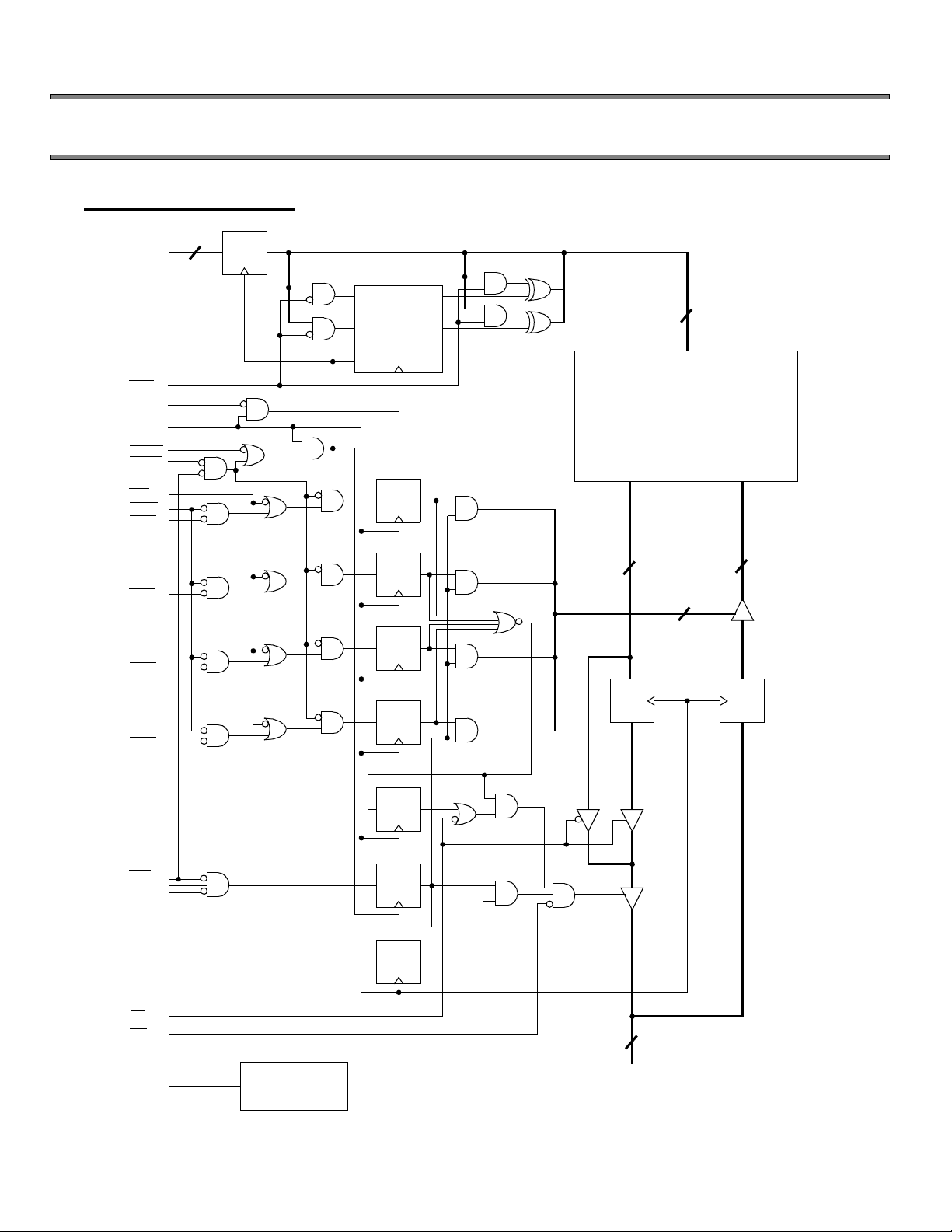
Functional Block Diagram
16
A0-15
LBO
ADV
CLK
ADSC
ADSP
GW
BWE
BW1
BW2
Register
D Q
64K x 32 Burst
Q0
Q1
A0
A1
A0
A1
D0
D1
Load
Binary
Counter
Register
D Q
Register
D Q
16
A
64Kx32
Memory
Array
Q D
32
4
80-133MHz (P/L)
66MHz Flow-Thru
32
BW3
BW4
CE1
CE2
CE3
FT
OE
ZZ
Powerdown
Control
Register
D Q
Register
D Q
Register
D Q
Register
D Q
Register
D Q
DQ
Register
32
DQ1-32
Register
DQ
Rev. 9/09/97 2/15
G S I T E C H N O L O G Y
GS820V32Q/T
GS820V32Q/T
4/5/6, 2.5V I/O, 2.0mA
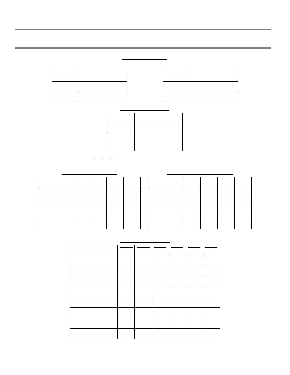
LBO Function
L Linear Burst
H or NC Interleaved Burst
Note: There are pull up devices on LBO and FT pins and pull down device on ZZ pin, so those input pins can be unconnected and
the chip will operate in the default states as specified in the above tables.
Linear Burst sequence
64K x 32 Burst
Mode pin function
FT Function
L Flow-Thru
H or NC Pipeline
Power down control
ZZ Function
L or NC Active
H Standby
IDD=ISB
Interleaved Burst sequence
80-133MHz (P/L)
66MHz Flow-Thru
A[1:0] A[1:0] A[1:0] A[1:0]
1st address 00 01 10 11
2nd address 01 10 11 00
3rd address 10 11 00 01
4th address 11 00 01 10
The burst wrap around to initial state upon completion
Byte Write Function
Function SGW BWE BW1 BW2 BW3 BW4
Read H H X X X X
Read H L H H H H
Write all bytes L X X X X X
Write all bytes H L L L L L
Write byte 1 H L L H H H
Write byte 2 H L H L H H
A[1:0] A[1:0] A[1:0] A[1:0]
1st address 00 01 10 11
2nd address 01 00 11 10
3rd address 10 11 00 01
4th address 11 10 01 00
The burst wrap around to initial state upon completion
Write byte 3 H L H H L H
Write byte 4 H L H H H L
Note: H=logic high, L=logic low, NC= no connect
Rev. 9/09/97 3/15
G S I T E C H N O L O G Y
GS820V32Q/T
GS820V32Q/T
4/5/6, 2.5V I/O, 2.0mA
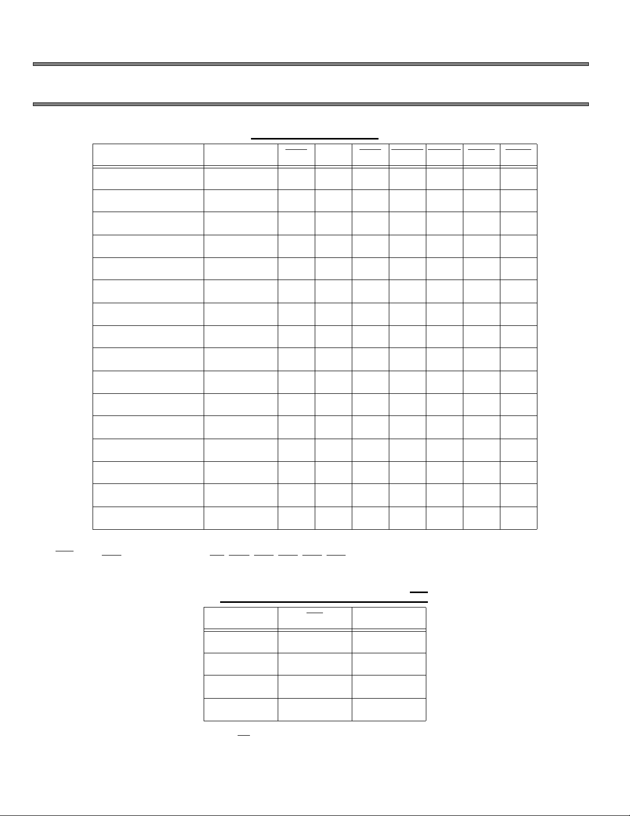
Cycle Address used CE1 CE2 CE3 ADSP ADSC ADV BWx
Deselect none H X X X L X X
Deselect none L L X X L X X
Deselect none L X H X L X X
Deselect none L L X L X X X
Deselect none L X H L X X X
Read, begin burst external L H L L X X X
Read, begin burst external L H L H L X H
Read, continue burst next X X X H H L H
Read, continue burst next H X X X H L H
64K x 32 Burst
Synchronous truth table
80-133MHz (P/L)
66MHz Flow-Thru
Read, suspend burst current X X X H H H H
Read, suspend burst current H X X X H H H
Write, begin burst external L H L H L X L
Write, continue burst next X X X H H L L
Write, continue burst next H X X X H L L
Write, suspend burst current X X X H H H L
Write, suspend burst current H X X X H H L
Note: 1. X=don’t care, H=logic high, L=logic low
2. BWx is the logic function of GW, BWE, BW1, BW2, BW3, BW4. See Byte Write Function table for detail.
3. All inputs in the table must meet setup and hold on rising edge of CLK.
DQ Bus Control and Asynchronous OE
Cycle OE DQ
Read L Q
Read H Hi-Z
Write X Hi-Z; D
Deselect X Hi-Z
Note: On the write cycle that follows read cycle, OE need to be held high prior to the start of write cycle to tri-state DQ buss and allow data
input to SRAM.
Rev. 9/09/97 4/15
G S I T E C H N O L O G Y
GS820V32Q/T
GS820V32Q/T
4/5/6, 2.5V I/O, 2.0mA
Absolute Maximum Ratings (Voltage reference to VSS=0V)
Parameter Symbol Rating Unit
Supply Voltage VDD -0.5 to 4.6 V
Output Supply Voltage VDDQ -0.5 to VDD V
CLK Input Voltage VCLK -0.5 to 6 V
Input Voltage VIN -0.5 to VDD+0.5
Output Voltage VOUT -0.5 to VDD+0.5
Power Dissipation PD 1.5 W
Operating Temperature Topr 0 to 70
Storage Temperature Tstg -55 to 150
64K x 32 Burst
(≤ 4.6 V max. )
(≤ 4.6 V max. )
80-133MHz (P/L)
66MHz Flow-Thru
V
V
o
C
o
C
Note: Permanent device damage may occur if Absolute Maximum Ratings are exceeded. Functional operation should be
restricted to Recommended Operating Conditions. Exposure to higher than recommended voltages for extended periods
of time could affect device reliability.
Recommended Operating Conditions (Voltage reference to VSS=0V)
(VDD=3.135V to 3.465V, Ta=0 70C)
Parameter Symbol Min. Typ. Max. Unit
Supply Voltage VDD 3.135 3.3 3.465 V
Output Supply Voltage VDDQ 2.375 3.3 3.465 V
Input High Voltage VIH 1.7 --- VDD+0.3 V
Input Low Voltage VIL -0.3 --- 0.8 V
Note: Input overshoot voltage should be less than VDD+2V and not exceed 5ns.
Input undershoot voltage should be higher than -2V and not exceed 5ns.
Capacitance ( Ta=25C, f=1MHz)
Parameter Symbol Test conditions Typ. Max. Unit
Input Capacitance CIN VIN=0V 4 5 pF
Output Capacitance COUT VOUT=0V 6 7 pF
Note: These parameters are sampled and are not 100% tested.
Rev. 9/09/97 5/15
 Loading...