

GSI GS820E32T-6I, GS820E32T-6, GS820E32T-5I, GS820E32T-5, GS820E32T-4I Datasheet
...
GS820E32T/Q-150/138/133/117/100/66
TQFP, QFP
64K x 32
Commercial Temp
Industrial Temp
2M Synchronous Burst SRAM
Features
• FT pin for user configurable flow through or pipelined operation.
• Dual Cycle Deselect (DCD) Operation.
• 3.3V +10%/-5% Core power supply
• 2.5V or 3.3V I/O supply.
• LBO pin for linear or interleaved burst mode.
• Internal input resistors on mode pins allow floating mode pins.
• Default to Interleaved Pipelined Mode.
• Byte write (BW) and/or global write (GW) operation.
• Common data inputs and data outputs.
• Clock Control, registered, address, data, and control.
• Internal Self-Timed Write cycle.
• Automatic power-down for portable applications.
• JEDEC standard 100-lead TQFP or QFP package.
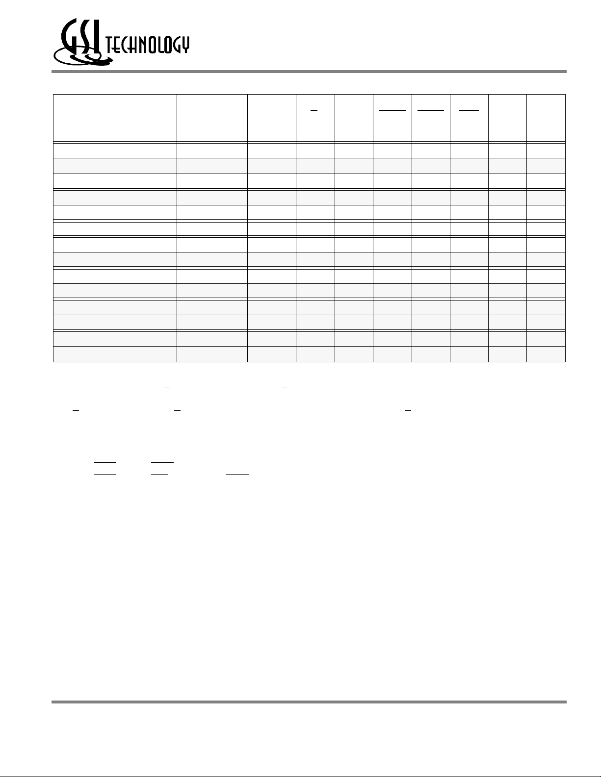
-150 -138 -133 -117 -100 -66
Pipeline
3-1-1-1
Flow
Through
2-1-1-1
tCycle
tKQ
IDD
tCycle
tKQ
IDD
6.6ns
3.8ns
270mA
10.5ns
9ns
170mA
7.25ns
4ns
245mA
15ns
9.7ns
120mA
7.5ns
4ns
240mA
15ns
10ns
120mA
8.5ns
4.5
210mA
15ns
11ns
120mA
10ns
5ns
180mA
15ns
12ns
120mA
12.5ns
6ns
150mA
20ns
18ns
95mA
Functional Description
Applications
The GS820E32 is a 2,097,152 bit high performance synchronous
SRAM with a 2 bit burst address counter. Although of a type originally
developed for Level 2 Cache applications supporting high
performance CPU’s, the device now finds application in synchronous
SRAM applications ranging from DSP main store to networking chip
set support.
Controls
Addresses, data I/O’s, chip enables (E1, E2, E3), address burst control
inputs (ADSP, ADSC, ADV) and write control inputs (Bx, BW, GW) are
synchronous and are controlled by a positive edge triggered clock
input (CK). Output enable (G) and power down control (ZZ) are
asynchronous inputs. Burst cycles can be initiated with either ADSP
or ADSC inputs. In Burst mode, subsequent burst addresses are
generated internally and are controlled by ADV. The burst address
counter may be configured to count in either linear or interleave order
with the Linear Burst Order (LBO) input. The Burst function need not
be used. New addresses can be loaded on every cycle with no
degradation of chip performance.
150Mhz - 66Mhz
9ns - 18ns
3.3V VDD
3.3V & 2.5V I/O
Flow Through / Pipeline Reads
The function of the Data Output register can be controlled by the user
via the FT mode pin/bump (Pin 14 in the TQFP, bump 1F in the FPBGA). Holding the FT mode pin/bump low, places the RAM in Flow
through mode, causing output data to bypass the Data Output
Register. Holding FT high places the RAM in Pipelined Mode,
activating the rising edge triggered Data Output Register.
DCD Pipelined Reads
The GS820E32 is a DCD (Dual Cycle Deselect) pipelined
synchronous SRAM. SCD (Single Cycle Deselect) versions are also
available. DCD SRAMs pipeline disable commands to the same
degree as read commands. DCD RAMs hold the deselect command
for one full cycle and then begin turning off their outputs just after the
second rising edge of clock.
Byte Write and Global Write
Byte write operation is performed by using byte write enable (BW)
input combined with one or more individual byte write signals (Bx). In
addition, Global Write (GW) is available for writing all bytes at one
time, regardless of the Byte Write control inputs.
Sleep Mode
Low power (Sleep mode) is attained through the assertion (High) of
the ZZ signal, or by stopping the clock (CK). Memory data is retained
during Sleep mode.
Core and Interface Voltages
The GS820E32 operates on a 3.3V power supply and all inputs/
outputs are 3.3V and 2.5V compatible. Separate output power (VDDQ)
pins are used to de-couple output noise from the internal circuit.
Rev: 1.03 2/2000 1/23 © 1999, Giga Semiconductor, Inc.
Specifications cited are subject to change without notice. For latest documentation see http://www.gsitechnology.com. D
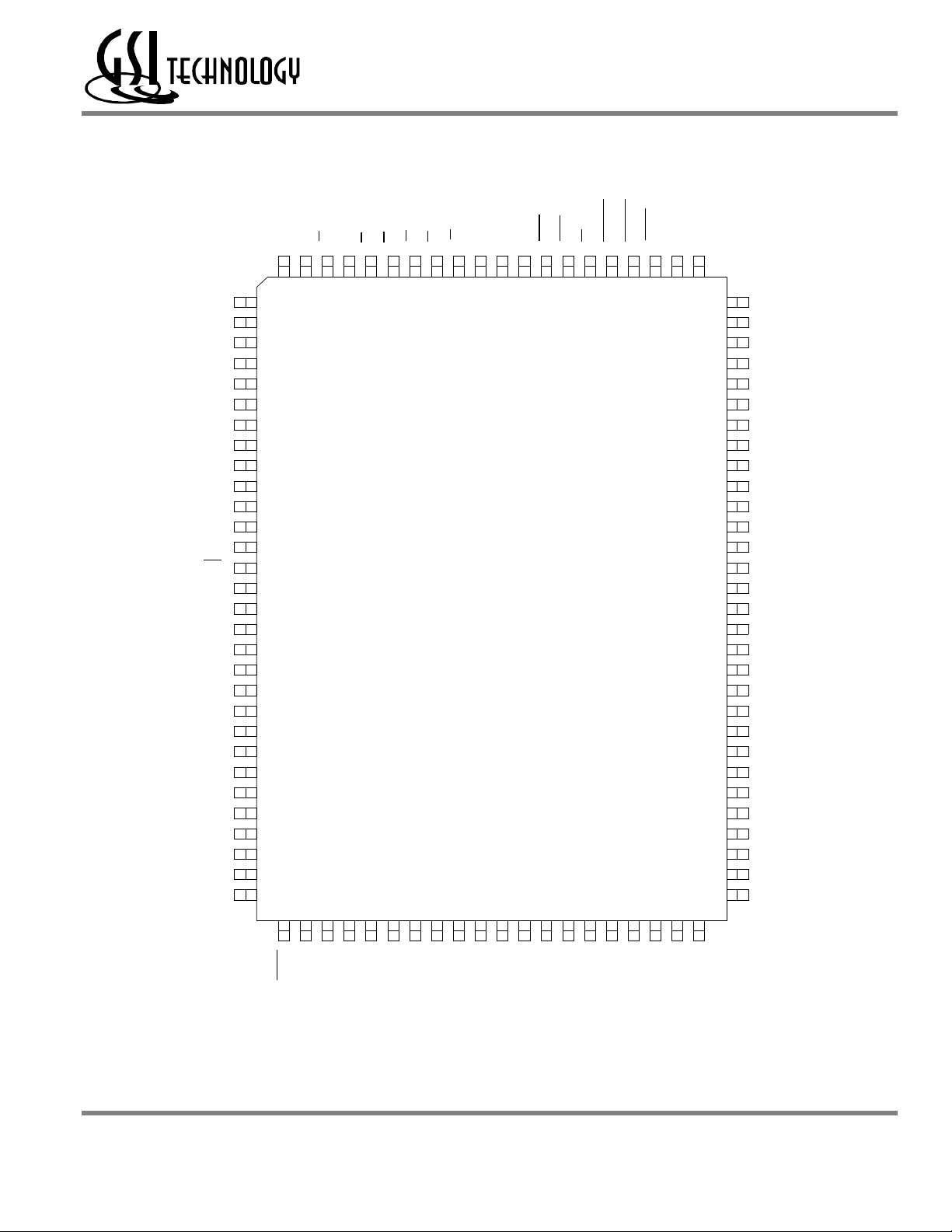
GS820E32 100 Pin TQFP and QFP Pinout
GS820E32T/Q-150/138/133/117/100/66
NC
DQC8
DQC7
VDDQ
VSS
DQC6
DQC5
DQC4
DQC3
VSS
VDDQ
DQC2
DQC1
FT
VDD
NC
VSS
DQD1
DQD2
VDDQ
VSS
DQD3
DQD4
DQD5
DQD6
VSS
VDDQ
DQD7
DQD8
NC
A6
E1
A7
E2
BC
BD
100 99 98 97 96 95 94 93 92 91 90 89 88 87 86 85 84 83 82 81
1
2
3
4
5
6
7
8
9
10
11
12
13
14
15
16
17
18
19
20
21
22
23
24
25
26
27
28
29
30
31 32 33 34 35 36 37 38 39 40 41 42 43 44 45 46 47 48 49 50
E3
BB
BA
64K x 32
Top View
VDD
VSS
BW
GW
CK
G
ADV
ADSP
ADSC
A8
A9
80
79
78
77
76
75
74
73
72
71
70
69
68
67
66
65
64
63
62
61
60
59
58
57
56
55
54
53
52
51
NC
DQB8
DQB7
VDDQ
VSS
DQB6
DQB5
DQB4
DQB3
VSS
VDDQ
DQB2
DQB1
VSS
NC
VDD
ZZ
DQA1
DQA2
VDDQ
VSS
DQA3
DQA4
DQA5
DQA6
VSS
VDDQ
DQA7
DQA8
NC
A5
A4
A3
A2
A1
A0
NC
LBO
NC
NC
VSS
VDD
A11
NC
A10
A12
A13
NC
A14
A15
Rev: 1.03 2/2000 2/23 © 1999, Giga Semiconductor, Inc.
Specifications cited are subject to change without notice. For latest documentation see http://www.gsitechnology.com. D
GS820E32T/Q-150/138/133/117/100/66
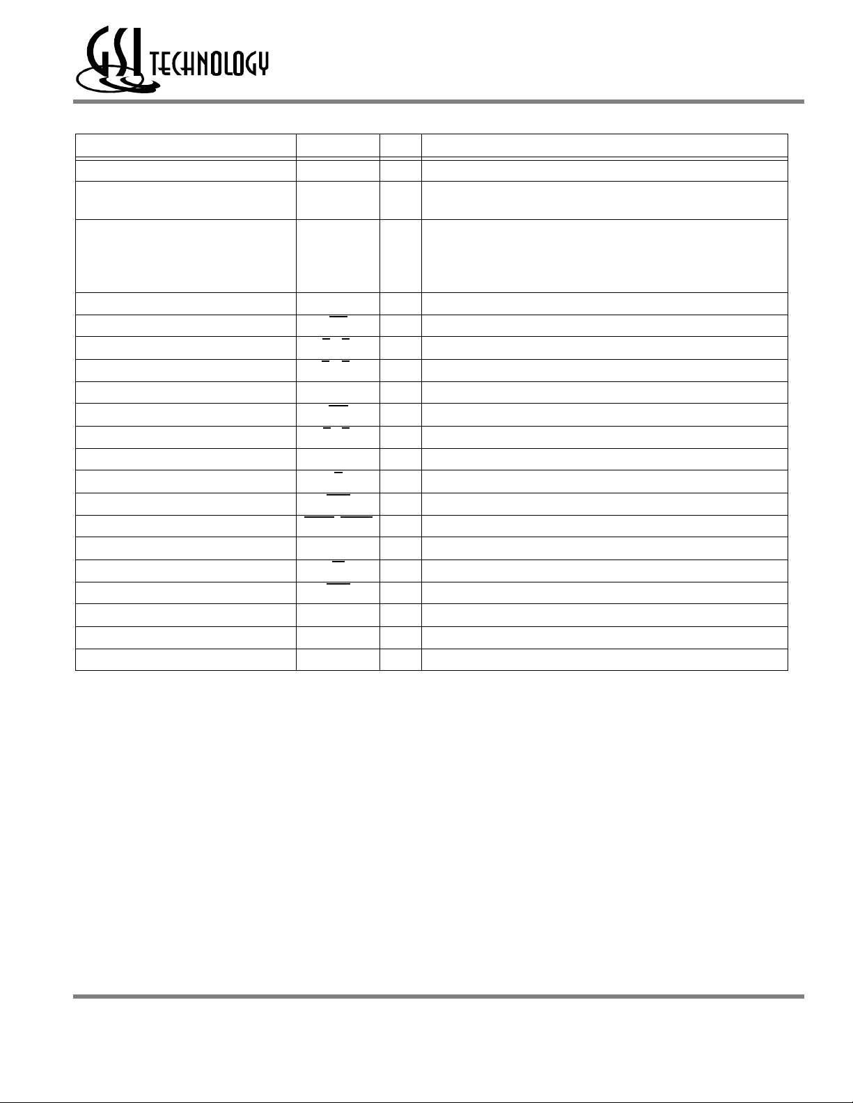
TQFP Pin Description
Pin Location Symbol Type Description
37, 36 A0, A1 I Address field LSB’s and Address Counter preset Inputs
35, 34, 33, 32, 100, 99, 82, 81, 44, 45,
46, 47, 48, 49
52, 53, 56, 57, 58, 59, 62, 63
68, 69, 72, 73, 74, 75, 78, 79
2, 3, 6, 7, 8, 9, 12, 13
18, 19, 22, 23, 24, 25, 28, 29
16, 38, 39, 42, 43, 66, 50, 51, 80, 1, 30 NC No Connect
87 BW I Byte Write. Writes all enabled bytes. Active Low.
93, 94 BA, BB I Byte Write Enable for DQA, DQB Data I/O’s. Active Low.
95, 96 BC, BD I Byte Write Enable for DQC, DQD Data I/O’s. Active Low.
89 CK I Clock Input Signal. Active High.
88 GW I Global Write Enable. Writes all bytes. Active Low.
98, 92 E1, E3 I Chip Enable. Active Low.
97 E2 I Chip Enable. Active High.
86 G I Output Enable. Active Low.
83 ADV I Burst address counter advance enable. Active Low.
84, 85 ADSP, ADSC I Address Strobe (Processor, Cache Controller). Active Low.
64 ZZ I Sleep Mode control. Active High.
14 FT I Flow Through or Pipeline mode. Active Low.
31 LBO I Linear Burst Order mode. Active Low.
15, 41, 65, 91 VDD I Core power supply.
5,10,17, 21, 26, 40, 55, 60, 67, 71, 76, 90 VSS I I/O and Core Ground.
4, 11, 20, 27, 54, 61, 70, 77 VDDQ I Output driver power supply.
A2-15 I Address Inputs
DQA1-DQA8
DQB1-DQB8
DQC1-DQC8
DQD1-DQD8
I/O Data Input and Output pins.
E
Rev: 1.03 2/2000 3/23 © 1999, Giga Semiconductor, Inc.
Specifications cited are subject to change without notice. For latest documentation see http://www.gsitechnology.com. D
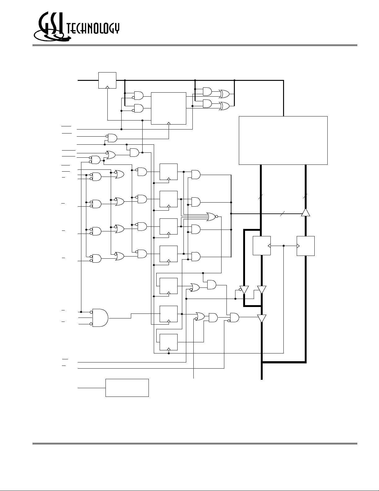
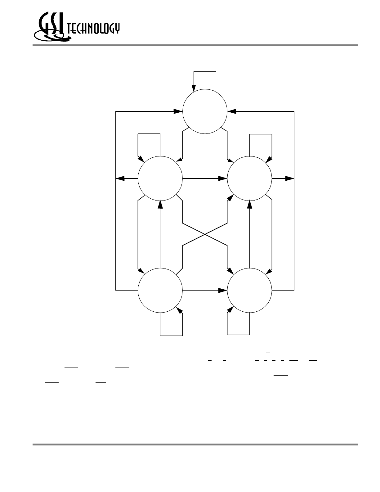
GS820E18/32/36 Block Diagram
A0-An
LBO
ADV
CK
ADSC
ADSP
GW
BW
BA
Register
D Q
A0
A1
D0
D1
Counter
Load
Register
D Q
Q0
Q1
GS820E32T/Q-150/138/133/117/100/66
A0
A1
A
Memory
Array
Q D
BB
BC
BD
E1
E2
E3
FT
G
Register
D Q
Register
D Q
Register
D Q
Register
D Q
Register
D Q
Register
D Q
32
4
DQ
Register
32
Register
DQ
ZZ
Power Down
Control
0
DQx1-DQx8
Rev: 1.03 2/2000 4/23 © 1999, Giga Semiconductor, Inc.
Specifications cited are subject to change without notice. For latest documentation see http://www.gsitechnology.com. D
GS820E32T/Q-150/138/133/117/100/66
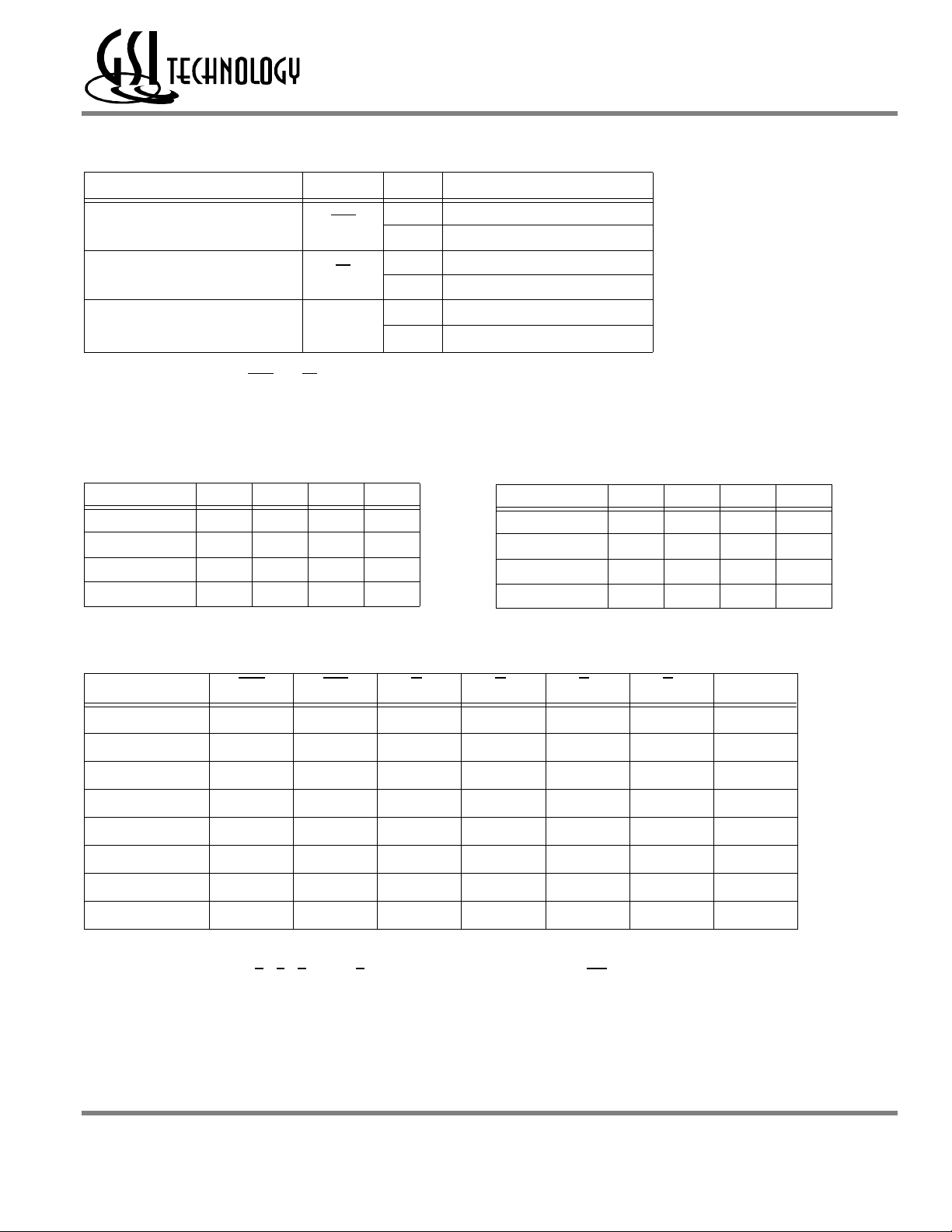
Linear Burst Sequence
I
Mode Pin Functions
Mode Name Pin Name State Function
Burst Order Control LBO
Output Register Control FT
Power Down Control ZZ
Note:
There are pull up devices on LBO and FT pins and a pull down device on and ZZ pin, so those input pins can be unconnected and the chip will
operate in the default states as specified in the above tables.
Burst Counter Sequences
A[1:0] A[1:0] A[1:0] A[1:0]
1st address 00 01 10 11
2nd address 01 10 11 00
3rd address 10 11 00 01
4th address 11 00 01 10
Note: The burst counter wraps to initial state on the 5th clock.
L Linear Burst
H or NC Interleaved Burst
L Flow Through
H or NC Pipeline
L or NC Active
H
Standby, IDD = I
nterleaved Burst Sequence
1st address 00 01 10 11
2nd address 01 00 11 10
3rd address 10 11 00 01
4th address 11 10 01 00
Note: The burst counter wraps to initial state on the 5th clock.
SB
A[1:0] A[1:0] A[1:0] A[1:0]
Byte Write Truth Table
Function GW BW BA BB BC BD Notes
Read H H X X X X 1
Read H L H H H H 1
Write byte A H L L H H H 2, 3
Write byte B H L H L H H 2, 3
Write byte C H L H H L H 2, 3, 4
Write byte D H L H H H L 2, 3, 4
Write all bytes H L L L L L 2, 3, 4
Write all bytes L X X X X X
Note:
1. All byte outputs are active in read cycles regardless of the state of Byte Write Enable inputs.
2. Byte Write Enable inputs BA, BB, BC and/or BD may be used in any combination with BW to write single or multiple bytes.
3. All byte I/O’s remain High-Z during all write operations regardless of the state of Byte Write Enable inputs.
Rev: 1.03 2/2000 5/23 © 1999, Giga Semiconductor, Inc.
Specifications cited are subject to change without notice. For latest documentation see http://www.gsitechnology.com. D
GS820E32T/Q-150/138/133/117/100/66
Synchronous Truth Table
State
Operation Address Used
Deselect Cycle, Power Down None X H X X L X X High-Z
Deselect Cycle, Power Down None X L F L X X X High-Z
Deselect Cycle, Power Down None X L F H L X X High-Z
Read Cycle, Begin Burst External R L T L X X X Q
Read Cycle, Begin Burst External R L T H L X F Q
Write Cycle, Begin Burst External W L T H L X T D
Read Cycle, Continue Burst Next CR X X H H L F Q
Read Cycle, Continue Burst Next CR H X X H L F Q
Write Cycle, Continue Burst Next CW X X H H L T D
Write Cycle, Continue Burst Next CW H X X H L T D
Read Cycle, Suspend Burst Current X X H H H F Q
Read Cycle, Suspend Burst Current H X X H H F Q
Write Cycle, Suspend Burst Current X X H H H T D
Write Cycle, Suspend Burst Current H X X H H T D
Note:
1. X = Don’t Care, H = High, L = Low.
2. E = T (True) if E2 = 1 and E3 = 0; E = F (False) if E2 = 0 or E3 = 1.
3. W = T (True) and F (False) is defined in the Byte Write Truth Table preceding.
4. G is an asynchronous input. G can be driven high at any time to disable active output drivers. G low can only enable active drivers (shown
as “Q” in the Truth Table above).
Diagram
5
Key
E1
2
E
ADSP ADSC ADV
W
3
DQ
4
5. All input combinations shown above are tested and supported. Input combinations shown in gray boxes need not be used to accomplish
basic synchronous or synchronous burst operations and may be avoided for simplicity.
6. Tying ADSP high and ADSC low allows simple non-burst synchronous operations. See BOLD items above.
7. Tying ADSP high and ADV low while using ADSC to load new addresses allows simple burst operations. See ITALIC items above.
Rev: 1.03 2/2000 6/23 © 1999, Giga Semiconductor, Inc.
Specifications cited are subject to change without notice. For latest documentation see http://www.gsitechnology.com. D
GS820E32T/Q-150/138/133/117/100/66
Simplified State Diagram
X
Deselect
W R
W
X
Simple Synchronous OperationSimple Burst Synchronous Operation
First Write
W R
Burst Write
CW CR
R
CR
R
CR
R
First Read
Burst Read
X
CRCW
XX
Notes:
1. The diagram shows only supported (tested) synchronous state transitions. The diagram presumes G is tied Low.
2. The upper portion of the diagram assumes active use of only the Enable (E1, E2, E3) and Write (BA, BB, BC, BD, BW and GW) control inputs
and that ADSP is tied high and ADSC is tied low.
3. The upper and lower portions of the diagram together assume active use of only the Enable, Write and ADSC control inputs and assumes
ADSP is tied high and ADV is tied low.
Rev: 1.03 2/2000 7/23 © 1999, Giga Semiconductor, Inc.
Specifications cited are subject to change without notice. For latest documentation see http://www.gsitechnology.com. D
 Loading...