

GSI GS8180D18D-333I, GS8180D18D-333, GS8180D18D-300I, GS8180D18D-300, GS8180D18D-250I Datasheet
...
Rev: 2.00f 6/2002 1/27 © 2002, Giga Semiconductor, Inc.
Specifications cited are design targets and are subject to change without notice. For latest documentation contact your GSI representative.
Preliminary
GS8180D18D-333/300/250/200
18Mb Σ2x2B4
SigmaQuad SRAM
200 MHz–333 MHz
1.8 V V
DD
1.8 V and 1.5 V I/O
165-Bump BGA
Commercial Temp
Industrial Temp
Features
• Simultaneous Read and Write SigmaQuad™ Interface
• JEDEC-standard pinout and package
• Dual Double Data Rate interface
• Echo Clock outputs track data output drivers
• Byte Write controls sampled at data-in time
• Burst of 4 Read and Write
• 1.8 V +150/–100 mV core power supply
• 1.5 V or 1.8 V HSTL Interface
• Pipelined read operation
• Fully coherent read and write pipelines
• ZQ mode pin for programmable output drive strength
• IEEE 1149.1 JTAG-compliant Boundary Scan
• 165-bump, 13 mm x 15 mm, 1 mm bump pitch BGA package
• Pin-compatible with future 36Mb, 72Mb, and 144Mb devices
SigmaRAM™ Family Overview
GS8180D18 are built in compliance with the SigmaQuad SRAM
pinout standard for Separate I/O synchronous SRAMs. They are
18,874,368-bit (18Mb) SRAMs. These are the first in a family of wide,
very low voltage HSTL I/O SRAMs designed to operate at the speeds
needed to implement economical high performance networking
systems.
SigmaQuad SRAMs are offered in a number of configurations. Some
emulate and enhance other synchronous separate I/O SRAMs. A
higher performance SDR (Single Data Rate) Burst of 2 version is also
offered. The logical differences between the protocols employed by
these RAMs hinge mainly on various combinations of address
bursting, output data registering, and write cueing. Along with the
Common I/O family of SigmaRAMs, the SigmaQuad family of SRAMs
allows a user to implement the interface protocol best suited to the
task at hand.
Clocking and Addressing Schemes
A
Σ
2x2B4 SigmaQuad SRAM is a synchronous device. It employs
two input register clock inputs, K and K
. K and K are independent
single-ended clock inputs, not differential inputs to a single differential
clock input buffer. The device also allows the user to manipulate the
output register clock inputs quasi independently with the C and C
clock inputs. C and C
are also independent single-ended clock inputs,
not differential inputs. If the C clocks are tied high, the K clocks are
routed internally to fire the output registers instead. Each
Σ
2x2B4
SigmaQuad SRAM also supplies Echo Clock outputs, CQ and CQ
,
that are synchronized with read data output. When used in a source
synchronous clocking scheme, these Echo Clock outputs can be used
to fire input registers at the data’s destination.
Because Separate I/O
Σ
2x2B4 RAMs always transfer data in four
packets, A0 and A1 are internally set to 0 for the first read or write
transfer, and automatically incremented by 1 for the next transfers.
Because the LSBs are tied off internally, the address field of a
Σ
2x2B4 RAM is always two address pins less than the advertised
index depth (e.g., the 1M x 18 has a 256K addressable index).
- 333 -300 -250 -200
tKHKH 3.0 ns 3.3 ns 4 ns 5 ns
tKHQV 1.6 ns 1.8 ns 2.1 ns 2.3 ns
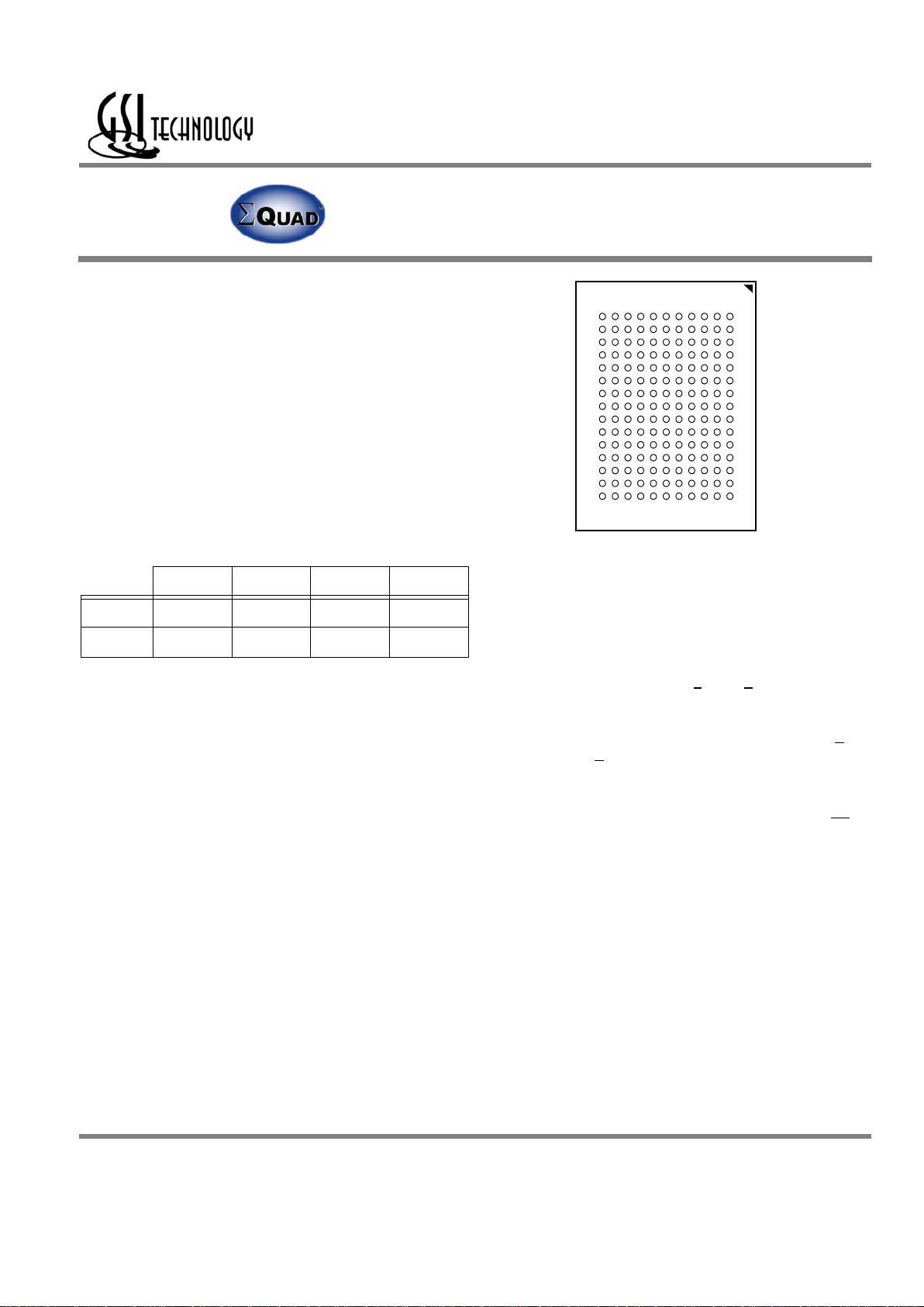
165-Bump, 13 mm x 15 mm BGA
1 mm Bump Pitch, 11 x 15 Bump Array
Bottom View
JEDEC Std. MO-216, Variation CAB-1
Rev: 2.00f 6/2002 2/27 © 2002, Giga Semiconductor, Inc.
Specifications cited are design targets and are subject to change without notice. For latest documentation contact your GSI representative.
Preliminary
GS8180D18D-333/300/250/200
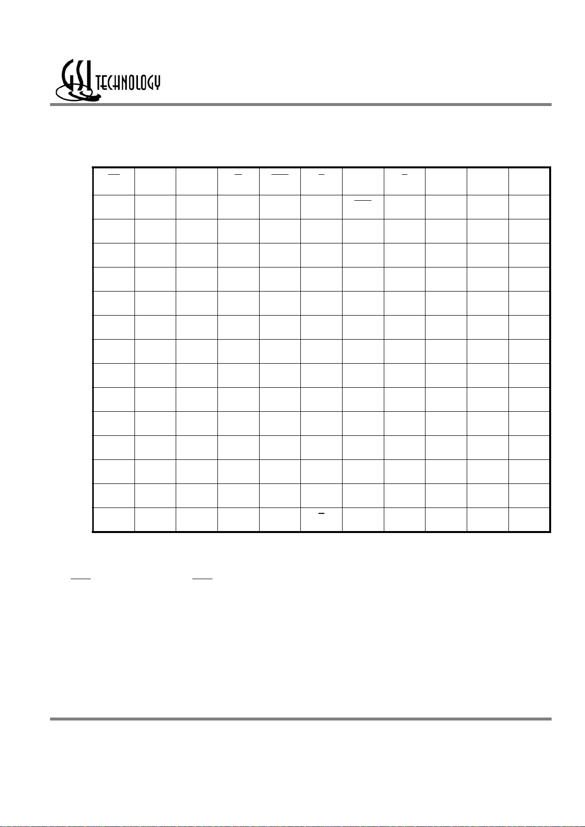
1M x 18 SigmaQuad SRAM — Top View
1234567891011
A CQ
MCL/SA
(144Mb)
NC/SA
(36Mb)
W
BW1 K NC R SA
MCL/SA
(72Mb)
CQ
B NC Q9 D9 SA NC K BW0
SA NC NC Q8
C NC NC D10 V
SS
SA
NC SA V
SS
NC Q7 D8
D NC D11 Q10 V
SS
V
SS
V
SS
V
SS
V
SS
NC NC D7
E NC NC Q11 V
DDQ
V
SS
V
SS
V
SS
V
DDQ
NC D6 Q6
F NC Q12 D12 V
DDQ
V
DD
V
SS
V
DD
V
DDQ
NC NC Q5
G NC D13 Q13 V
DDQ
V
DD
V
SS
V
DD
V
DDQ
NC NC D5
H NC V
REF
V
DDQ
V
DDQ
V
DD
V
SS
V
DD
V
DDQ
V
DDQ
V
REF
ZQ
J NC NC D14 V
DDQ
V
DD
V
SS
V
DD
V
DDQ
NC Q4 D4
K NC NC Q14 V
DDQ
V
DD
V
SS
V
DD
V
DDQ
NC D3 Q3
L NC Q15 D15 V
DDQ
V
SS
V
SS
V
SS
V
DDQ
NC NC Q2
M NC NC D16 V
SS
V
SS
V
SS
V
SS
V
SS
NC Q1 D2
N NC D17 Q16 V
SS
SA SA SA V
SS
NC NC D1
P NC NC Q17 SA SA C SA SA NC D0 Q0
R TDO TCK SA SA SA C
SA SA SA TMS TDI
11 x 15 Bump BGA—13 x 15 mm2 Body—1 mm Bump Pitch
Notes:
1. Expansion addresses: A3 for 36Mb, A10 for 72Mb, A2 for 144Mb
2. BW0
controls writes to D0:D8. BW1 controls writes to D9:D17.
3. MCL = Must Connect Low
4. It is recommended that H1 be tied low for compatibility with future devices.
Rev: 2.00f 6/2002 3/27 © 2002, Giga Semiconductor, Inc.
Specifications cited are design targets and are subject to change without notice. For latest documentation contact your GSI representative.
Preliminary
GS8180D18D-333/300/250/200
Note: NC = Not Connected to die or any other pin
Background
Separate I/O SRAMs, from a system architecture point of view, are attractive in applications where alternating reads and writes are needed.
Therefore, the SigmaQuad SRAM interface and truth table are optimized for alternating reads and writes. Separate I/O SRAMs are unpopular in
applications where multiple reads or multiple writes are needed because burst read or write transfers from Separate I/O SRAMs can cut the
RAM’s bandwidth in half.
A SigmaQuad SRAM can begin an alternating sequence of reads and writes with either a read or a write. In order for any separate I/O SRAM that
shares a common address between its two ports to keep both ports running all the time, the RAM must implement some sort of burst transfer
protocol. The burst must be at least long enough to cover the time the opposite port is receiving instructions on what to do next. The rate at which
a RAM can accept a new random address is the most fundamental performance metric for the RAM. Each of the three SigmaQuad SRAMs
support similar address rates because random address rate is determined by the internal performance of the RAM and they are all based on the
Pin Description Table
Symbol Description Type Comments
SA Synchronous Address Inputs Input —
NC No Connect — —
R
Synchronous Read Input Active Low
W
Synchronous Write Input Active Low
BW0
–BW1 Synchronous Byte Writes Input
Active Low
K Input Clock Input Active High
K
Input Clock Input Active Low
C Output Clock Input Active High
C
Output Clock Input Active Low
TMS Test Mode Select Input —
TDI Test Data Input Input —
TCK Test Clock Input Input —
TDO Test Data Output Output —
V
REF
HSTL Input Reference Voltage Input —
ZQ Output Impedance Matching Input Input —
MCL Must Connect Low — —
CQ Synchronous Echo Clock Output Output Echoes C or K Clock
CQ
Synchronous Echo Clock-bar Output Output Echoes C or K Clock
D0–D17 Synchronous Data Inputs Input —
Q0–Q17 Synchronous Data Outputs Output —
V
DD
Power Supply Supply 2.5 V Nominal
V
DDQ
Isolated Output Buffer Supply Supply 1.5 V Nominal
V
SS
Power Supply: Ground Supply —

Rev: 2.00f 6/2002 4/27 © 2002, Giga Semiconductor, Inc.
Specifications cited are design targets and are subject to change without notice. For latest documentation contact your GSI representative.
Preliminary
GS8180D18D-333/300/250/200
same internal circuits. Differences between the truth tables of the different SigmaQuad SRAMs, or any other Separate I/O SRAMs, follow from
differences in how the RAM’s interface is contrived to interact with the rest of the system. Each mode of operation has its own advantages and
disadvantages. The user should consider the nature of the work to be done by the RAM to evaluate which version is best suited to the application
at hand.
Alternating Read-Write Operations
SigmaQuad SRAMs follow a few simple rules of operation.
- Read or Write commands issued on one port are never allowed to interrupt an operation in progress on the other port.
- Read or Write data transfers in progress may not be interrupted and re-started.
- R
and W high always deselects the RAM but does not disable the CQ or CQ output pins.
- All address, data, and control inputs are sampled on clock edges.
In order to enforce these rules, each RAM combines present state information with command inputs. See the Truth Table for details.
Rev: 2.00f 6/2002 5/27 © 2002, Giga Semiconductor, Inc.
Specifications cited are design targets and are subject to change without notice. For latest documentation contact your GSI representative.
Preliminary
GS8180D18D-333/300/250/200
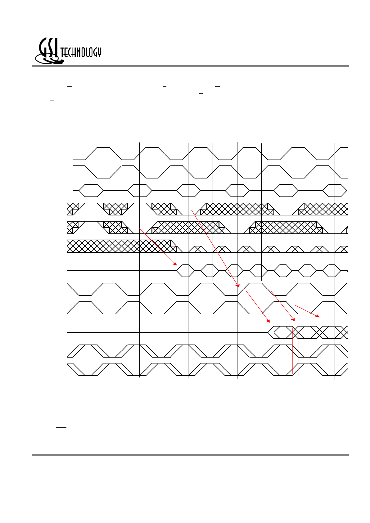
Σ
2x2B4 SigmaQuad SRAM DDR Read
The status of the Address Input, W
, and R pins are sampled at each rising edge of K. W and R high causes chip disable. A low on the Read
Enable-bar pin, R
, begins a read cycle. R is always ignored if the previous command loaded was a read command. The four resulting data output
transfers begin after the next rising edge of the K clock. Data is clocked out by the next rising edge of the C, the rising edge of C
after that, the
next rising edge of C, and finally by the next rising edge of C
.
Σ
2x2B4 Double Data Rate SigmaQuad SRAM Read First
Dwg Re v. G
DC0 DC1 DC2 DC3 DE0
QB0 QB1 QB2 QB3 QD0
/CQ
/W
D
Q
CQ
/BWx
C
/C
DE F
/R
Address XX B C
Write Read Write Read
K
/K
No Op Read
Rev: 2.00f 6/2002 6/27 © 2002, Giga Semiconductor, Inc.
Specifications cited are design targets and are subject to change without notice. For latest documentation contact your GSI representative.
Preliminary
GS8180D18D-333/300/250/200
Σ
2x2B4 SigmaQuad SRAM DDR Write
The status of the Address Input, W
, and R pins are sampled at each rising edge of K. W and R high causes chip disable. A low on the Write
Enable-bar pin, W
, and a high on the Read Enable-bar pin, R, begins a write cycle. W is always ignored if the previous command was a write
command. Data is clocked in by the next rising edge of K, the rising edge of K
after that, the next rising edge of K, and finally by the next rising
edge of K
.
Σ
2x2B4 Double Data Rate SigmaQuad SRAM Write First
Special Functions
Byte Write Control
Byte Write Enable pins are sampled at the same time that Data In is sampled. A high on the Byte Write Enable pin associated with a particular
byte (e.g., BW0
controls D0–D8 inputs) will inhibit the storage of that particular byte, leaving whatever data may be stored at the current address
at that byte location undisturbed. Any or all of the Byte Write Enable pins may be driven high or low during the data in sample times in a write
sequence.
Dwg Re v. G
DB0 DB1 DB2 DB3 DD0 DD1 DD2
QC0 QC1 QC2
CQ
/CQ
DE
/W
D
Q
C
/C
/BWx
F
/R
Address XX B C
Read Write Read Write
K
/K
No O p Write

Rev: 2.00f 6/2002 7/27 © 2002, Giga Semiconductor, Inc.
Specifications cited are design targets and are subject to change without notice. For latest documentation contact your GSI representative.
Preliminary
GS8180D18D-333/300/250/200
Each write enable command and write address loaded into the RAM provides the base address for a 4 beat data transfer. The x18 version of the
RAM, for example, may write 72 bits in association with each address loaded. Any 9-bit byte may be masked in any write sequence.
Example x18 RAM Write Sequence using Byte Write Enables
Resulting Write Operation
Output Register Control
SigmaQuad SRAMs offer two mechanisms for controlling the output data registers. Typically, control is handled by the Output Register Clock
inputs, C and C
. The Output Register Clock inputs can be used to make small phase adjustments in the firing of the output registers by allowing
the user to delay driving data out as much as a few nanoseconds beyond the next rising edges of the K and K
clocks. If the C and C clock inputs
are tied high, the RAM reverts to K and K
control of the outputs, allowing the RAM to function as a conventional pipelined read SRAM.
Echo Clock
SigmaQuad SRAMs feature Echo Clock outputs, CQ and CQ
, that track the performance of the output drivers. The Echo Clocks are delayed
copies of the Output Register clocks, C and C
or K and K (if the C and C clock inputs are tied high). Echo Clocks are designed to track changes
in output driver delays due to variance in die temperature and supply voltage. The Echo Clocks are designed to fire with the rest of the data
output drivers. SigmaQuad SRAMs provide both in-phase, or true, Echo Clock output, CQ and inverted Echo Clock output CQ
.
Echo Clocks are always active.
Neither inhibiting reads via holding R
high, nor deselection of the RAM via holding R and W high will
deactivate the Echo Clocks.
Data In Sample
Time
BW0 BW1 D0–D8 D9–D17
Beat 1 0 1 Data In Don’t Care
Beat 2 1 0 Don’t Care Data In
Beat 3 0 0 Data In Data In
Beat 4 1 0 Don’t Care Data In
Byte 1
D0–D8
Byte 2
D9–D17
Byte 3
D0–D8
Byte 4
D9–D17
Byte 5
D0–D8
Byte 6
D9–D17
Byte 7
D0–D8
Byte 8
D9–D17
Written Unchanged Unchanged Written Written Written Unchanged Written
Rev: 2.00f 6/2002 8/27 © 2002, Giga Semiconductor, Inc.
Specifications cited are design targets and are subject to change without notice. For latest documentation contact your GSI representative.
Preliminary
GS8180D18D-333/300/250/200
Example Four Bank Depth Expansion Schematic
A
K
R
W
A0–A
n
K
W
0
D1–D
n
Bank 0
Bank 1 Bank 2
Bank 3
R
0
CQ
D
A
K
W
CQ
D
A
K
W
CQ
D
A
K
W
CQ
D
R
R
R
QQQ Q
CC CC
Q1–Q
n
C
CQ
0
CQ
1
CQ
2
CQ
3
W
1
R
1
W
2
R
2
W
3
R
3
Note: For simplicity BWn, K, C and CQ are not shown.
Rev: 2.00f 6/2002 9/27 © 2002, Giga Semiconductor, Inc.
Specifications cited are design targets and are subject to change without notice. For latest documentation contact your GSI representative.
Preliminary
GS8180D18D-333/300/250/200
Σ
2x2B4 SigmaQuad SRAM Depth Expansion
Dwg Re v. G
DC0 DC1 DC2 DC3 DE0 DE1 DE2 DE3
QD0 QD1 QD2 QD3
QB0 QB1 QB2 QB3
QB0 QB1 QB2 QB3 QD0 QD1 QD2 QD3
CQ
Bank 1
C
Q
Bank 2
Q
Bank 1
B
/C
CQ
Bank 2
Q Bank 1 +
Q Bank 2
/R2
/R1
/W1
/W2
D
Bank 1
D
Bank 2
GDEFCAddress XX
Wri t e
- Bank 2 Bank 2 Bank 1 Bank 2 Bank 1 Bank 1
Write Read Write Read
K
/K
No Op Read

Rev: 2.00f 6/2002 10/27 © 2002, Giga Semiconductor, Inc.
Specifications cited are design targets and are subject to change without notice. For latest documentation contact your GSI representative.
Preliminary
GS8180D18D-333/300/250/200
FLXDrive-II Output Driver Impedance Control
HSTL I/O SigmaQuad SRAMs are supplied with programmable impedance output drivers. The ZQ pin must be connected to V
SS
via an external
resistor, RQ, to allow the SRAM to monitor and adjust its output driver impedance. The value of RQ must be 5X the value of the intended line
impedance driven by the SRAM. The allowable range of RQ to guarantee impedance matching with a vendor-specified tolerance is between
150Ω and 300Ω. Periodic readjustment of the output driver impedance is necessary as the impedance is affected by drifts in supply voltage and
temperature. A clock cycle counter periodically triggers an impedance evaluation, resets and counts again. Each impedance evaluation may
move the output driver impedance level one step at a time towards the optimum level. The output driver is implemented with discrete binary
weighted impedance steps. Impedance updates for “0s” occur whenever the SRAM is driving “1s” for the same DQs (and vice-versa for “1s”) or
the SRAM is in HI-Z. The SRAM requires 32K start-up cycles, selected or deselected, after V
DD
reaches its operating range to reach its
programmed output driver impedance.
Separate I/O Σ2x2B4 SigmaQuad SRAM Truth Table
ARW
Previous
Operation
Current
Operation
DDDDQQQQ
K
↑
(tn)
K
↑
(tn)
K
↑
(tn)
K
↑
(t
n-1
)
K
↑
(tn)
K
↑
(t
n+1
)
K
↑
(t
n+1½
)
K
↑
(t
n+2
)
K
↑
(t
n+2½
)
K
↑
(t
n+1
)
K
↑
(t
n+1½
)
K
↑
(t
n+2
)
K
↑
(t
n+2½
)
X 1 1 Deselect Deselect X X — — Hi-Z Hi-Z — —
X 1 X Write Deselect D2 D3 — — Hi-Z Hi-Z — —
X X 1 Read Deselect X X — — Q2 Q3 — —
V 1 0 Deselect Write D0 D1 D2 D3 Hi-Z Hi-Z — —
V 0 X Deselect Read X X — — Q0 Q1 Q2 Q3
VX0 Read Write D0D1D2D3 Q2Q3 — —
V 0 X Write Read D2 D3 — — Q0 Q1 Q2 Q3
Notes:
1. “1” = input “high”; “0” = input “low”; “V” = input “valid”; “X” = input “don’t care”
2. “—” indicates that the input requirement or output state is determined by the next operation.
3. Q0, Q1, Q2, and Q3 indicate the first, second, third, and fourth pieces of output data transferred during Read operations.
4. D0, D1, D2, and D3 indicate the first, second, third, and fourth pieces of input data transferred during Write operations.
5. Qs are tristated for one cycle in response to Deselect and Write commands, one cycle after the command is sampled, except
when preceded by a Read command.
6. CQs are never tristated.
7. Users should not clock in metastable addresses.

Rev: 2.00f 6/2002 11/27 © 2002, Giga Semiconductor, Inc.
Specifications cited are design targets and are subject to change without notice. For latest documentation contact your GSI representative.
Preliminary
GS8180D18D-333/300/250/200
Byte Write Clock Truth Table
x18 Byte Write Enable (BWn) Truth Table
BW BW BW BW Current Operation D D D D
K
↑
(t
n+1
)
K
↑
(t
n+1½
)
K
↑
(t
n+2
)
K
↑
(t
n+2½
)
K
↑
(tn)
K
↑
(t
n+1
)
K
↑
(t
n+1½
)
K
↑
(t
n+2
)
K
↑
(t
n+2½
)
TTTT
Write
Dx stored if BWn
= 0 in all four data transfers
D0 D2 D3 D4
TFFF
Write
Dx stored if BWn
= 0 in 1st data transfer only
D0XXX
FTFF
Write
Dx stored if BWn
= 0 in 2nd data transfer only
XD1X X
FFTF
Write
Dx stored if BWn
= 0 in 3rd data transfer only
XXD2X
FFFT
Write
Dx stored if BWn
= 0 in 4th data transfer only
XXXD3
FFFF
Write Abort
No Dx stored in any of the four data transfers
XXXX
Notes:
1. “1” = input “high”; “0” = input “low”; “X” = input “don’t care”; “T” = input “true”; “F” = input “false”.
2. If one or more BWn
= 0, then BW = “T”, else BW = “F”.
BW0 BW1 D0–D8 D9–D17
1 1 Don’t Care Don’t Care
0 1 Data In Don’t Care
1 0 Don’t Care Data In
0 0 Data In Data In
Rev: 2.00f 6/2002 12/27 © 2002, Giga Semiconductor, Inc.
Specifications cited are design targets and are subject to change without notice. For latest documentation contact your GSI representative.
Preliminary
GS8180D18D-333/300/250/200
Recommended Operating Conditions
Absolute Maximum Ratings
(All voltages reference to V
SS
)
Symbol Description Value Unit
V
DD
Voltage on VDD Pins
–0.5 to 2.5 V
V
DDQ
Voltage in V
DDQ
Pins –0.5 to V
DD
V
V
REF
Voltage in V
REF
Pins –0.5 to V
DDQ
V
V
I/O
Voltage on I/O Pins
–0.5 to V
DDQ
+0.5 (≤ 2.5 V max.)
V
V
IN
Voltage on Other Input Pins
–0.5 to V
DDQ
+0.5 (≤ 2.5 V max.)
V
I
IN
Input Current on Any Pin +/–100 mA dc
I
OUT
Output Current on Any I/O Pin +/–100 mA dc
T
J
Maximum Junction Temperature 125
o
C
T
STG
Storage Temperature –55 to 125
o
C
Note:
Permanent damage to the device may occur if the Absolute Maximum Ratings are exceeded. Operation should be restricted to Recommended
Operating Conditions. Exposure to conditions exceeding the Recommended Operating Conditions, for an extended period of time, may affect
reliability of this component.
Power Supplies
Parameter Symbol Min. Typ. Max. Unit Notes
Supply Voltage
V
DD
1.7 1.8 1.95 V
1.8 V I/O Supply Voltage
V
DDQ
1.7 1.8 V 1
1.5 V I/O Supply Voltage
V
DDQ
1.4 1.5 1.6 V 1
Ambient Temperature
(Commercial Range Versions)
T
A
02570°C2
Ambient Temperature
(Industrial Range Versions)
T
A
–40 25 85 °C2
Notes:
1. Unless otherwise noted, all performance specifications quoted are evaluated for worst case at both 1.4 V ≤ V
DDQ
≤ 1.6 V (i.e., 1.5 V I/O)
and 1.7 V ≤ V
DDQ
≤ 1.95 V (i.e., 1.8 V I/O) and quoted at whichever condition is worst case.
2. The power supplies need to be powered up simultaneously or in the following sequence: V
DD
,
V
DDQ
, V
REF
, followed by signal inputs. The
power down sequence must be the reverse. V
DDQ
must not exceed VDD.
3. Most speed grades and configurations of this device are offered in both Commercial and Industrial Temperature ranges. The part number
of Industrial Temperature Range versions end the character “I”. Unless otherwise noted, all performance specifications quoted are
evaluated for worst case in the temperature range marked on the device.

Rev: 2.00f 6/2002 13/27 © 2002, Giga Semiconductor, Inc.
Specifications cited are design targets and are subject to change without notice. For latest documentation contact your GSI representative.
Preliminary
GS8180D18D-333/300/250/200
HSTL I/O AC Input Definitions
HSTL I/O DC Input Characteristics
Parameter Symbol Min Max Units Notes
DC Input Logic High
V
IH
(dc) V
REF
+ 200
mV 1
DC Input Logic Low
V
IL
(dc) V
REF
– 200
mV 1
V
REF
DC Voltage V
REF
(dc) V
DDQ
(min)/2 V
DDQ
(max)/2
V1
Notes:
1. Compatible with both 1.8 V and 1.5 V I/O drivers
HSTL I/O AC Input Characteristics
Parameter Symbol Min Max Units Notes
AC Input Logic High
V
IH
(ac) V
REF
+ 400
mV 3,4
AC Input Logic Low
V
IL
(ac) V
REF
– 400
mV 3,4
V
REF
Peak to Peak AC Voltage V
REF
(ac) 5% V
REF
(DC)
mV 1
Notes:
1. The peak to peak AC component superimposed on V
REF
may not exceed 5% of the DC component of V
REF
.
2. To guarantee AC characteristics, V
IH,VIL
, Trise, and Tfall of inputs and clocks must be within 10% of each other.
3. For devices supplied with HSTL I/O input buffers. Compatible with both 1.8 V and 1.5 V I/O drivers.
4. See AC Input Definition drawing below.
VIH (ac)
V
REF
VIL (ac)

Rev: 2.00f 6/2002 14/27 © 2002, Giga Semiconductor, Inc.
Specifications cited are design targets and are subject to change without notice. For latest documentation contact your GSI representative.
Preliminary
GS8180D18D-333/300/250/200
Capacitance
(T
A
= 25oC, f = 1 MHZ, V
DD
= 3.3 V)
Parameter Symbol Test conditions Typ. Max. Unit
Input Capacitance
C
IN
V
IN
= 0 V
45pF
Output Capacitance
C
OUT
V
OUT
= 0 V
67pF
Note: This parameter is sample tested.
Package Thermal Characteristics
Rating Layer Board Symbol Max Unit Notes
Junction to Ambient (at 200 lfm) single
R
ΘJA
TBD °C/W 1,2
Junction to Ambient (at 200 lfm) four
R
ΘJA
TBD °C/W 1,2
Junction to Case (TOP) —
R
ΘJC
TBD °C/W 3
Notes:
1. Junction temperature is a function of SRAM power dissipation, package thermal resistance, mounting board temperature,
ambient. Temperature air flow, board density, and PCB thermal resistance.
2. SCMI G-38-87
3. Average thermal resistance between die and top surface, MIL SPEC-883, Method 1012.1
AC Test Conditions
Parameter Conditions
Input high level
V
DDQ
Input low level 0 V
Max. input slew rate 2 V/ns
Input reference level
V
DDQ
/2
Output reference level
V
DDQ
/2
Notes: Test conditions as specified with output loading as shown unless otherwise noted.
20% tKHKH
V
SS
– 1.0 V
50%
V
SS
V
IH
Undershoot Measurement and Timing Overshoot Measurement and Timing
20% tKHKH
V
DD
+ 1.0 V
50%
V
DD
V
IL

Rev: 2.00f 6/2002 15/27 © 2002, Giga Semiconductor, Inc.
Specifications cited are design targets and are subject to change without notice. For latest documentation contact your GSI representative.
Preliminary
GS8180D18D-333/300/250/200
AC Test Load Diagram
Input and Output Leakage Characteristics
Parameter Symbol Test Conditions Min. Max Notes
Input Leakage Current
(except mode pins)
I
IL
V
IN
= 0 to V
DD
–2 uA 2 uA
Mode Pin Input Current
I
INM
V
DD ≥
V
IN
≥
VIL
0 V
≤ V
IN
≤ V
IL
–100 uA
–2 uA
2 uA
2 uA
Output Leakage Current
I
OL
Output Disable,
V
OUT
= 0 to V
DDQ
–2 uA 2 uA
Programmable Impedance HSTL Output Driver DC Electrical Characteristics
Parameter Symbol Min. Max. Units Notes
Output High Voltage
V
OH
V
DDQ / 2
V
DDQ
V 1,3
Output Low Voltage
V
OL
Vss
V
DDQ / 2
V 2,3
Notes:
1. I
OH
= (V
DDQ
/2) / (RQ/5) +/– 15% @ VOH = V
DDQ
/2 (for: 150Ω ≤ RQ ≤ 300Ω).
2. I
OL
= (V
DDQ
/2) / (RQ/5) +/– 15% @ VOL = V
DDQ
/2 (for: 150Ω ≤ RQ ≤ 300Ω).
3. Parameter tested with RQ = 250Ω and V
DDQ
= 1.5 V or 1.8 V
DQ
VT = V
DDQ
/2
50Ω
RQ = 250 Ω (HSTL I/O)

Rev: 2.00f 6/2002 16/27 © 2002, Giga Semiconductor, Inc.
Specifications cited are design targets and are subject to change without notice. For latest documentation contact your GSI representative.
Preliminary
GS8180D18D-333/300/250/200
Operating Currents
Parameter Org Symbol
-333 -300 -250
Test Conditions
0°C to
70°C
–40°C to
+85°C
0°C to
70°C
–40°C to
+85°C
0°C to
70°C
–40°C to
+85°C
Operating
Current
x18
IDD 400 mA TBD mA 375 mA TBD mA 330 mA TBD mA
R
and W ≤ V
IL
Max.
tKHKH ≥ tKHKH Min.
All other inputs
V
IN
≤ V
IL
Max. or V
IN
≥ V
IH
Min.
IDDQ 95 mA TBD mA 85 mA TBD mA 70 mA TBD mA
Chip Disable
Current
x18
ISB1 155 mA TBD mA 150 mA TBD mA 140 mA TBD mA
R
and W ≥ V
IH
Min.
tKHKH ≥ tKHKH Min.
All other inputs
V
IN
≤ V
IL
Max. or V
IN
≥ V
IH
Min.
ISBQ1 5 mA TBD mA 5 mA TBD mA 5 mA TBD mA
Note: Power measured with output pins floating.

Rev: 2.00f 6/2002 17/27 © 2002, Giga Semiconductor, Inc.
Specifications cited are design targets and are subject to change without notice. For latest documentation contact your GSI representative.
Preliminary
GS8180D18D-333/300/250/200
AC Electrical Characteristics
Parameter Symbol
-333 -300 -250 -200
Units Notes
Min Max Min Max Min Max Min Max
K, K Clock Cycle Time
C, C
Clock Cycle Time
t
KHKH
t
CHCH
3.0 — 3.3 — 4.0 — 5.0 — ns
K, K
Clock High Pulse Width
C, C
Clock High Pulse Width
t
KHKL
t
CHCL
1.2 — 1.3 — 1.5 — 2.0 — ns
K, K
Clock Low Pulse Width
C, C Clock Low Pulse Width
t
KLKH
t
CLCH
1.2 — 1.3 — 1.5 — 2.0 — ns
K Clock High to K
Clock High
C Clock High to C
Clock High
t
KHKH
t
CHCH
1.3 — 1.5 — 1.8 2.2 ns 4
K
Clock High to K Clock High
C Clock High to C Clock High
t
KHKH
t
CHCH
1.3 — 1.5 — 1.8 2.2 ns
K, K
Clock High to C, C Clock High
t
KHCH
0 1.3 0 1.45 0 1.8 0 2.3 ns
Address Input Setup Time
t
AVKH
0.4 — 0.4 — 0.5 — 0.6 — ns
Address Input Hold Time
t
KHAX
0.4 — 0.4 — 0.5 — 0.6 — ns
Control Input Setup Time
t
BVKH
0.4 — 0.4 — 0.5 — 0.6 — ns 1
Control Input Hold Time
t
KHBX
0.4 — 0.4 — 0.5 — 0.6 — ns 1
Data and Byte Write Input Setup Time
t
DVKH
0.3 — 0.3 — 0.35 — 0.4 — ns
Data and Byte Write Input Hold Time
t
KHDX
0.3 — 0.3 — 0.35 — 0.4 — ns
K, K
Clock High to Data Output Valid
C, C
Clock High to Data Output Valid
t
KHQV
t
CHQV
— 1.6 — 1.8 — 2.1 — 2.3 ns
K, K
Clock High to Data Output Hold
C, C
Clock High to Data Output Hold
t
KHQX
t
CHQX
0.5 — 0.5 — 0.5 — 0.5 — ns 2
K Clock High to Data Output Low-Z
C Clock High to Data Output Low-Z
t
KHQX1
t
CHQX1
0.5 — 0.5 — 0.5 — 0.5 — ns 2,3
K Clock High to Data Output High-Z
C Clock High to Data Output High-Z
t
KHQZ
t
CHQZ
0.5 1.6 0.5 1.8 0.5 2.1 0.5 2.3 ns 2,3
K, K
Clock High to CQ, CQ Clock High
C, C
Clock High to CQ, CQ Clock High
t
KHCQH
t
CHCQH
0.5 1.5 0.5 1.7 0.5 2.0 0.5 2.2 ns
CQ, CQ
Clock High to Data Output Valid
t
CQHQV
— 0.2 — 0.2 — 0.25 — 0.3 ns 2
CQ, CQ
Clock High to Data Output Hold
t
CQHQX
–0.2 — –0.2 — –0.25 — –0.3 — ns 2

Rev: 2.00f 6/2002 18/27 © 2002, Giga Semiconductor, Inc.
Specifications cited are design targets and are subject to change without notice. For latest documentation contact your GSI representative.
Preliminary
GS8180D18D-333/300/250/200
CQ, CQ Clock High Pulse Width
t
CQHCQLtKHKL
± 0.1 t
KHKL
± 0.1 t
KHKL
± 0.1 t
KHKL
± 0.1
ns 2
CQ, CQ
Clock Low Pulse Width
t
CQLCQHtKLKH
± 0.1 t
KLKH
± 0.1 t
KLKH
± 0.1 t
KLKH
± 0.1
ns 2
CQ, CQ
Clock High Pulse Width
t
CQHCQL1tCHCL
± 0.1 t
CHCL
± 0.1 t
CHCL
± 0.1 t
CHCL
± 0.1
ns 2
CQ, CQ
Clock Low Pulse Width
t
CQLCQH1tCLCH
± 0.1 t
CLCH
± 0.1 t
CLCH
± 0.1 t
CLCH
± 0.1
ns 2
Notes:
1. These parameters apply to control inputs R
and W.
2. These parameters are guaranteed by design and characterization. Not 100% tested.
3. These parameters are measured at ±50mV from steady state voltage.
4. t
KHKH
Max is specified by t
KHKH
Min. t
CHCH
Max is specified by t
CHCH
Min.
Parameter Symbol
-333 -300 -250 -200
Units Notes
Min Max Min Max Min Max Min Max

Rev: 2.00f 6/2002 19/27 © 2002, Giga Semiconductor, Inc.
Specifications cited are design targets and are subject to change without notice. For latest documentation contact your GSI representative.
Preliminary
GS8180D18D-333/300/250/200
K and K Controlled Read-Write-Read Timing Diagram
A4 A5 A6
K
K
A
R
Q
CQ
CQ
t
KHAX
t
AVKH
t
KHBX
t
BVKH
t
KHKHtKHKLtKLKH
Read Write Read Deselect Read Write Deselect Write Read Write Deselect
A2 A3
W
A7
D
A8A1
t
KHCQH
t
CQHCQL
t
CQLCQH
t
KHQX1
t
KHQZ
t
KHQV
t
KHQX
t
CQHQX
t
CQHQV
t
KHBX
t
BVKH
BWn
Q10 Q11 Q12 Q13 Q30 Q31 Q40
Q71
Q32 Q33 Q41 Q42 Q43
Q70
t
KHQV
t
KHQX
t
CQHQX
t
CQHQV
t
KHCQH
D20 D21 D22 D23
t
KHDX
t
DVKH
t
KHKHtKHKH
t
KHDX
t
DVKH
D50 D51 D52 D53 D60 D61
D62 D63 D80

Rev: 2.00f 6/2002 20/27 © 2002, Giga Semiconductor, Inc.
Specifications cited are design targets and are subject to change without notice. For latest documentation contact your GSI representative.
Preliminary
GS8180D18D-333/300/250/200
C and C Controlled Read-Write-Read Timing Diagram
A4 A5 A6
K
K
A
R
Read Write Read Deselect Read Write Deselect Write Read Write Deselect
A2 A3
W
A7
D
A8A1
BWn
D20 D21 D22 D23 D50 D51 D52 D53 D60 D61
D62 D63 D80
Q
CQ
CQ
t
CHQX1
t
CHQZ
t
CHQV
t
CHQX
t
CQHQX
t
CQHQV
C
C
t
KHCH
Q10 Q11 Q12 Q13 Q30 Q31 Q40Q32 Q33 Q41 Q42 Q43
Q70
t
CHQV
t
CHQX
t
CQHQX
t
CQHQV
t
KHCH
t
CHCQH
t
CQHCQL1
t
CQLCQH1
t
CHCQH
t
CHCHtCHCLtCLCHtCHCHtCHCH

Rev: 2.00f 6/2002 21/27 © 2002, Giga Semiconductor, Inc.
Specifications cited are design targets and are subject to change without notice. For latest documentation contact your GSI representative.
Preliminary
GS8180D18D-333/300/250/200
JTAG Port Operation
Overview
The JTAG Port on this RAM operates in a manner that is compliant with IEEE Standard 1149.1-1990, a serial boundary scan interface standard
(commonly referred to as JTAG). The JTAG Port input interface levels scale with V
DD
. The JTAG output drivers are powered by VDD.
Disabling the JTAG Port
It is possible to use this device without utilizing the JTAG port. The port is reset at power-up and will remain inactive unless clocked. TCK, TDI,
and TMS are designed with internal pull-up circuits.To assure normal operation of the RAM with the JTAG Port unused, TCK, TDI, and TMS may
be left floating or tied to either V
DD
or VSS. TDO should be left unconnected.
JTAG Port Registers
Overview
The various JTAG registers, referred to as Test Access Port or TAP Registers, are selected (one at a time) via the sequences of 1s and 0s
applied to TMS as TCK is strobed. Each of the TAP Registers is a serial shift register that captures serial input data on the rising edge of TCK
and pushes serial data out on the next falling edge of TCK. When a register is selected, it is placed between the TDI and TDO pins.
Instruction Register
The Instruction Register holds the instructions that are executed by the TAP controller when it is moved into the Run, Test/Idle, or the various
data register states. Instructions are 3 bits long. The Instruction Register can be loaded when it is placed between the TDI and TDO pins. The
Instruction Register is automatically preloaded with the IDCODE instruction at power-up or whenever the controller is placed in Test-Logic-Reset
state.
Bypass Register
The Bypass Register is a single bit register that can be placed between TDI and TDO. It allows serial test data to be passed through the RAM’s
JTAG Port to another device in the scan chain with as little delay as possible.
JTAG Pin Descriptions
Pin Pin Name I/O Description
TCK Test Clock In
Clocks all TAP events. All inputs are captured on the rising edge of TCK and all outputs propagate
from the falling edge of TCK.
TMS Test Mode Select In
The TMS input is sampled on the rising edge of TCK. This is the command input for the TAP
controller state machine. An undriven TMS input will produce the same result as a logic one input
level.
TDI Test Data In In
The TDI input is sampled on the rising edge of TCK. This is the input side of the serial registers
placed between TDI and TDO. The register placed between TDI and TDO is determined by the
state of the TAP Controller state machine and the instruction that is currently loaded in the TAP
Instruction Register (refer to the TAP Controller State Diagram). An undriven TDI pin will produce
the same result as a logic one input level.
TDO Test Data Out Out
Output that is active depending on the state of the TAP state machine. Output changes in
response to the falling edge of TCK. This is the output side of the serial registers placed between
TDI and TDO.
Note:
This device does not have a TRST (TAP Reset) pin. TRST is optional in IEEE 1149.1. The Test-Logic-Reset state is entered while TMS is
held high for five rising edges of TCK. The TAP Controller is also reset automatically at power-up.

Rev: 2.00f 6/2002 22/27 © 2002, Giga Semiconductor, Inc.
Specifications cited are design targets and are subject to change without notice. For latest documentation contact your GSI representative.
Preliminary
GS8180D18D-333/300/250/200
Boundary Scan Register
The Boundary Scan Register is a collection of flip flops that can be preset by the logic level found on the RAM’s input or I/O pins. The flip flops are
then daisy chained together so the levels found can be shifted serially out of the JTAG Port’s TDO pin. The Boundary Scan Register also
includes a number of place holder flip flops (always set to a logic 1). The relationship between the device pins and the bits in the Boundary Scan
Register is described in the Scan Order Table following. The Boundary Scan Register, under the control of the TAP Controller, is loaded with the
contents of the RAMs I/O ring when the controller is in Capture-DR state and then is placed between the TDI and TDO pins when the controller is
moved to Shift-DR state. SAMPLE-Z, SAMPLE/PRELOAD and EXTEST instructions can be used to activate the Boundary Scan Register.
JTAG TAP Block Diagram
Identification (ID) Register
The ID Register is a 32-bit register that is loaded with a device and vendor specific 32-bit code when the controller is put in Capture-DR state with
the IDCODE command loaded in the Instruction Register. The code is loaded from a 32-bit on-chip ROM. It describes various attributes of the
RAM as indicated below. The register is then placed between the TDI and TDO pins when the controller is moved into Shift-DR state. Bit 0 in the
register is the LSB and the first to reach TDO when shifting begins.
ID Register Contents
Die
Revision
Code
Not Used
I/O
Configuration
GSI Technology
JEDEC Vendor
ID Code
Presence Register
Bit # 31302928272625242322212019181716151413121110987654321 0
x18 XXXX0000110100001010000110110011
Instruction Register
ID Code Register
Boundary Scan Register
012
012
····
31 30 29
012
···
······
n
0
Bypass Register
TDI
TDO
TMS
TCK
Test Access Port (TAP) Controller

Rev: 2.00f 6/2002 23/27 © 2002, Giga Semiconductor, Inc.
Specifications cited are design targets and are subject to change without notice. For latest documentation contact your GSI representative.
Preliminary
GS8180D18D-333/300/250/200
Tap Controller Instruction Set
Overview
There are two classes of instructions defined in the Standard 1149.1-1990; the standard (Public) instructions, and device specific (Private)
instructions. Some Public instructions are mandatory for 1149.1 compliance. Optional Public instructions must be implemented in prescribed
ways. The TAP on this device may be used to monitor all input and I/O pads, and can be used to load address, data or control signals into the
RAM or to preload the I/O buffers.
When the TAP controller is placed in Capture-IR state the two least significant bits of the instruction register are loaded with 01. When the
controller is moved to the Shift-IR state the Instruction Register is placed between TDI and TDO. In this state the desired instruction is serially
loaded through the TDI input (while the previous contents are shifted out at TDO). For all instructions, the TAP executes newly loaded
instructions only when the controller is moved to Update-IR state. The TAP instruction set for this device is listed in the following table.
JTAG Tap Controller State Diagram
Instruction Descriptions
BYPASS
When the BYPASS instruction is loaded in the Instruction Register the Bypass Register is placed between TDI and TDO. This occurs when
the TAP controller is moved to the Shift-DR state. This allows the board level scan path to be shortened to facilitate testing of other devices
in the scan path.
Select DR
Capture DR
Shift DR
Exit1 DR
Pause DR
Exit2 DR
Update DR
Select IR
Capture IR
Shift IR
Exit1 IR
Pause IR
Exit2 IR
Update IR
Test Logic Reset
Run Test Idle
0
0
1
0
1
1
0
0
1
1
1
0
0
1
1
0
0
0
0
1
1
0 0
1
10
0
0
1
11
1

Rev: 2.00f 6/2002 24/27 © 2002, Giga Semiconductor, Inc.
Specifications cited are design targets and are subject to change without notice. For latest documentation contact your GSI representative.
Preliminary
GS8180D18D-333/300/250/200
SAMPLE/PRELOAD
SAMPLE/PRELOAD is a Standard 1149.1 mandatory public instruction. When the SAMPLE / PRELOAD instruction is loaded in the Instruction Register, moving the TAP controller into the Capture-DR state loads the data in the RAMs input and I/O buffers into the Boundary Scan
Register. Boundary Scan Register locations are not associated with an input or I/O pin, and are loaded with the default state identified in the
Boundary Scan Chain table at the end of this section of the datasheet. Because the RAM clock is independent from the TAP Clock (TCK) it
is possible for the TAP to attempt to capture the I/O ring contents while the input buffers are in transition (i.e. in a metastable state). Although
allowing the TAP to sample metastable inputs will not harm the device, repeatable results cannot be expected. RAM input signals must be
stabilized for long enough to meet the TAPs input data capture set-up plus hold time (tTS plus tTH). The RAMs clock inputs need not be
paused for any other TAP operation except capturing the I/O ring contents into the Boundary Scan Register. Moving the controller to ShiftDR state then places the boundary scan register between the TDI and TDO pins.
EXTEST
EXTEST is an IEEE 1149.1 mandatory public instruction. It is to be executed whenever the instruction register is loaded with all logic 0s. The
EXTEST command does not block or override the RAM’s input pins; therefore, the RAM’s internal state is still determined by its input pins.
Typically, the Boundary Scan Register is loaded with the desired pattern of data with the SAMPLE/PRELOAD command. Then the EXTEST
command is used to output the Boundary Scan Register’s contents, in parallel, on the RAM’s data output drivers on the falling edge of TCK
when the controller is in the Update-IR state.
Alternately, the Boundary Scan Register may be loaded in parallel using the EXTEST command. When the EXTEST instruction is selected,
the sate of all the RAM’s input and I/O pins, as well as the default values at Scan Register locations not associated with a pin, are transferred in parallel into the Boundary Scan Register on the rising edge of TCK in the Capture-DR state, the RAM’s output pins drive out the
value of the Boundary Scan Register location with which each output pin is associated.
IDCODE
The IDCODE instruction causes the ID ROM to be loaded into the ID register when the controller is in Capture-DR mode and places the ID
register between the TDI and TDO pins in Shift-DR mode. The IDCODE instruction is the default instruction loaded in at power up and any
time the controller is placed in the Test-Logic-Reset state.
SAMPLE-Z
If the SAMPLE-Z instruction is loaded in the instruction register, all RAM outputs are forced to an inactive drive state (high-Z) and the Boundary Scan Register is connected between TDI and TDO when the TAP controller is moved to the Shift-DR state.
RFU
These instructions are Reserved for Future Use. In this device they replicate the BYPASS instruction.
Rev: 2.00f 6/2002 25/27 © 2002, Giga Semiconductor, Inc.
Specifications cited are design targets and are subject to change without notice. For latest documentation contact your GSI representative.
Preliminary
GS8180D18D-333/300/250/200
JTAG TAP Instruction Set Summary
Instruction Code Description Notes
EXTEST 000 Places the Boundary Scan Register between TDI and TDO. 1
IDCODE 001 Preloads ID Register and places it between TDI and TDO. 1, 2
SAMPLE-Z 010
Captures I/O ring contents. Places the Boundary Scan Register between TDI and TDO.
Forces all RAM output drivers to High-Z.
1
RFU 011 Do not use this instruction; Reserved for Future Use. 1
SAMPLE/PRELOAD 100 Captures I/O ring contents. Places the Boundary Scan Register between TDI and TDO. 1
RFU 101 Do not use this instruction; Reserved for Future Use. 1
RFU 110 Do not use this instruction; Reserved for Future Use. 1
BYPASS 111 Places Bypass Register between TDI and TDO. 1
Notes:
1. Instruction codes expressed in binary, MSB on left, LSB on right.
2. Default instruction automatically loaded at power-up and in test-logic-reset state.
JTAG Port Recommended Operating Conditions and DC Characteristics
Parameter Symbol Min. Max. Unit Notes
Test Port Input High Voltage
V
IHJ
0.6 * V
DD
V
DD
+0.3
V1
Test Port Input Low Voltage
V
ILJ
–0.3
0.3 * V
DD
V1
TMS, TCK and TDI Input Leakage Current
I
INHJ
–300 1 uA 2
TMS, TCK and TDI Input Leakage Current
I
INLJ
–1 100 uA 3
TDO Output Leakage Current
I
OLJ
–11uA4
Test Port Output High Voltage
V
OHJ
VDD – 400 mV
— V5, 6
Test Port Output Low Voltage
V
OLJ
— 0.4 V 5, 7
Test Port Output CMOS High
V
OHJC
VDD – 100 mV
— V5, 8
Test Port Output CMOS Low
V
OLJC
— 100 mV V 5, 9
Notes:
1. Input Under/overshoot voltage must be –2 V > Vi < V
DD
+2 V not to exceed 2.6 V maximum, with a pulse width not to
exceed 20% tTKC.
2. V
ILJ
≤ V
IN
≤ V
DD
3. 0 V
≤ V
IN
≤ V
ILJn
4. Output Disable, V
OUT
= 0 to V
DD
5. The TDO output driver is served by the VDD supply.
6. I
OHJ
= –4 mA
7. I
OLJ
= + 4 mA
8. I
OHJC
= –100 uA
9. I
OHJC
= +100 uA

Rev: 2.00f 6/2002 26/27 © 2002, Giga Semiconductor, Inc.
Specifications cited are design targets and are subject to change without notice. For latest documentation contact your GSI representative.
Preliminary
GS8180D18D-333/300/250/200
JTAG Port Timing Diagram
JTAG Port AC Electrical Characteristics
Parameter Symbol Min. Max Unit
TCK Cycle Time tTKC 50 — ns
TCK Low to TDO Valid tTKQ — 20 ns
TCK High Pulse Width tTKH 20 — ns
TCK Low Pulse Width tTKL 20 — ns
TDI & TMS Set Up Time tTS 10 — ns
TDI & TMS Hold Time tTH 10 — ns
Notes:
1. Distributed scope and test jig capacitance.
2. Test conditions as shown unless otherwise noted.
JTAG Port AC Test Conditions
Parameter Conditions
Input high level
V
DD
Input low level 0.2 V
Input slew rate 1 V/ns
Input reference level
V
DD
/2
Output reference level
V
DD
/2
DQ
V
T
= VDD/2
50Ω
30pF
*
JTAG Port AC Test Load
* Distributed Test Jig Capacitance
tTKQ
tTS tTH
tTKH
tTKL
TCK
TMS
TDI
TDO
tTKC

Rev: 2.00f 6/2002 27/27 © 2002, Giga Semiconductor, Inc.
Specifications cited are design targets and are subject to change without notice. For latest documentation contact your GSI representative.
Preliminary
GS8180D18D-333/300/250/200
Ordering Information—GSI SigmaQuad SRAM
Org
Part Number
1
Type Package
Speed
(MHz)
T
A
3
1M x 18 GS8180D18D-333 SigmaQuad SRAM 1 mm Pitch, 165-Pin BGA 333 C
1M x 18 GS8180D18D-300 SigmaQuad SRAM 1 mm Pitch, 165-Pin BGA 300 C
1M x 18 GS8180D18D-250 SigmaQuad SRAM 1 mm Pitch, 165-Pin BGA 250 C
1M x 18 GS8180D18D-333I SigmaQuad SRAM 1 mm Pitch, 165-Pin BGA 333 I
1M x 18 GS8180D18D-300I SigmaQuad SRAM 1 mm Pitch, 165-Pin BGA 300 I
1M x 18 GS8180D18D-250I SigmaQuad SRAM 1 mm Pitch, 165-Pin BGA 250 I
Notes:
1. Customers requiring delivery in Tape and Reel should add the character “T” to the end of the part number. Example:
GS818x36D-300T.
2. T
A
= C = Commercial Temperature Range. TA = I = Industrial Temperature Range.
 Loading...