

GSI GS8170LW72C-250I, GS8170LW72C-250, GS8170LW36C-333I, GS8170LW36C-333, GS8170LW36C-300I Datasheet
...
Rev: 1.01 7/2002 1/33 © 2002, Giga Semiconductor, Inc.
Specifications cited are design targets and are subject to change without notice. For latest documentation contact your GSI representative.
Preliminary
GS8170LW18/36/72C-333/300/250
18Mb Σ1x1
Late Write
SigmaRAM™ SRAM
250 MHz–333 MHz
1.8 V V
DD
1.8 V and 1.5 V I/O
209-Bump BGA
Commercial Temp
Industrial Temp
Features
• Late Write mode
• Pipeline read operation
• JEDEC-standard SigmaRAM
™
pinout and package
• 1.8 V +150/–100 mV core power supply
• 1.5 V or 1.8 V I/O supply
• Dual Cycle Deselect
• Synchronous Burst operation
• Fully coherent read and write pipelines
• Echo Clock outputs track data output drivers
• ZQ mode pin for user-selectable output drive strength
• Byte write operation (9-bit bytes)
• 2 user-programmable chip enable inputs for easy depth
expansion.
• IEEE 1149.1 JTAG-compatible Boundary Scan
• 209-bump, 14 mm x 22 mm, 1 mm bump pitch BGA package
• Pin-compatible with future 36Mb, 72Mb, and 144Mb devices
SigmaRAM Family Overview
GS8170LW18/36/72 SigmaRAMs (ΣRAM
™)
are built in
compliance with the ΣRAM pinout standard for synchronous
SRAMs. They are 18,874,368-bit (18Mb) SRAMs. These are
the first in a family of wide, very low voltage CMOS I/O
SRAMs designed to operate at the speeds needed to implement
economical high performance networking systems.
GSI's ΣRAMs are offered in a number of configurations that
emulate other synchronous SRAMs, such as Burst RAMs,
NBT, Late Write, or Double Data Rate (DDR) SRAMs. The
logical differences between the protocols employed by these
RAMs hinge mainly on various combinations of address
bursting, output data registering and write cueing. The ΣRAM
family standard allows a user to implement the interface
protocol best suited to the task at hand.
Functional Description
Because ΣRAMs are synchronous devices, address, data
inputs, and read/write control inputs are captured on the rising
edge of the input clock. Write cycles are internally self-timed
and initiated by the rising edge of the clock input. This feature
eliminates complex off-chip write pulse generation required by
asynchronous SRAMs and simplifies input signal timing.
This ΣRAM reads in Pipeline mode. In Pipeline mode, single
data rate ΣRAMs incorporate a rising-edge-triggered output
register. For read cycles, a pipelined SRAM’s output data is
staged at the input of an edge-triggered output register during
the access cycle and then released to the output drivers at the
next rising edge of clock.
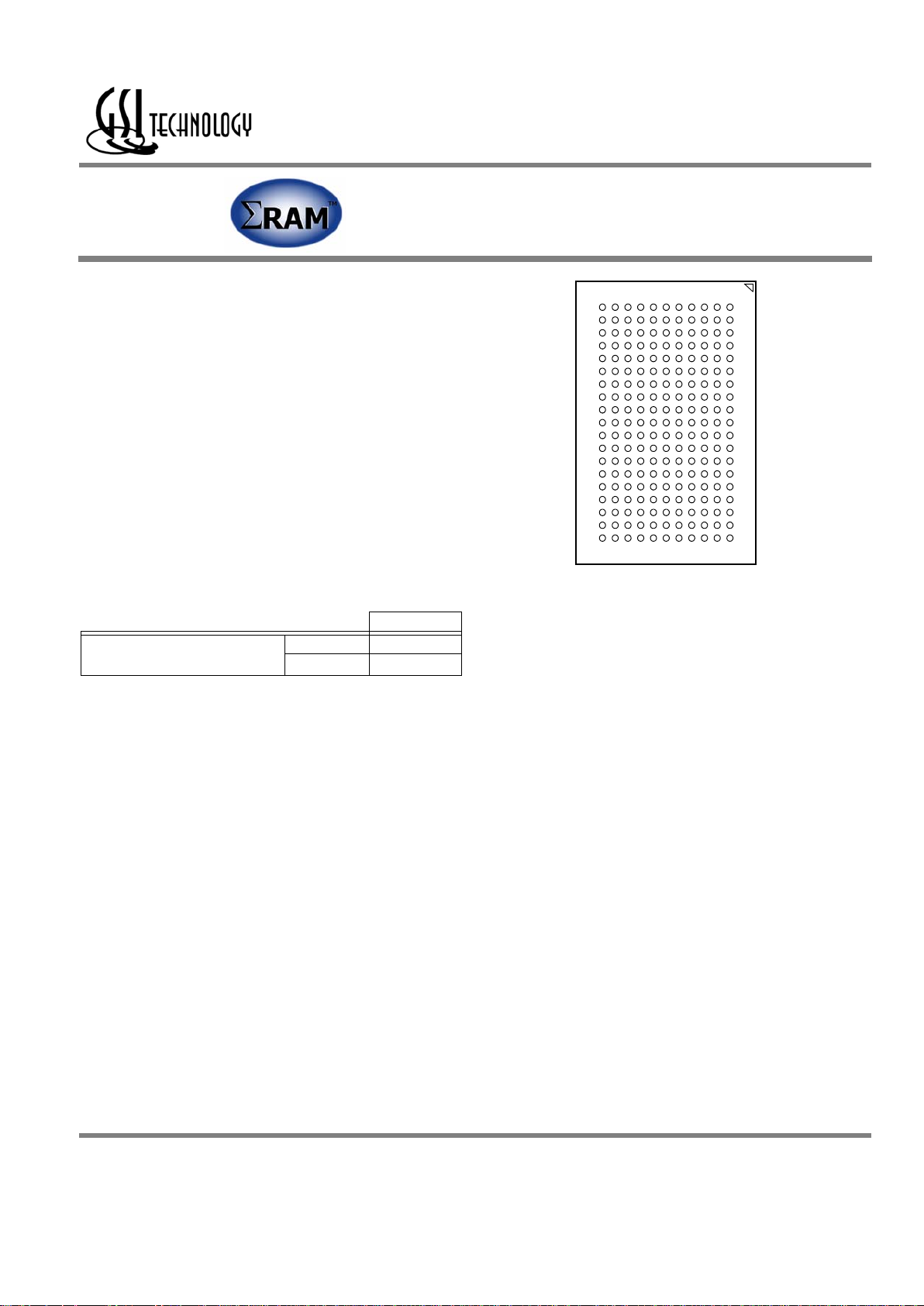
GS8170LW18/36/72C ΣRAMs are implemented with GSI's
high performance CMOS technology and are packaged in a
209-bump BGA.
- 333
Pipeline mode
tKHKH 3.0 ns
tKHQV 1.6 ns
209-Bump, 14 mm x 22 mm BGA
1 mm Bump Pitch, 11 x 19 Bump Array
Bottom View
Rev: 1.01 7/2002 2/33 © 2002, Giga Semiconductor, Inc.
Specifications cited are design targets and are subject to change without notice. For latest documentation contact your GSI representative.
Preliminary
GS8170LW18/36/72C-333/300/250
8170LW72C 256K x 72 Pinout
256K x 72 Common I/O—Top View
1234567891011
A DQg DQg A E2 A
ADV A
E3 A DQb DQb
B DQg DQg Bc
Bg NC W A Bb Bf DQb DQb
C DQg DQg Bh
Bd NC
(144M)
E1 NC Be Ba DQb DQb
D DQg DQg V
SS
NC NC MCL NC NC V
SS
DQb DQb
E DQg DQc V
DDQ
V
DDI
V
DD
V
DD
V
DD
V
DDI
V
DDQ
DQf DQb
FDQcDQcV
SS
V
SS
V
SS
ZQ V
SS
V
SS
V
SS
DQf DQf
G DQc DQc V
DDQ
V
DDQ
V
DD
EP2 V
DD
V
DDQ
V
DDQ
DQf DQf
H DQc DQc V
SS
V
SS
V
SS
EP3 V
SS
V
SS
V
SS
DQf DQf
J DQc DQc V
DDQ
V
DDQ
V
DD
MCH V
DD
V
DDQ
V
DDQ
DQf DQf
K CQ2 CQ2
CK NC V
SS
MCL V
SS
NC NC CQ1 CQ1
L DQh DQh V
DDQ
V
DDQ
V
DD
MCL V
DD
V
DDQ
V
DDQ
DQa DQa
M DQh DQh V
SS
V
SS
V
SS
MCL V
SS
V
SS
V
SS
DQa DQa
N DQh DQh V
DDQ
V
DDQ
V
DD
MCH V
DD
V
DDQ
V
DDQ
DQa DQa
P DQh DQh V
SS
V
SS
V
SS
MCL V
SS
V
SS
V
SS
DQa DQa
R DQd DQh V
DDQ
V
DDI
V
DD
V
DD
V
DD
V
DDI
V
DDQ
DQa DQe
T DQd DQd V
SS
NC NC MCL NC NC V
SS
DQe DQe
U DQd DQd NC A NC
(72M)
A NC
(36M)
A NC DQe DQe
VDQdDQdAAAA1AAADQe DQe
WDQdDQdTMS TDI AA0ATDO TCK DQe DQe
• 2001.03
11 x 19 Bump BGA—14 x 22 mm2 Body—1 mm Bump Pitch
Rev: 1.01 7/2002 3/33 © 2002, Giga Semiconductor, Inc.
Specifications cited are design targets and are subject to change without notice. For latest documentation contact your GSI representative.
Preliminary
GS8170LW18/36/72C-333/300/250
8170LW36C 512K x 36 Pinout
512K x 36 Common I/O—Top View
1234567891011
A NC NC A E2 A
ADV A E3 A DQb DQb
B NC NC Bc
NC A W A Bb NC DQb DQb
C NC NC NC Bd
NC
(144M)
E1 NC NC Ba DQb DQb
D NC NC V
SS
NC NC MCL NC NC V
SS
DQb DQb
E NC DQc V
DDQ
V
DDI
V
DD
V
DD
V
DD
V
DDI
V
DDQ
NC DQb
F DQc DQc V
SS
V
SS
V
SS
ZQ V
SS
V
SS
V
SS
NC NC
G DQc DQc V
DDQ
V
DDQ
V
DD
EP2 V
DD
V
DDQ
V
DDQ
NC NC
H DQc DQc V
SS
V
SS
V
SS
EP3 V
SS
V
SS
V
SS
NC NC
J DQc DQc V
DDQ
V
DDQ
V
DD
MCH V
DD
V
DDQ
V
DDQ
NC NC
K CQ2 CQ2
CK NC V
SS
MCL V
SS
NC NC CQ1 CQ1
L NC NC V
DDQ
V
DDQ
V
DD
MCL V
DD
V
DDQ
V
DDQ
DQa DQa
M NC NC V
SS
V
SS
V
SS
MCL V
SS
V
SS
V
SS
DQa DQa
N NC NC V
DDQ
V
DDQ
V
DD
MCH V
DD
V
DDQ
V
DDQ
DQa DQa
P NC NC V
SS
V
SS
V
SS
MCL V
SS
V
SS
V
SS
DQa DQa
R DQd NC V
DDQ
V
DDI
V
DD
V
DD
V
DD
V
DDI
V
DDQ
DQa NC
T DQd DQd V
SS
NC NC MCL NC NC V
SS
NC NC
U DQd DQd NC A NC (72M) A NC (36M) A NC NC NC
VDQdDQdAAAA1AAANC NC
WDQdDQdTMSTDI AA0ATDO TCK NC NC
• 2001.03
11 x 19 Bump BGA—14 x 22 mm2 Body—1 mm Bump Pitch
Rev: 1.01 7/2002 4/33 © 2002, Giga Semiconductor, Inc.
Specifications cited are design targets and are subject to change without notice. For latest documentation contact your GSI representative.
Preliminary
GS8170LW18/36/72C-333/300/250
8170LW18 1M x 18 Pinout
1M x 18 Common I/O—Top View
1234567891011
A NC NC A E2 A ADV A E3 A NC NC
B NC NC Bb
NC A W A NC NC NC NC
C NC NC NC NC NC
(144M)
E1
A NC Ba NC NC
D NC NC V
SS
NC NC MCL NC NC V
SS
NC NC
E NC DQb V
DDQ
V
DDI
V
DD
V
DD
V
DD
V
DDI
V
DDQ
NC NC
F DQb DQb V
SS
V
SS
V
SS
ZQ V
SS
V
SS
V
SS
NC NC
G DQb DQb V
DDQ
V
DDQ
V
DD
EP2 V
DD
V
DDQ
V
DDQ
NC NC
H DQb DQb V
SS
V
SS
V
SS
EP3 V
SS
V
SS
V
SS
NC NC
J DQb DQb V
DDQ
V
DDQ
V
DD
MCH V
DD
V
DDQ
V
DDQ
NC NC
K CQ2 CQ2
CK NC V
SS
MCL V
SS
NC NC CQ1 CQ1
L NC NC V
DDQ
V
DDQ
V
DD
MCL V
DD
V
DDQ
V
DDQ
DQa DQa
M NC NC V
SS
V
SS
V
SS
MCL V
SS
V
SS
V
SS
DQa DQa
N NC NC V
DDQ
V
DDQ
V
DD
MCH V
DD
V
DDQ
V
DDQ
DQa DQa
P NC NC V
SS
V
SS
V
SS
MCL V
SS
V
SS
V
SS
DQa DQa
R NC NC V
DDQ
V
DDI
V
DD
V
DD
V
DD
V
DDI
V
DDQ
DQa NC
T NC NC V
SS
NC NC MCL NC NC V
SS
NC NC
U NC NC NC A NC
(72M)
A NC
(36M)
A NC NC NC
VNCNCAAAA1AAANC NC
WNCNCTMSTDIAA0ATDO TCK NC NC
• 2001.03
11 x 19 Bump BGA—14 x 22 mm2 Body—1 mm Bump Pitch
Rev: 1.01 7/2002 5/33 © 2002, Giga Semiconductor, Inc.
Specifications cited are design targets and are subject to change without notice. For latest documentation contact your GSI representative.
Preliminary
GS8170LW18/36/72C-333/300/250
Pin Description Table
Symbol Description Type Comments
A Address Input —
ADV Advance Input Active High
Bx
Byte Write Enable Input Active Low
CK Clock Input Active High
CQ Echo Clock Output Active High
CQ
Echo Clock Output Active Low
DQ Data I/O Input/Output —
E1
Chip Enable Input Active Low
E2 & E3 Chip Enable Input Programmable Active High or Low
EP2 & EP3 Chip Enable Program Pin Input —
TCK Test Clock Input Active High
TDI Test Data In Input —
TDO Test Data Out Output —
TMS Test Mode Select Input —
MCH Must Connect High Input Active High
MCL Must Connect Low Input Active Low
NC No Connect — Not connected to die
W
Write Input Active Low
V
DD
Core Power Supply Input 1.8 V Nominal
V
DDQ
Output Driver Power Supply Input 1.8 V or 1.5 V Nominal
V
DDI
Input Buffer Power Supply Input 1.8 V or 1.5 V Nominal
V
SS
Ground Input —
ZQ Output Impedance Control Input
Low = Low Impedance [High Drive]
High = High Impedance [Low Drive]
Rev: 1.01 7/2002 6/33 © 2002, Giga Semiconductor, Inc.
Specifications cited are design targets and are subject to change without notice. For latest documentation contact your GSI representative.
Preliminary
GS8170LW18/36/72C-333/300/250
Background
The central characteristics of ΣRAMs are that they are extremely fast and consume very little power. Because both operating and
interface power is low, ΣRAMs can be implemented in a wide (x72) configuration, providing very high single package bandwidth
(in excess of 20Gb/s in ordinary pipelined configuration) and very low random access latency (5 ns). The use of very low voltage
circuits in the core and 1.8 V or 1.5 V interface voltages allow the speed, power and density performance of ΣRAMs.
The ΣRAM family of pinouts has been designed to support a number of different common read and write protocols. The following
timing diagrams provide a quick comparison between single data rate read and write protocols options available in the context of
the ΣRAM standard. This particular datasheet covers the single data rate (non-DDR), Late Write (LW) ΣRAM.
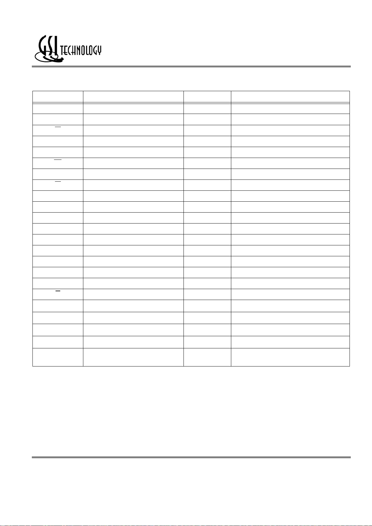
Common I/O SigmaRAM Family Mode Comparison—EW vs. LW vs. DLW
Note: R = Read, W = Write, Z = Deselect
The character of the applications for fast synchronous SRAMs in networking systems are extremely diverse. ΣRAMs have been
developed to address the broad variety of applications in the networking market in a manner that can be supported with a unified
development and manufacturing infrastructure. ΣRAMs address each of the bus protocol options commonly found in networking
systems. This allows the ΣRAM to find application in radical shrinks and speed-ups of existing networking chip sets that were
designed for use with older SRAMs, like the NBT, Late Write, or Double Data Rate SRAMs, as well as with new chip sets and
ASICs that employ the Echo Clocks and realize the full potential of the ΣRAMs.
Σ
1x1Ep (Early Write - Pipelined Read)
Σ
1x1Lp (Late Write - Pipelined Read)
Σ
1x1Dp (Double Late Write - Pipelined Read)
QE
DQ
QE
ABCDE F
F
Control
RXXWRR
BC E
CK
Address
CQ
D
DD
R
CK
QD
Address
A
QA DC
QA
R
DF
CK
CQ
W
Control
XZW
Address
ABC
Control
RWR
QC DD
DEF
WRW
CQ
QA DB
Rev: 1.01 7/2002 7/33 © 2002, Giga Semiconductor, Inc.
Specifications cited are design targets and are subject to change without notice. For latest documentation contact your GSI representative.
Preliminary
GS8170LW18/36/72C-333/300/250
All address, data and control inputs (with the exception of PE2, PE3, ZQ, and the mode pins, L6, M6, J6) are synchronized to
rising clock edges. Read and write operations must be initiated with the Advance/Load
pin (ADV) held low, in order to load the
new address. Device activation is accomplished by asserting all three of the Chip Enable inputs (E1
, E2, and E3). Deassertion of
any one of the Enable inputs will deactivate the device. It should be noted that ONLY deactivation of the RAM via E2 and/or
E3 deactivates the Echo Clocks, CQ1–CQ2.
Mode Selection Truth Table Standard
L6 M6 J6 Name Function Analogous to... In This Data Sheet?
000
Σ
1x1Ef
Early Write, Flow through Read Flow through Burst RAM No
001
Σ
1x1Lf
Late Write, Flow through Read Flow through NBT SRAM No
010 RFU n/a
011
Σ
1x2Lp
DDR Double Data Rate SRAM No
100
Σ
1x1Ep
Early Write, Pipeline Read Pipelined Burst RAM No
101
Σ
1x1Dp
Double Late Write, Pipeline Read Pipelined NBT SRAM No
110
Σ
1x1Lp
Late Write, Pipeline Read Pipelined Late Write SRAM Yes
111 RFU — n/a
Rev: 1.01 7/2002 8/33 © 2002, Giga Semiconductor, Inc.
Specifications cited are design targets and are subject to change without notice. For latest documentation contact your GSI representative.
Preliminary
GS8170LW18/36/72C-333/300/250
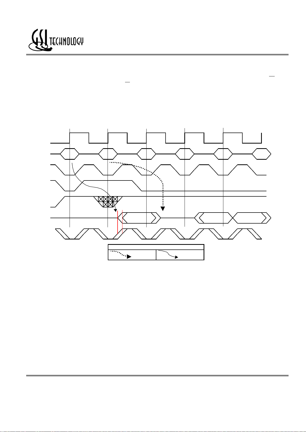
Read Operations
Pipelined Read
Read operation is initiated when the following conditions are satisfied at the rising edge of clock: All three chip enables (E1, E2,
and E3) are active, the write enable input signal (W
) is deasserted high, and ADV is asserted low. The address presented to the
address inputs is latched into the address register and presented to the memory core and control logic. The control logic determines
that a read access is in progress and allows the requested data to propagate to the input of the output register. At the next rising edge
of clock the read data is allowed to propagate through the output register and onto the output pins.
Single Data Rate Pipelined Read
FDAddress
Read
CK
E
QC QD
CQ
Read Deselect Read Read
AXXC
Key
Hi-Z Access
ADV
QA
/E
1
/W
DQ
Rev: 1.01 7/2002 9/33 © 2002, Giga Semiconductor, Inc.
Specifications cited are design targets and are subject to change without notice. For latest documentation contact your GSI representative.
Preliminary
GS8170LW18/36/72C-333/300/250
Write Operations
Write operation occurs when the following conditions are satisfied at the rising edge of clock: All three chip enables (E1, E2, and
E3) are active, the write enable input signal (W
) is asserted low, and ADV is asserted low.
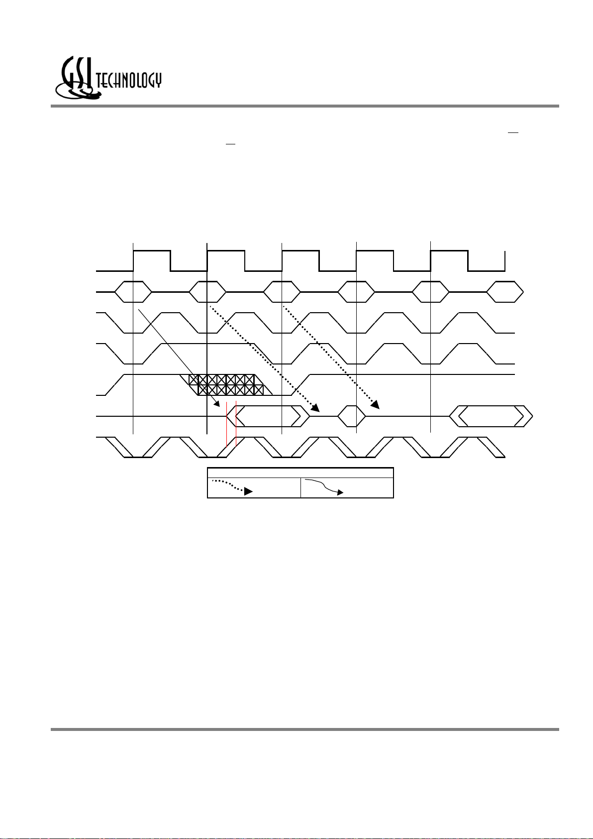
Late Write
In Late Write mode the RAM requires Data In one rising clock edge later than the edge used to load Address and Control. Late
Write protocol has been employed on SRAMs designed for RISC processor L2 cache applications.
SigmaRAM Late Write with Pipelined Read
Key
QDQA D
C
CQ
Read Read
CDE
ADV
Read Deselect Write
Hi-Z
F
Access
CK
Address A XX
/E
1
/W
DQ
Rev: 1.01 7/2002 10/33 © 2002, Giga Semiconductor, Inc.
Specifications cited are design targets and are subject to change without notice. For latest documentation contact your GSI representative.
Preliminary
GS8170LW18/36/72C-333/300/250
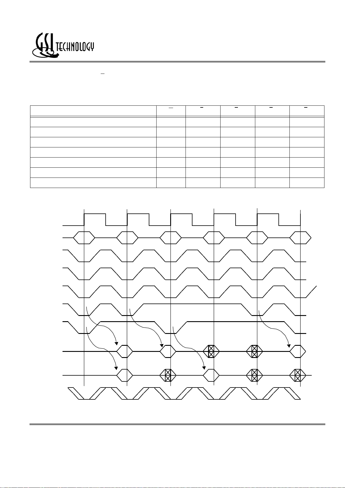
Byte Write Control
The Byte Write Enable inputs (BX) determine which bytes will be written. All or none may be activated. A Write Cycle with no
Byte Write inputs active is a write abort cycle.
Byte Write Control Example with x18 SigmaRAM Late Write RAM
Example of x36 Byte Write Truth Table
Function W
B
A
B
B
B
C
B
D
Read HXXXX
Write Byte A L L H H H
Write Byte B L H L H H
Write Byte C L H H L H
Write Byte D L H H H L
Write all Bytes L L L L L
Write Abort L H H H H
DA DB DE
DA DC
F
/E
1
Write
BCD
ADV
ADV
Non-WriteWrite Write
CK
Address A E
Write
CQ
/BA
/BB
DQA0-DQA8
DQB0-DQB8
 Loading...