

GSI GS8170DD18C-300I, GS8170DD18C-300, GS8170DD18C-250I, GS8170DD18C-250, GS8170DD36C-333I Datasheet
...
Rev: 1.00e 6/2002 1/31 © 2002, GSI Technology, Inc.
Specifications cited are design targets and are subject to change without notice. For latest documentation contact your GSI representative.
Preliminary
GS8170DD18/36C-333/300/250
18Mb Σ1x2Lp Double Data Rate
SigmaRAM™ SRAM
250 MHz–333 MHz
1.8 V V
DD
1.8 V and 1.5 V I/O
209-Bump BGA
Commercial Temp
Industrial Temp
Features
• Double Data Rate Read and Write mode
• JEDEC-standard SigmaRAM
™
pinout and package
• 1.8 V +150/–100 mV core power supply
• 1.5 V or 1.8 V I/O supply
• Pipelined read operation
• Fully coherent read and write pipelines
• Echo Clock outputs track data output drivers
• ZQ mode pin for user-selectable output drive strength
• 2 user-programmable chip enable inputs for easy depth
expansion
• IEEE 1149.1 JTAG-compatible Boundary Scan
• 209-bump, 14 mm x 22 mm, 1 mm bump pitch BGA package
• Pin-compatible with future 36Mb, 72Mb, and 144Mb devices
SigmaRAM Family Overview
GS8170DD18/36 SigmaRAMs are built in compliance with
the SigmaRAM pinout standard for synchronous SRAMs.
They are 18,874,368-bit (18Mb) SRAMs. These are the first in
a family of wide, very low voltage CMOS I/O SRAMs
designed to operate at the speeds needed to implement
economical high performance networking systems.
GSI's ΣRAMs are offered in a number of configurations that
emulate other synchronous SRAMs, such as Burst RAMs,
NBT, Late Write, or Double Data Rate (DDR) SRAMs. The
logical differences between the protocols employed by these
RAMs hinge mainly on various combinations of address
bursting, output data registering and write cueing. The
ΣRAM
™
family standard allows a user to implement the
interface protocol best suited to the task at hand.
Functional Description
Because SigmaRAMs are synchronous devices, address and
read/write control inputs are captured on the rising edge of the
input clock. Write cycles are internally self-timed and initiated
by the rising edge of the clock input. This feature eliminates
complex off-chip write pulse generation required by
asynchronous SRAMs and simplifies input signal timing. In
DDR mode the device captures Data In on both rising and
falling edges of clock and drives data on both clock edges as
well.
Because the DDR ΣRAM always transfers data in two halves,
A0 is internally set to 0 for the first half of each read or write
transfer, and automatically incremented to 1 for the falling
edge transfer. The address field of a DDR ΣRAM is always one
address pin less than the advertised index depth (e.g., the 1M x
18 has a 512k addressable index).
In Pipeline mode, Single Data Rate (SDR) ΣRAMs incorporate
a rising-edge-triggered output register. In DDR mode, risingand falling-edge-triggered output registers are employed. For
read cycles, a DDR SRAM’s output data is staged at the input
of an edge-triggered output register during the access cycle and
then released to the output drivers at the next rising and
subsequent falling edge of clock.
GS817x18/36/72B ΣRAMs are implemented with GSI's high
performance CMOS technology and are packaged in a 209bump BGA.
- 333
Pipeline mode
tKHKH 3.0 ns
tKHQV 1.6 ns
209-Bump, 14 mm x 22 mm BGA
1 mm Bump Pitch, 11 x 19 Bump Array
Bottom View
Rev: 1.00e 6/2002 2/31 © 2002, GSI Technology, Inc.
Specifications cited are design targets and are subject to change without notice. For latest documentation contact your GSI representative.
Preliminary
GS8170DD18/36C-333/300/250
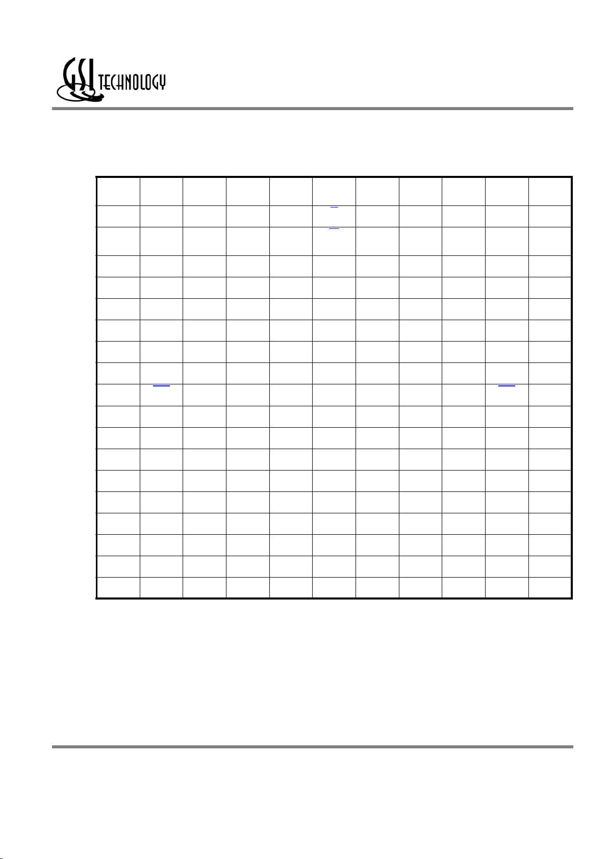
8170DD36 512K x 36 Pinout
512K x 36 Common I/O—Top View
1234567891011
A NC NC A E2 A
ADV A E3 A DQb DQb
B NC NC
MCL
NC A W
A
MCL
NC DQb DQb
C NC NC NC MCL NC
(144M)
E1
NC NC MCL DQb DQb
D NC NC V
SS
NC NC MCL NC NC V
SS
DQb DQb
E NC DQc V
DDQ
V
DDI
V
DD
V
DD
V
DD
V
DDI
V
DDQ
NC DQb
F DQc DQc V
SS
V
SS
V
SS
ZQ V
SS
V
SS
V
SS
NC NC
G DQc DQc V
DDQ
V
DDQ
V
DD
EP2 V
DD
V
DDQ
V
DDQ
NC NC
H DQc DQc V
SS
V
SS
V
SS
EP3 V
SS
V
SS
V
SS
NC NC
J DQc DQc V
DDQ
V
DDQ
V
DD
MCH V
DD
V
DDQ
V
DDQ
NC NC
K CQ2 CQ2
CK NC V
SS
MCL V
SS
NC NC CQ1 CQ1
L NC NC V
DDQ
V
DDQ
V
DD
MCL V
DD
V
DDQ
V
DDQ
DQa DQa
M NC NC V
SS
V
SS
V
SS
MCH V
SS
V
SS
V
SS
DQa DQa
N NC NC V
DDQ
V
DDQ
V
DD
MCH V
DD
V
DDQ
V
DDQ
DQa DQa
P NC NC V
SS
V
SS
V
SS
MCL V
SS
V
SS
V
SS
DQa DQa
R DQd NC V
DDQ
V
DDI
V
DD
V
DD
V
DD
V
DDI
V
DDQ
DQa NC
T DQd DQd V
SS
NC NC MCL NC NC V
SS
NC NC
U DQd DQd NC A NC (72M) A NC (36M) A NC NC NC
VDQdDQdAAAA1AAANC NC
WDQdDQdTMSTDI A MCL A TDO TCK NC NC
• 2001.03
11 x 19 Bump BGA—14 x 22 mm2 Body—1 mm Bump Pitch
Rev: 1.00e 6/2002 3/31 © 2002, GSI Technology, Inc.
Specifications cited are design targets and are subject to change without notice. For latest documentation contact your GSI representative.
Preliminary
GS8170DD18/36C-333/300/250
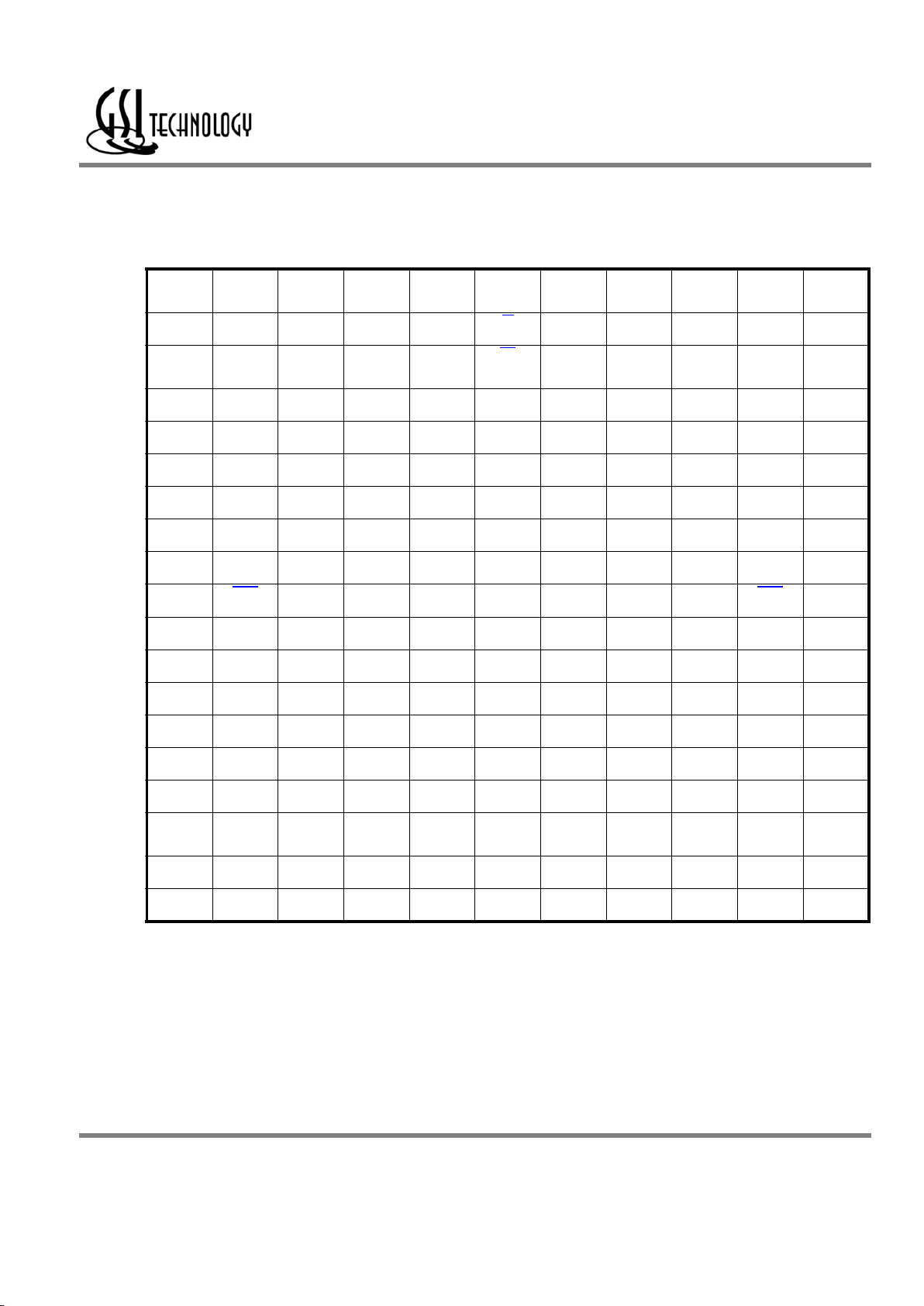
8170DD18 1M x 18 Pinout
1M x 18 Common I/O—Top View
1234567891011
A NC NC A E2 A ADV A E3 A NC NC
B NC NC
MCL
NC A W
A NC NC NC NC
C NC NC NC NC NC
(144M)
E1
A NC MCL NC NC
D NC NC V
SS
NC NC MCL NC NC V
SS
NC NC
E NC DQb V
DDQ
V
DDI
V
DD
V
DD
V
DD
V
DDI
V
DDQ
NC NC
F DQb DQb V
SS
V
SS
V
SS
ZQ V
SS
V
SS
V
SS
NC NC
G DQb DQb V
DDQ
V
DDQ
V
DD
EP2 V
DD
V
DDQ
V
DDQ
NC NC
H DQb DQb V
SS
V
SS
V
SS
EP3 V
SS
V
SS
V
SS
NC NC
J DQb DQb V
DDQ
V
DDQ
V
DD
MCH V
DD
V
DDQ
V
DDQ
NC NC
K CQ2 CQ2
CK NC V
SS
MCL V
SS
NC NC CQ1 CQ1
L NC NC V
DDQ
V
DDQ
V
DD
MCL V
DD
V
DDQ
V
DDQ
DQa DQa
M NC NC V
SS
V
SS
V
SS
MCH V
SS
V
SS
V
SS
DQa DQa
N NC NC V
DDQ
V
DDQ
V
DD
MCH V
DD
V
DDQ
V
DDQ
DQa DQa
P NC NC V
SS
V
SS
V
SS
MCL V
SS
V
SS
V
SS
DQa DQa
R NC NC V
DDQ
V
DDI
V
DD
V
DD
V
DD
V
DDI
V
DDQ
DQa NC
T NC NC V
SS
NC NC MCL NC NC V
SS
NC NC
U NC NC NC A NC
(72M)
A NC
(36M)
A NC NC NC
VNCNCAAAA1AAANC NC
WNCNCTMSTDIA MCL A TDO TCK NC NC
• 2001.03
11 x 19 Bump BGA—14 x 22 mm2 Body—1 mm Bump Pitch
Rev: 1.00e 6/2002 4/31 © 2002, GSI Technology, Inc.
Specifications cited are design targets and are subject to change without notice. For latest documentation contact your GSI representative.
Preliminary
GS8170DD18/36C-333/300/250
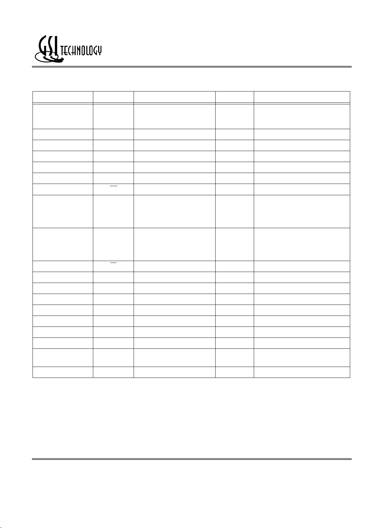
Pin Description Table
Pin Location Symbol Description Type Comments
A3, A5, A7, A9, B7, U4,
U6, U8, V3, V4, V5, V6,
V7, V8, V9, W5, W7
A Address Input —
C7 A Address Input x18 version only
B5 A Address Input x18 and x36 versions
A6 ADV Advance Input Active High
K3 CK Clock Input Active High
K1, K11 CQ Echo Clock Output Active High
K2, K10 CQ
Echo Clock Output Active Low
E2, F1, F2, G1, G2, H1,
H2, J1, J2, L10, L11,
M10, M11, N10, N11,
P10, P11, R10
DQ Data I/O Input/Output x18 and x36 versions
A10, A11, B10, B11,
C10, C11, D10, D11,
E11, R1, T1, T2, U1, U2,
V1, V2, W1, W2
DQ Data I/O Input/Output x36 version
C6 E1
Chip Enable Input Active Low
A4, A8 E2 & E3 Chip Enable Input Programmable Active High or Low
G6, H6 EP2 & EP3 Chip Enable Program Pin Input —
W9 TCK Test Clock Input Active High
W4 TDI Test Data In Input —
W8 TDO Test Data Out Output —
W3 TMS Test Mode Select Input —
J6, M6, N6 MCH Must Connect High Input Active High (all versions)
B3, C9, D6, K6, L6, P6,
T6, W6
MCL Must Connect Low Input Active Low (all versions)
B8, C4 MCL Must Connect Low Input Active Low (x36 version)
Rev: 1.00e 6/2002 5/31 © 2002, GSI Technology, Inc.
Specifications cited are design targets and are subject to change without notice. For latest documentation contact your GSI representative.
Preliminary
GS8170DD18/36C-333/300/250
A1, A2, B1, B2, B4, B9,
C1, C2, C3, C5, C8, D1,
D2, D4, D5, D7, D8,E1,
E10, F10, F11, G10,
G11, H10, H11, J10, J11,
K4, K8, K9, L1, L2, M1,
M2, N1, N2, P1, P2, R2,
R11, T4, T5, T7, T8, T10,
T11, U3, U5, U7, U9,
U10, U11, V10, V11,
W10, W11
NC No Connect — Not connected to die (all versions)
C7 NC No Connect — Not connected to die (x36 version)
A1, A2, B1, B2, B4, B9,
C1, C2, C3, C8, D1, D2,
E1, E10, F10, F11, G10,
G11, H10, H11, J10, J11,
L1, L2, M1, M2, N1, N2,
P1, P2, R2, R11, T10,
T11, U10, U11, V10,
V11, W10, W11
NC No Connect — Not connected to die (x36/x18 versions)
A10, A11, B8, B10, B11,
C4, C10, C11, D10, D11,
E11, R1, T1, T2, U1, U2,
V1, V2, W1, W2
NC No Connect — Not connected to die (x18 version)
B6 W
Write Input Active Low
E5, E6, E7, G5, G7, J5,
J7, L5, L7, N5, N7, R5,
R6, R7
V
DD
Core Power Supply Input 1.8 V Nominal
E3, E4, E8, E9, J3, J4,
J8, J9, L3, L4, L8, L9,
N3, N4, N8, N9, R3, R4,
R8, R9
V
DDQ
Output Driver Power Supply Input 1.8 V or 1.5 V Nominal
E4, E8, R4, R8
V
DDI
Input Buffer Power Supply Input 1.8 V or 1.5 V Nominal
D3, D9, F3, F4, F5, F7,
F8, F9, H3, H4, H5, H7,
H8, H9, K5, K7, M3, M4,
M5, M7, M8, M9, P3, P4,
P5, P7, P8, P9, T3, T9
V
SS
Ground Input —
F6 ZQ Output Impedance Control Input
Low = Low Impedance [High Drive]
High = High Impedance [Low Drive]
Pin Description Table
Pin Location Symbol Description Type Comments
Rev: 1.00e 6/2002 6/31 © 2002, GSI Technology, Inc.
Specifications cited are design targets and are subject to change without notice. For latest documentation contact your GSI representative.
Preliminary
GS8170DD18/36C-333/300/250
Background
The central characteristics of ΣRAMs are that they are extremely fast and consume very little power. Because both operating and
interface power is low, ΣRAMs can be implemented in a wide (x36) configuration, providing very high single package bandwidth
(in excess of 20 Gb/s in ordinary pipelined configuration) and very low random access latency (5 ns). The use of very low voltage
circuits in the core and 1.8 V or 1.5 V interface voltages allow the speed, power and density performance of ΣRAMs.
The ΣRAM family of pinouts has been designed to support a number of different common read and write protocols. The following
timing diagrams provide a quick comparison between the late write read and write protocol and the DDR protocol options available
in the context of the ΣRAM standard. This particular datasheet covers the Double Data Rate (DDR) ΣRAM.
The character of the applications for fast synchronous SRAMs in networking systems are extremely diverse. ΣRAMs have been
developed to address the broad variety of applications in the networking market in a manner that can be supported with a unified
development and manufacturing infrastructure. ΣRAMs address each of the bus protocol options commonly found in networking
systems. This allows the ΣRAM to find application in radical shrinks and speed-ups of existing networking chip sets that were
designed for use with older SRAMs, like the NBT, Late Write, or Double Data Rate SRAMs, as well as with new chip sets and
ASIC’s that employ the Echo Clocks and realize the full potential of the ΣRAMs.
All address and control inputs (with the exception of PE2, PE3, ZQ, and the mode pins, L6, M6, and J6) are synchronized to rising
clock edges. Data in is captured on both rising and falling edges of CK. Read and write operations must be initiated with the
Advance/Load
pin (ADV) held low, in order to load the new address. Device activation is accomplished by asserting all three of the
Chip Enable inputs (E1
, E2, and E3). Deassertion of any one of the Enable inputs will deactivate the device. It should be noted
that ONLY deactivation of the RAM via E2 and/or E3 deactivates the Echo Clocks, CQ1–CQ2.
Mode Selection Truth Table Standard
L6 M6 J6 Name Function Analogous to... In This Data Sheet?
000
Σ
1x1Ef
Early Write, Flow through Read Flow through Burst RAM No
001
Σ
1x1Lf
Late Write, Flow through Read Flow through NBT SRAM No
010 RFU n/a
011
Σ
1x2Lp
DDR Double Data Rate SRAM Yes
100
Σ
1x1Ep
Early Write, Pipelined Read Pipelined Burst RAM No
101
Σ
1x1Dp
Double Late Write, Pipelined Read Pipelined NBT SRAM No
110
Σ
1x1Lp
Late Write, Pipelined Read Pipelined Late Write SRAM No
Rev: 1.00e 6/2002 7/31 © 2002, GSI Technology, Inc.
Specifications cited are design targets and are subject to change without notice. For latest documentation contact your GSI representative.
Preliminary
GS8170DD18/36C-333/300/250
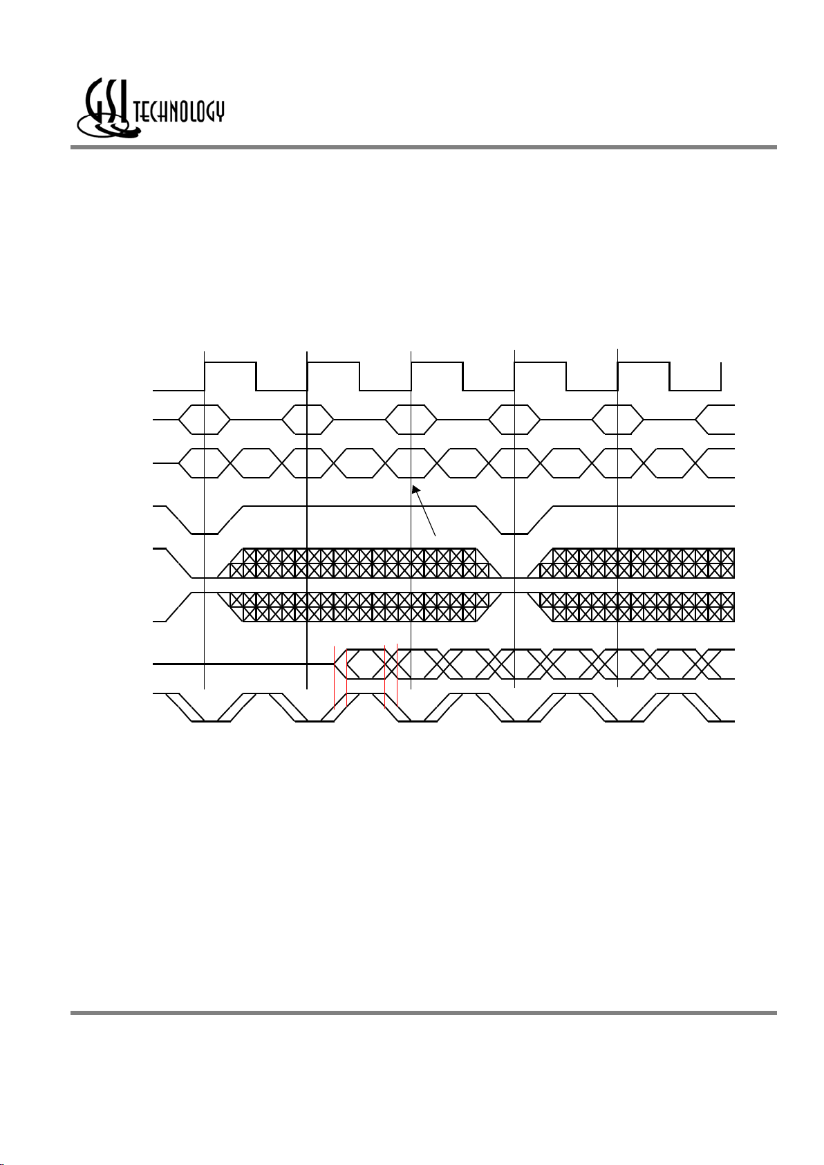
Read Operations
Double Data Rate Read
In applications where a data rate markedly faster than the RAM’s latency is desired, Double Data Rate reads double the data
transfer rate (read or write bandwidth) achieved in Pipeline mode while keeping the RAM’s clock frequency constant. In Double
Data Rate mode, the RAM multiplexes the results of a read out of the RAM on half the usual number of data pins. The output
register/mux behaves just as if it were in Pipeline mode for the first transfer, but then makes a second transfer in response to the
next falling edge of clock as well. SigmaRAM DDR RAMs burst in linear order only.
Double Data Rate Pipelined Read
QA0 QA1 QC0 QC1 QD0 QD1
CK
Read Deselect
AXX F
Read Read Read
ADV
DEC
/E
1
/W
DQ
Address
CQ
Key
Hi-Z Access
Rev: 1.00e 6/2002 8/31 © 2002, GSI Technology, Inc.
Specifications cited are design targets and are subject to change without notice. For latest documentation contact your GSI representative.
Preliminary
GS8170DD18/36C-333/300/250
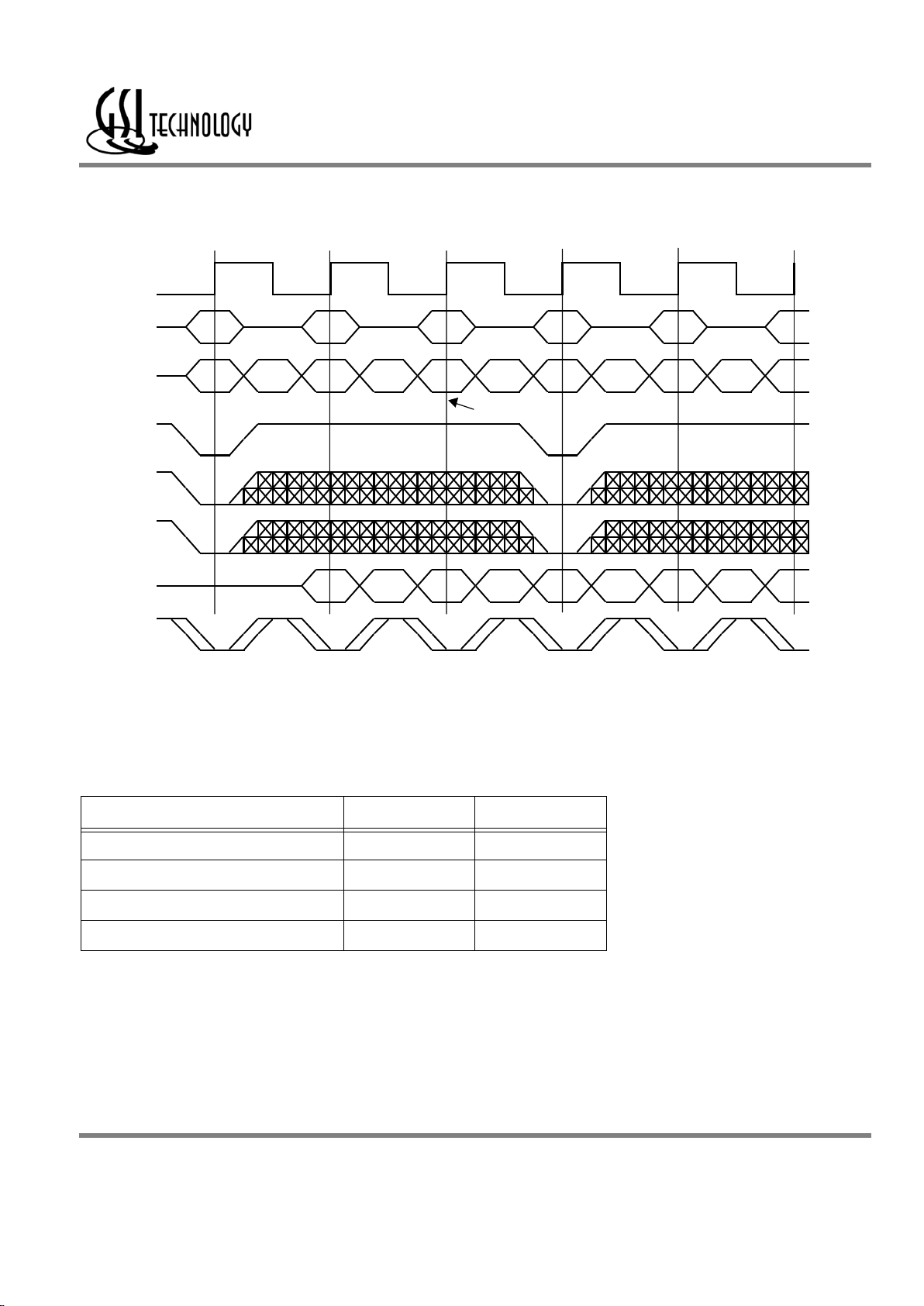
Write Operations
Write operation occurs when the following conditions are satisfied at the rising edge of clock: All three chip enables (E1, E2, and
E3) are active, the write enable input signal (W
) is asserted low, and ADV is asserted low.
Double Data Rate Write
A Double Data Rate Write is a specialized form of Late Write. In Double Data Rate mode, the RAM will capture Data In on both
rising and falling edges of the RAM clock, CK, beginning with the rising edge of clock that follows the capture of the write address
and command.
SigmaRAM Double Data Rate Read and Write
QA0 QA1 DC0 DC1 QD0 QD1
ADV
Read
CQ
E
Deselect
CD
Write ReadRead
CK
Address A
Key
Hi-Z Access
/E
1
/W
DQ
FB
Rev: 1.00e 6/2002 9/31 © 2002, GSI Technology, Inc.
Specifications cited are design targets and are subject to change without notice. For latest documentation contact your GSI representative.
Preliminary
GS8170DD18/36C-333/300/250
Special Functions
Burst Cycles
ΣRAMs provide an on-chip burst address generator that can be utilized, if desired, to further simplify burst read or write
implementations. The ADV control pin, when driven high, commands the SRAM to advance the internal address counter and use
the counter generated address to read or write the SRAM. The starting address for the first cycle in a burst cycle series is loaded
into the SRAM by driving the ADV pin low, into Load mode.
SigmaRAM DDR Burst Read with Counter Wrap-around
Counter Wraps
QA2 QA3 QA0 QA1 QA2 QA3 QB0 QB1
ADV
B3A2 B0
CQ
DQ
/E
1
/W
XX
Internal
Address
A2 A0 B2 B1A3
Continue
A1 A3 B 1
B0
CK
XX
Read Continue
Extern al
Address
A2 XX XX
Continue Read
Rev: 1.00e 6/2002 10/31 © 2002, GSI Technology, Inc.
Specifications cited are design targets and are subject to change without notice. For latest documentation contact your GSI representative.
Preliminary
GS8170DD18/36C-333/300/250
Burst Order
The burst address counter wraps around to its initial state after four internal addresses (the loaded address and three more) have
been accessed. SigmaRAMs always count in linear burst order.
Linear Burst Order
Notes:
1. The burst counter wraps to initial state on the 3rd rising edge of clock.
2. The DDR SigmaRAM always begins an read or write at A0 = 0. A0 is internally set to 0 at the rising edge of clock and is not
available to the user.
A[1:0] A[1:0]
1st address (Rising Edge CK) 00 10
2nd address (Falling Edge CK) 01 11
3rd address (Rising Edge CK) 10 00
4th address (Falling Edge CK) 11 01
SigmaRAM DDR Burst Write with Counter Wrap-around
ADV
DB2
CQ
DA2 DA3 DA0 DA1 DA2 DA3 DB0 DB1
/E
1
/W
DQ
B2 B3 B1
Counter Wraps
XX
Internal
Address
A2 A3 A0 A1 A2 A3 B 0 B 1
XX B0 XX
Write Continue Continue Write Continue
CK
Extern al
Address
A2 XX
 Loading...