

GSI GS8162Z72C-133I, GS8162Z72C-133, GS8162Z36D-250I, GS8162Z36D-250, GS8162Z36D-225I Datasheet
...
GS8162Z18(B/D)/GS8162Z36(B/D)/GS8162Z72(C)
119, 165, & 209 BGA
18Mb Pipelined and Flow Through
Commercial Temp
Industrial Temp
Synchronous NBT SRAM
Features
• NBT (No Bus Turn Around) functionality allows zero wait
Read-Write-Read bus utilization; fully pin-compatible with
both pipelined and flow through NtRAM™, NoBL™ and
ZBT™ SRAMs
• 2.5 V or 3.3 V +10%/–10% core power supply
• 2.5 V or 3.3 V I/O supply
• User-configurable Pipeline and Flow Through mode
• ZQ mode pin for user-selectable high
• IEEE 1149.1 JTAG-compatible Boundary Scan
• On-chip write parity checking; even or odd selectable
• On-chip parity encoding and error detection
• LBO
pin for Linear or Interleave Burst mode
• Pin-compatible with 2M, 4M, and 8M devices
• Byte write operation (9-bit Bytes)
• 3 chip enable signals for easy depth expansion
• ZZ Pin for automatic power-down
• JEDEC-standard 119-, 165-, or 209-Bump BGA package
/low output drive
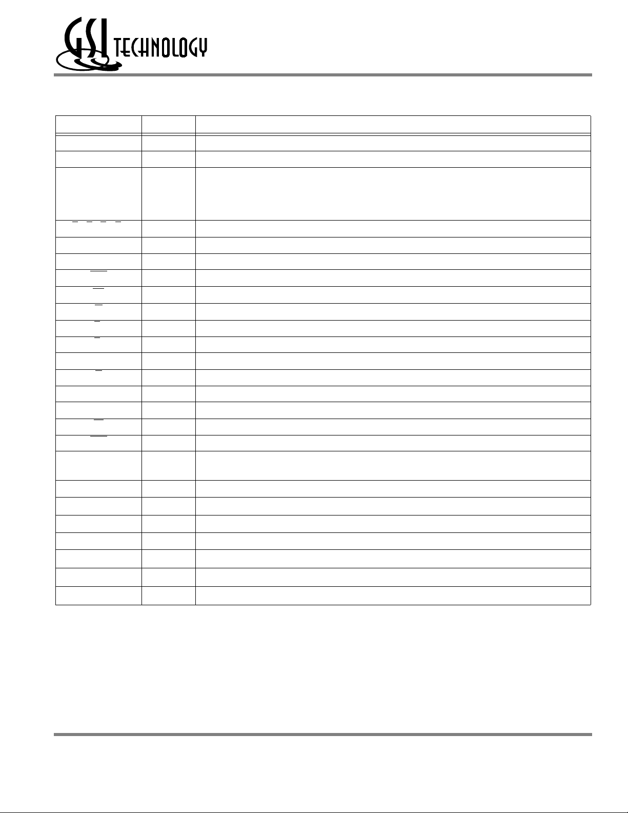
250 MHz–133 MHz
2.5 V or 3.3 V V
DD
2.5 V or 3.3 V I/O
read/write control inputs are captured on the rising edge of the
input clock. Burst order control (LBO
rail for proper operation. Asynchronous inputs include the
Sleep mode enable (ZZ) and Output Enable. Output Enable can
be used to override the synchronous control of the output
drivers and turn the RAM's output drivers off at any time.
Write cycles are internally self-timed and initiated by the rising
edge of the clock input. This feature eliminates complex offchip write pulse generation required by asynchronous SRAMs
and simplifies input signal timing.
The GS8162Z18(B/D)/36(B/D)/72(C) may be configured by
the user to operate in Pipeline or Flow Through mode.
Operating as a pipelined synchronous device, in addition to the
rising-edge-triggered registers that capture input signals, the
device incorporates a rising edge triggered output register. For
read cycles, pipelined SRAM output data is temporarily stored
by the edge-triggered output register during the access cycle
and then released to the output drivers at the next rising edge of
clock.
) must be tied to a power
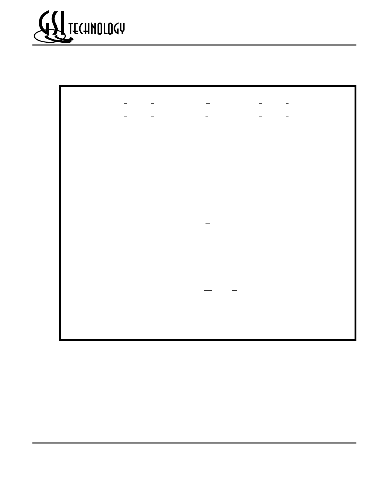
-250 -225 -200 -166 -150 -133 Unit
Pipeline
3-1-1-1
3.3 V
2.5 V
Flow
Through
2-1-1-1
3.3 V
2.5 V
t
KQ
tCycle
Curr (x18)
Curr (x36)
Curr (x72)
Curr (x18)
Curr (x36)
Curr (x72)
t
KQ
tCycle
Curr (x18)
Curr (x36)
Curr (x72)
Curr (x18)
Curr (x36)
Curr (x72)
2.5
4.0
280
330
n/a
275
320
n/a
5.5
5.5
175
200
n/a
175
200
n/a
2.7
4.4
255
300
n/a
250
295
n/a
6.0
6.0
165
190
n/a
165
190
n/a
3.0
5.0
230
270
350
230
265
335
6.5
6.5
160
180
225
160
180
225
3.4
6.0
200
230
300
195
225
290
7.0
7.0
150
170
115
150
170
115
3.8
6.7
185
215
270
180
210
260
7.5
7.5
145
165
210
145
165
210
4.0
7.5nsns
165
mA
190
mA
245
mA
165
mA
185
mA
235
mA
8.5
8.5nsns
135
mA
150
mA
185
mA
135
mA
150
mA
185
mA
Functional Description
The GS8162Z18(B/D)/36(B/D)/72(C) is an 18Mbit
Synchronous Static SRAM. GSI's NBT SRAMs, like ZBT,
NtRAM, NoBL or other pipelined read/double late write or
flow through read/single late write SRAMs, allow utilization
of all available bus bandwidth by eliminating the need to insert
deselect cycles when the device is switched from read to write
cycles.
The GS8162Z18(B/D)/36(B/D)/72(C) is implemented with
GSI's high performance CMOS technology and is available in
a JEDEC-standard 119-bump (x18 & x36), 165-bump (x18 &
x36), or 209-bump (x72) BGA package.
Because it is a synchronous device, address, data inputs, and
Rev: 2.18a 12/2002 1/38 © 1999, Giga Semiconductor, Inc.
Specifications cited are subject to change without notice. For latest documentation see http://www.gsitechnology.com.
NoBL is a trademark of Cypress Semiconductor Corp.. NtRAM is a trademark of Samsung Electronics Co.. ZBT is a trademark of Integrated Device Technology, Inc.
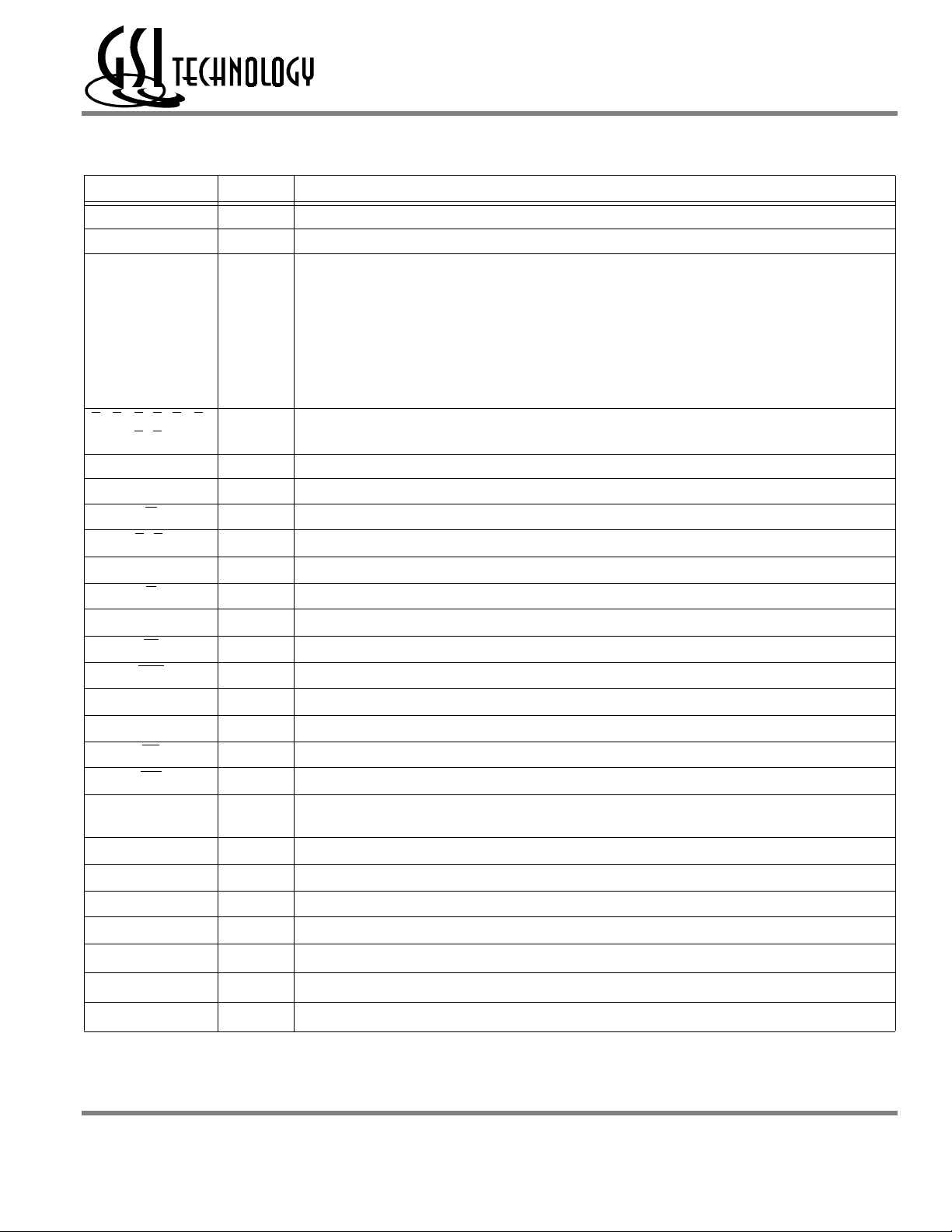
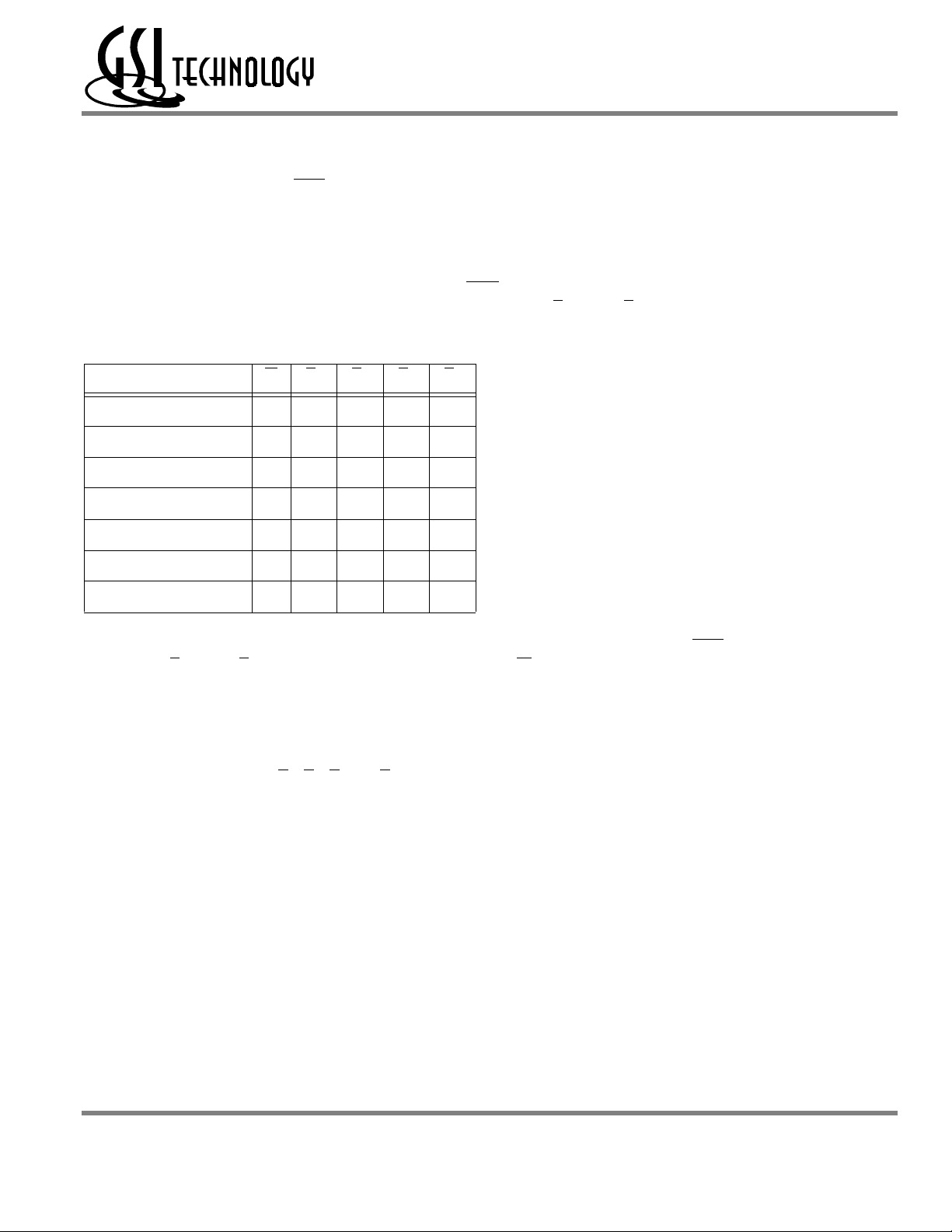
GS8162Z72 Pad Out
1234567891011
GS8162Z18(B/D)/GS8162Z36(B/D)/GS8162Z72(C)
209-Bump BGA—Top View (Package C)
A DQG5 DQG1 A13 E2 A14 ADV A15 E
B DQG6 DQG2 B
C DQG7 DQG3 B
D DQG8 DQG4 V
E DQG9 DQC9 V
F DQC4 DQC8 V
G DQC3 DQC7 V
H DQC2 DQC6 V
J DQC1 DQC5 V
K NC NC CK NC V
L DQH1 DQH5 V
M DQH2 DQH6 V
N DQH3 DQH7 V
P DQH4 DQH8 V
CBGNC WA16 BBBF DQB2 DQB6
HBDNCE1NCBEBA DQB3 DQB7
SS
DDQ
SS
DDQ
SS
DDQ
DDQ
SS
DDQ
SS
NC NC G NC NC V
V
DDQ
V
SS
V
DDQ
V
SS
V
DDQ
V
DDQ
V
SS
V
DDQ
V
SS
V
DD
V
SS
V
DD
V
SS
V
DD
SS
V
DD
V
SS
V
DD
V
SS
V
DD
ZQ V
MCH V
MCL V
MCH V
MCL V
FT V
MCL V
MCH V
ZZ V
V
DD
SS
DD
SS
DD
SS
DD
SS
DD
SS
V
V
V
V
V
3 A17 DQB1 DQB5
SS
DDQ
V
SS
DDQ
V
SS
DDQ
V
DDQ
V
SS
V
DDQ
V
SS
V
DDQ
DQB4 DQB8
DQF9 DQB9
DQF8 DQF4
DQF7 DQF3
DQF6 DQF2
DQF5 DQF1
NC NC NC NC
DDQ
V
SS
DDQ
V
SS
V
DDQ
V
SS
V
DDQ
V
SS
DQA5 DQA1
DQA6 DQA2
DQA7 DQA3
DQA8 DQA4
R DQD9 DQH9 V
T DQD8 DQD4 V
DDQ
SS
V
DDQ
NC NC LBO PE NC V
V
DD
V
DD
V
DD
V
DDQ
V
DDQ
SS
DQA9 DQE9
DQE4 DQE8
U DQD7 DQD3 NC A12 NC A11 NC A10 NC DQE3 DQE7
VDQD6DQD2A9A8A7A1A6A5A4DQE2DQE6
W DQD5 DQD1 TMS TDI A3 A0 A2 TDO TCK DQE1 DQE5
Rev 10
11 x 19 Bump BGA—14 x 22 mm
2
Body—1 mm Bump Pitch
Rev: 2.18a 12/2002 2/38 © 1999, Giga Semiconductor, Inc.
Specifications cited are subject to change without notice. For latest documentation see http://www.gsitechnology.com.
GS8162Z18(B/D)/GS8162Z36(B/D)/GS8162Z72(C)
GS8162Z72 BGA Pin Description
Symbol Type Description
1
A0, A
An I Address Inputs
DQ
A1
A9
–DQ
B
B9
C9
D9
E9
F9
G9
H9
G,BH
DQB1–DQ
DQC1–DQ
DQD1–DQ
DQE1–DQ
DQF1–DQ
DQG1–DQ
DQH1–DQ
B
A, BB, BC,BD, BE, BF,
NC — No Connect
CK I Clock Input Signal; active high
W
E
1, E3
E
2
G
ZZ
FT
LBO
MCH
MCL
PE
BW
ZQ
TMS
TDI
TDO
TCK
V
DD
V
SS
V
DDQ
I Address field LSBs and Address Counter Preset Inputs
I/O Data Input and Output pins
I
Byte Write Enable for DQ
DQ
F
, DQG, DQH I/Os; active low
I Write Enable. Writes all enabled bytes; active low
I Chip Enable; active low
I Chip Enable; active high
I Output Enable; active low
I Sleep Mode control; active high
I Flow Through or Pipeline mode; active low
I Linear Burst Order mode; active low
I Must Connect High
Must Connect Low
I Parity Bit Enable; active low (High = x16/32 Mode, Low = x18/36 Mode)
I Byte Enable; active low
I
(Low = Low Impedance [High Drive], High = High Impedance [Low Drive])
FLXDrive Output Impedance Control
I Scan Test Mode Select
I Scan Test Data In
O Scan Test Data Out
I Scan Test Clock
I Core power supply
I I/O and Core Ground
I Output driver power supply
A
, DQB, DQC, DQ
D, DQE
,
Rev: 2.18a 12/2002 3/38 © 1999, Giga Semiconductor, Inc.
Specifications cited are subject to change without notice. For latest documentation see http://www.gsitechnology.com.

GS8162Z18(B/D)/GS8162Z36(B/D)/GS8162Z72(C)
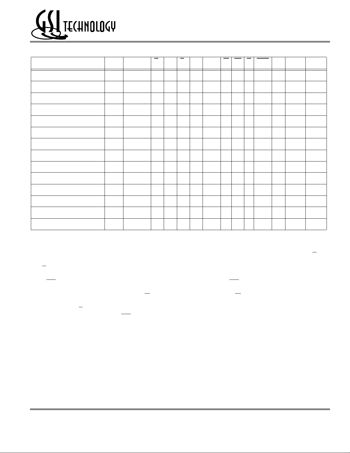
165 Bump BGA—x18 Commom I/O—Top View (Package D)
1234567891011
ANC
BNC
CNCNC
DNC
ENC
FNC
GNC
HFT
J
K
L
DQB NC V
DQB NC V
DQB NC V
A6 E1 BB NC E3
A7 E2 NC BA CK W G A18 A9 NC B
V
DQB V
DQB V
DQB V
DQB V
MCH NC
DDQ
DDQ
DDQ
DDQ
DDQ
DDQ
DDQ
DDQ
CKE
V
SS
V
DD
V
DD
V
DD
V
DD
V
DD
V
DD
V
DD
V
DD
V
SS
V
SS
V
SS
V
SS
V
SS
V
SS
V
SS
V
SS
V
SS
V
SS
V
SS
V
SS
V
SS
V
SS
V
SS
V
SS
V
SS
V
SS
V
V
V
V
V
V
V
V
V
ADV A17 A8
SS
SS
SS
SS
SS
SS
SS
SS
SS
V
SS
V
DD
V
DD
V
DD
V
DD
V
DD
V
DD
V
DD
V
DD
V
V
V
V
V
DDQ
DDQ
DDQ
DDQ
DDQ
NC DQA C
NC DQA D
NC DQA E
NC DQA F
NC DQA G
NC ZQ ZZ H
V
V
V
DDQ
DDQ
DDQ
DQA NC J
DQA NC K
DQA NC L
A19
A
M
N
DQB NC V
DQB DNU V
PNCNC
RLBO
NC A3 A2 TMS A0 TCK A10 A13 A15 A16 R
DDQ
DDQ
A5 A4 TDI A1 TDO A11 A12 A14 NC P
V
DD
V
SS
V
SS
V
SS
V
SS
NC NC NC V
V
DD
SS
V
V
DDQ
DDQ
DQA NC M
NC NC N
11 x 15 Bump BGA—13 mm x 15 mm Body—1.0 mm Bump Pitch
Rev: 2.18a 12/2002 4/38 © 1999, Giga Semiconductor, Inc.
Specifications cited are subject to change without notice. For latest documentation see http://www.gsitechnology.com.
GS8162Z18(B/D)/GS8162Z36(B/D)/GS8162Z72(C)
165 Bump BGA—x36 Common I/O—Top View (Package D)
1234567891011
ANC
BNC
C
D
E
F
G
HFT
J
K
L
DQC NC V
DQC DQC V
DQC DQC V
DQC DQC V
DQC DQC V
MCH NC
DQD DQD V
DQD DQD V
DQD DQD V
A6 E1 BC BB E3 CKE ADV A17 A8
NC
A7 E2 BD BA CK W G A18 A9 NC B
DDQ
DDQ
DDQ
DDQ
DDQ
DDQ
DDQ
DDQ
V
SS
V
DD
V
DD
V
DD
V
DD
V
DD
V
DD
V
DD
V
DD
V
SS
V
SS
V
SS
V
SS
V
SS
V
SS
V
SS
V
SS
V
SS
V
SS
V
SS
V
SS
V
SS
V
SS
V
SS
V
SS
V
SS
V
SS
V
SS
V
SS
V
SS
V
SS
V
SS
V
SS
V
SS
V
SS
V
SS
V
V
V
V
V
V
V
V
V
SS
DD
DD
DD
DD
DD
DD
DD
DD
V
V
V
V
V
DDQ
DDQ
DDQ
DDQ
DDQ
NC DQB C
DQB DQB D
DQB DQB E
DQB DQB F
DQB DQB G
NC ZQ ZZ H
V
V
V
DDQ
DDQ
DDQ
DQA DQA J
DQA DQA K
DQA DQA L
A
M
N
DQD DQD V
DQD DNU V
PNCNC
RLBO
NC A3 A2 TMS A0 TCK A10 A13 A15 A16 R
DDQ
DDQ
A5 A4 TDI A1 TDO A11 A12 A14 NC P
V
DD
V
SS
V
SS
V
SS
V
SS
NC NC NC V
V
DD
SS
V
V
DDQ
DDQ
DQA DQA M
NC DQA N
11 x 15 Bump BGA—13 mm x 15 mm Body—1.0 mm Bump Pitch
Rev: 2.18a 12/2002 5/38 © 1999, Giga Semiconductor, Inc.
Specifications cited are subject to change without notice. For latest documentation see http://www.gsitechnology.com.
GS8162Z36 Pad Out
GS8162Z18(B/D)/GS8162Z36(B/D)/GS8162Z72(C)
119 Bump BGA—Top View (Package B)
1234567
A V
DDQ
B NC E
C NC A
D DQ
E DQ
F V
G
H DQ
J
K DQ
L DQ
DQ
V
C4
C3
DDQ
C2
C1
DDQ
A1
A2
DQ
DQ
DQ
DQ
DQ
V
DQ
DQ
6
A
2
5
C9
C8
C7
C6
C5
DD
A5
A6
7
A
4
A
3
A
V
SS
V
SS
V
SS
C
B
V
SS
NC V
V
SS
D
B
18
A
ADV A
V
DD
ZQ V
1
E
G V
17
A
W V
DD
CK V
NC B
8
A
15
14
A
SS
V
SS
SS
B
B
SS
NC V
SS
A
A
DQ
DQ
DQ
DQ
DQ
DQ
DQ
9
A
E
16
DD
V
DDQ
3
NC
NC
B9
B8
B7
B6
B5
A5
A6
DQ
DQ
V
DQ
DQ
V
DQ
DQ
B4
B3
DDQ
B2
B1
DDQ
A1
A2
M V
N DQ
P DQ
R
T
U V
DDQ
A3
A4
NC A
NC NC A
DDQ
DQ
DQ
DQ
A7
A8
A9
2
V
SS
V
SS
V
SS
LBO V
10
CKE V
1
A
0
A
DD
11
A
SS
V
SS
V
SS
FT A
12
A
A7
DQ
A8
DQ
A9
DQ
13
NC ZZ
TMS TDI TCK TDO NC V
V
DQ
DQ
PE
DDQ
A3
A4
DDQ
Rev: 2.18a 12/2002 6/38 © 1999, Giga Semiconductor, Inc.
Specifications cited are subject to change without notice. For latest documentation see http://www.gsitechnology.com.
GS8162Z18 Pad Out
GS8162Z18(B/D)/GS8162Z36(B/D)/GS8162Z72(C)
119 Bump BGA—Top View (Package B)
1234567
A V
B
C
D DQ
DDQ
NC E
NC A
B1
NC V
E NC DQ
F V
G
H
J V
DDQ
NC DQ
DQ
DDQ
B4
NC V
NC V
V
K NC DQ
L
DQ
B6
NC NC NC B
6
A
2
5
B2
B3
DD
B5
7
A
4
A
3
A
SS
V
SS
SS
B
B
SS
NC V
V
SS
18
A
ADV A
V
DD
ZQ V
1
E
G V
17
A
W V
DD
CK V
8
A
15
14
A
SS
V
SS
SS
9
A
3
E
16
A
PA9
DQ
NC DQ
A7
DQ
V
V
NC NC DQ
A5
DQ
SS
NC V
SS
A
NC DQ
DQ
DD
V
A3
DDQ
NC
NC
NC
A8
DDQ
A6
NC
DDQ
A4
NC
M V
N
DQ
DDQ
B8
P NC DQ
R NC A
T
U
NC A
V
DDQ
B7
DQ
NC V
PB9
2
10
V
SS
SS
V
SS
LBO V
11
A
CKE V
1
A
0
A
DD
NC A
SS
V
SS
V
SS
FT A
12
NC V
A2
DQ
NC DQ
13
19
A
TMS TDI TCK TDO NC V
DDQ
NC
A1
PE
ZZ
DDQ
Rev: 2.18a 12/2002 7/38 © 1999, Giga Semiconductor, Inc.
Specifications cited are subject to change without notice. For latest documentation see http://www.gsitechnology.com.
GS8162Z18(B/D)/GS8162Z36(B/D)/GS8162Z72(C)
GS8162Z18/36 119-Bump and 165-Bump BGA Pin Description
Symbol Type Description
1
A0, A
An I Address Inputs
DQ
A1
A9
–DQ
DQB1–DQ
DQC1–DQ
DQD1–DQ
A
, BB, BC, B
B
B9
C0
D0
D
NC — No Connect
CK I Clock Input Signal; active high
CKE
PE
W
E
1 I Chip Enable; active low
E3
E
2
G
ADV I Burst address counter advance enable; active high
ZZ I Sleep mode control; active high
FT
LBO
ZQ I
TMS
TDI
TDO
TCK
V
DD
V
SS
V
DDQ
I Address field LSBs and Address Counter Preset Inputs
I/O Data Input and Output pins
I Byte Write Enable for DQA, DQB, DQC, DQD I/Os; active low
I Clock Enable; active low
I Parity Bit Enable; active low (High = x16/32 Mode, Low = x18/36 Mode)
I Write Enable; active low
I Chip Enable; active low
I Chip Enable; active high
I Output Enable; active low
I Flow Through or Pipeline mode; active low
I Linear Burst Order mode; active low
FLXDrive Output Impedance Control (Low = Low Impedance [High Drive], High = High Impedance [Low
Drive])
I Scan Test Mode Select
I Scan Test Data In
O Scan Test Data Out
I Scan Test Clock
I Core power supply
I I/O and Core Ground
I Output driver power supply
BPR1999.05.18
Rev: 2.18a 12/2002 8/38 © 1999, Giga Semiconductor, Inc.
Specifications cited are subject to change without notice. For latest documentation see http://www.gsitechnology.com.
GS8162Z18(B/D)/GS8162Z36(B/D)/GS8162Z72(C)
Functional Details
Clocking
Deassertion of the Clock Enable (CKE) input blocks the Clock input from reaching the RAM's internal circuits. It may be used to
suspend RAM operations. Failure to observe Clock Enable set-up or hold requirements will result in erratic operation.
Pipeline Mode Read and Write Operations
All inputs (with the exception of Output Enable, Linear Burst Order and Sleep) are synchronized to rising clock edges. Single cycle
read and write operations must be initiated with the Advance/Load
activation is accomplished by asserting all three of the Chip Enable inputs (E
inputs will deactivate the device.
pin (ADV) held low, in order to load the new address. Device
, E2, and E3). Deassertion of any one of the Enable
1
Function W
B
B
A
B
B
B
C
D
Read H X X X X
Write Byte “a” L L H H H
Write Byte “b” L H L H H
Write Byte “c” L H H L H
Write Byte “d” L H H H L
Write all Bytes L L L L L
Write Abort/NOP L H H H H
Read operation is initiated when the following conditions are satisfied at the rising edge of clock: CKE
chip enables (E
1
, E2, and E3) are active, the write enable input signals W is deasserted high, and ADV is asserted low. The address
is asserted low, all three
presented to the address inputs is latched into the address register and presented to the memory core and control logic. The control
logic determines that a read access is in progress and allows the requested data to propagate to the input of the output register. At
the next rising edge of clock the read data is allowed to propagate through the output register and onto the output pins.
Write operation occurs when the RAM is selected, CKE is active, and the Write input is sampled low at the rising edge of clock.
The Byte Write Enable inputs (B
, BB, BC, and BD) determine which bytes will be written. All or none may be activated. A write
A
cycle with no Byte Write inputs active is a no-op cycle. The pipelined NBT SRAM provides double late write functionality,
matching the write command versus data pipeline length (2 cycles) to the read command versus data pipeline length (2 cycles). At
the first rising edge of clock, Enable, Write, Byte Write(s), and Address are registered. The Data In associated with that address is
required at the third rising edge of clock.
Flow Through Mode Read and Write Operations
Operation of the RAM in Flow Through mode is very similar to operations in Pipeline mode. Activation of a Read Cycle and the
use of the Burst Address Counter is identical. In Flow Through mode the device may begin driving out new data immediately after
new address are clocked into the RAM, rather than holding new data until the following (second) clock edge. Therefore, in Flow
Through mode the read pipeline is one cycle shorter than in Pipeline mode.
Write operations are initiated in the same way, but differ in that the write pipeline is one cycle shorter as well, preserving the ability
to turn the bus from reads to writes without inserting any dead cycles. While the pipelined NBT RAMs implement a double late
write protocol in Flow Through mode a single late write protocol mode is observed. Therefore, in Flow Through mode, address
and control are registered on the first rising edge of clock and data in is required at the data input pins at the second rising edge of
clock.
Rev: 2.18a 12/2002 9/38 © 1999, Giga Semiconductor, Inc.
Specifications cited are subject to change without notice. For latest documentation see http://www.gsitechnology.com.
GS8162Z18(B/D)/GS8162Z36(B/D)/GS8162Z72(C)
Synchronous Truth Table
Operation Type Address E1E2E3ZZ ADV W Bx G CKE CK DQ Notes
Deselect Cycle, Power Down D None H X X L L X X X L L-H High-Z
Deselect Cycle, Power Down D None X X H L L X X X L L-H High-Z
Deselect Cycle, Power Down D None X L X L L X X X L L-H High-Z
Deselect Cycle, Continue D None X X X L H X X X L L-H High-Z 1
Read Cycle, Begin Burst R External L H L L L H X L L L-H Q
Read Cycle, Continue Burst B Next X X X L H X X L L L-H Q 1,10
NOP/Read, Begin Burst R External L H L L L H X H L L-H High-Z 2
Dummy Read, Continue Burst B Next X X X L H X X H L L-H High-Z 1,2,10
Write Cycle, Begin Burst W External L H L L L L L X L L-H D 3
Write Cycle, Continue Burst B Next X X X L H X L X L L-H D 1,3,10
NOP/Write Abort, Begin Burst W None L H L L L L H X L L-H High-Z 2,3
Write Abort, Continue Burst B Next X X X L H X H X L L-H High-Z 1,2,3,10
Clock Edge Ignore, Stall Current X X X L X X X X H L-H - 4
Sleep Mode None X X X H X X X X X X High-Z
Notes:
1. Continue Burst cycles, whether Read or Write, use the same control inputs. A Deselect continue cycle can only be entered into if a
Deselect cycle is executed first.
2. Dummy Read and Write abort can be considered NOPs because the SRAM performs no operation. A Write abort occurs when the W
is sampled low but no Byte Write pins are active, so no write operation is performed.
3. G
can be wired low to minimize the number of control signals provided to the SRAM. Output drivers will automatically turn off during write
cycles.
4. If CKE
5. X = Don’t Care; H = Logic High; L = Logic Low; Bx
6. All inputs, except G
7. Wait states can be inserted by setting CKE
8. This device contains circuitry that ensures all outputs are in High Z during power-up.
9. A 2-bit burst counter is incorporated.
10. The address counter is incriminated for all Burst continue cycles.
High occurs during a pipelined read cycle, the DQ bus will remain active (Low Z). If CKE High occurs during a write cycle, the bus
will remain in High Z.
= High = All Byte Write signals are high; Bx = Low = One or more Byte/Write signals
are Low
and ZZ must meet setup and hold times of rising clock edge.
high.
pin
Rev: 2.18a 12/2002 10/38 © 1999, Giga Semiconductor, Inc.
Specifications cited are subject to change without notice. For latest documentation see http://www.gsitechnology.com.
GS8162Z18(B/D)/GS8162Z36(B/D)/GS8162Z72(C)
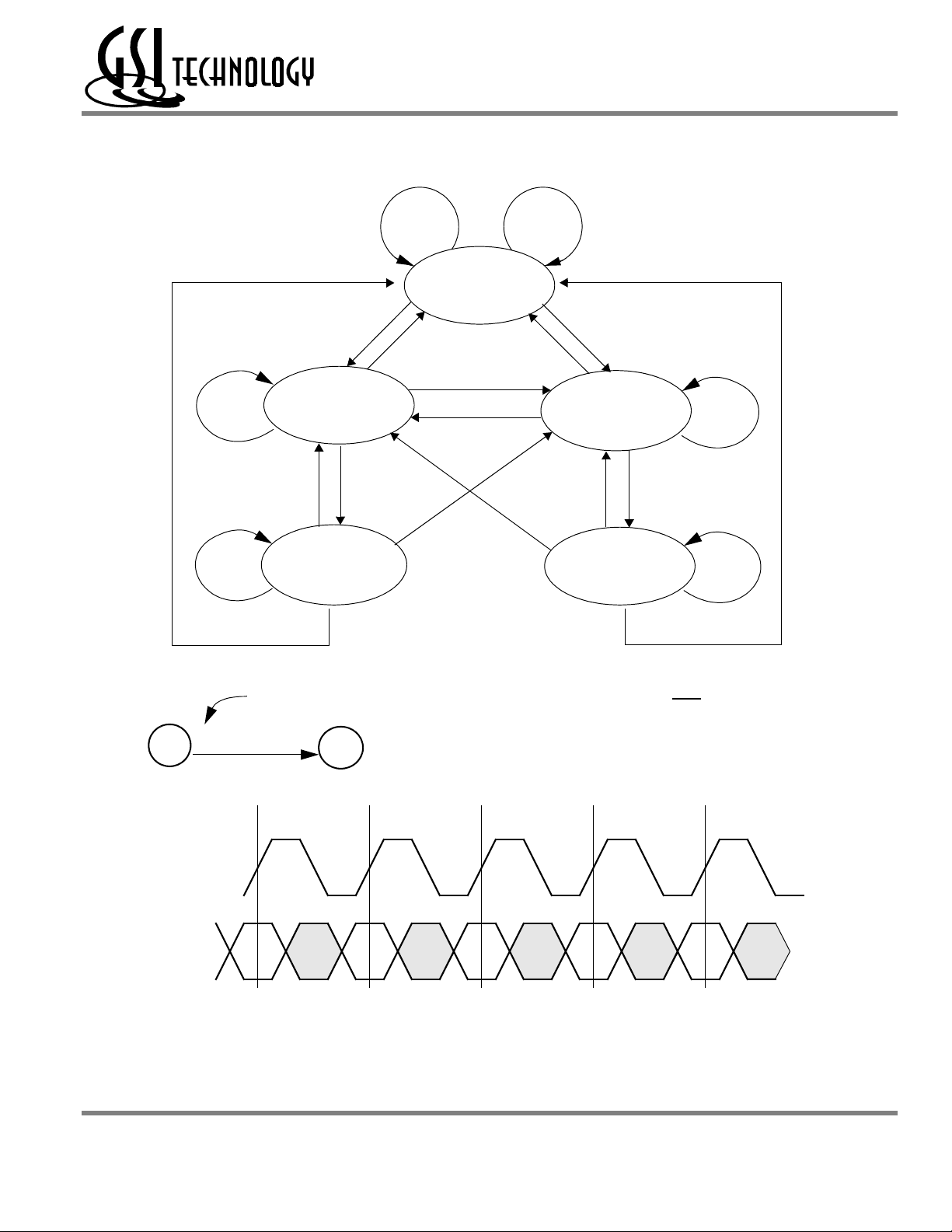
Pipelined and Flow Through Read Write Control State Diagram
D
B
Deselect
R
D
W
New Read New Write
R
B
R
W
W
R
R
Burst Read Burst Write
B
Key Notes
ƒ
Current State (n)
Input Command Code
Transition
Next State (n+1)
1. The Hold command (CKE Low) is not
shown because it prevents any state change.
2. W, R, B, and D represent input command
codes as indicated in the Synchronous Truth Table.
D
W
B
W
B
DD
n n+1 n+2 n+3
Clock (CK)
Command
Current State Next State
ƒ
ƒƒƒ
Current State and Next State Definition for Pipelined and Flow through Read/Write Control State Diagram
Rev: 2.18a 12/2002 11/38 © 1999, Giga Semiconductor, Inc.
Specifications cited are subject to change without notice. For latest documentation see http://www.gsitechnology.com.
GS8162Z18(B/D)/GS8162Z36(B/D)/GS8162Z72(C)
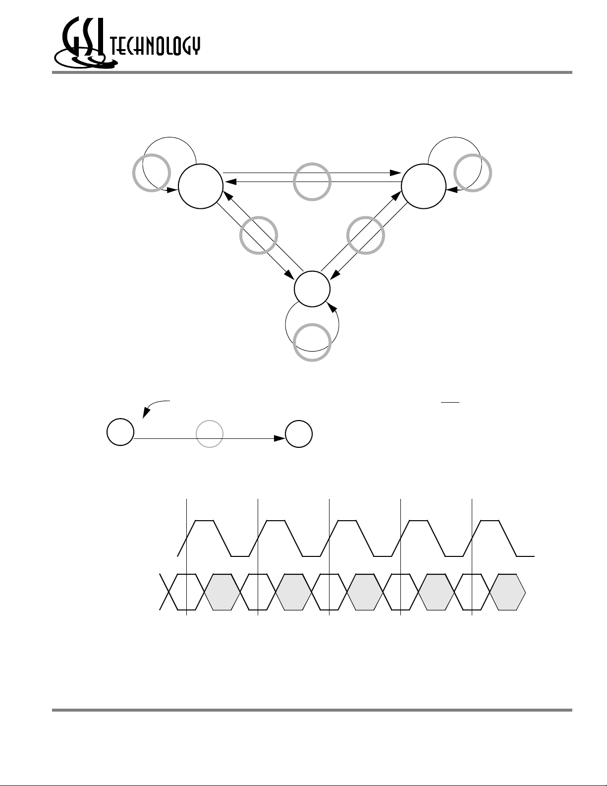
Pipeline Mode Data I/O State Diagram
Intermediate Intermediate
Key
ƒ
Transition
Current State (n) Next State (n+2)
W
B
High Z
(Data In)
Input Command Code
R
D
Intermediate
Transition
Intermediate State (N+1)
Intermediate
W
High Z
B
D
Intermediate
R
B
Data Out
W
(Q Valid)
Intermediate
R
D
Notes
1. The Hold command (CKE Low) is not
shown because it prevents any state change.
2. W, R, B, and D represent input command
codes as indicated in the Truth Tables.
n n+1 n+2 n+3
Clock (CK)
Command
Current State
ƒ
ƒƒƒ
Intermediate
Next State
State
Current State and Next State Definition for Pipeline Mode Data I/O State Diagram
Rev: 2.18a 12/2002 12/38 © 1999, Giga Semiconductor, Inc.
Specifications cited are subject to change without notice. For latest documentation see http://www.gsitechnology.com.
 Loading...