

GSI GS78116B-15I, GS78116B-12I, GS78116B-12, GS78116B-10I, GS78116B-10 Datasheet
...
GS78116B
BGA
512K x 16
Commercial Temp
Industrial Temp
8Mb Asynchronous SRAM
Features
• Fast access time: 10, 12, 15 ns
• CMOS low power operation: 300/250/220/180 mA at
minimum cycle time
• Single 3.3 V ± 0.3 V power supply
• All inputs and outputs are TTL-compatible
• Fully static operation
• Industrial Temperature Option: –40° to 85°C
• 14 mm x 22 mm, 119-Bump, 1.27 mm Pitch Ball Grid Array
package
Description
The GS78116 is a high speed CMOS static RAM organized as
524,288-words by 16-bits. Static design eliminates the need for
external clocks or timing strobes. The GS78116 operates on a
single 3.3 V power supply and all inputs and outputs are TTLcompatible. The GS78116 is available in 14 mm x 22 mm
BGA package.
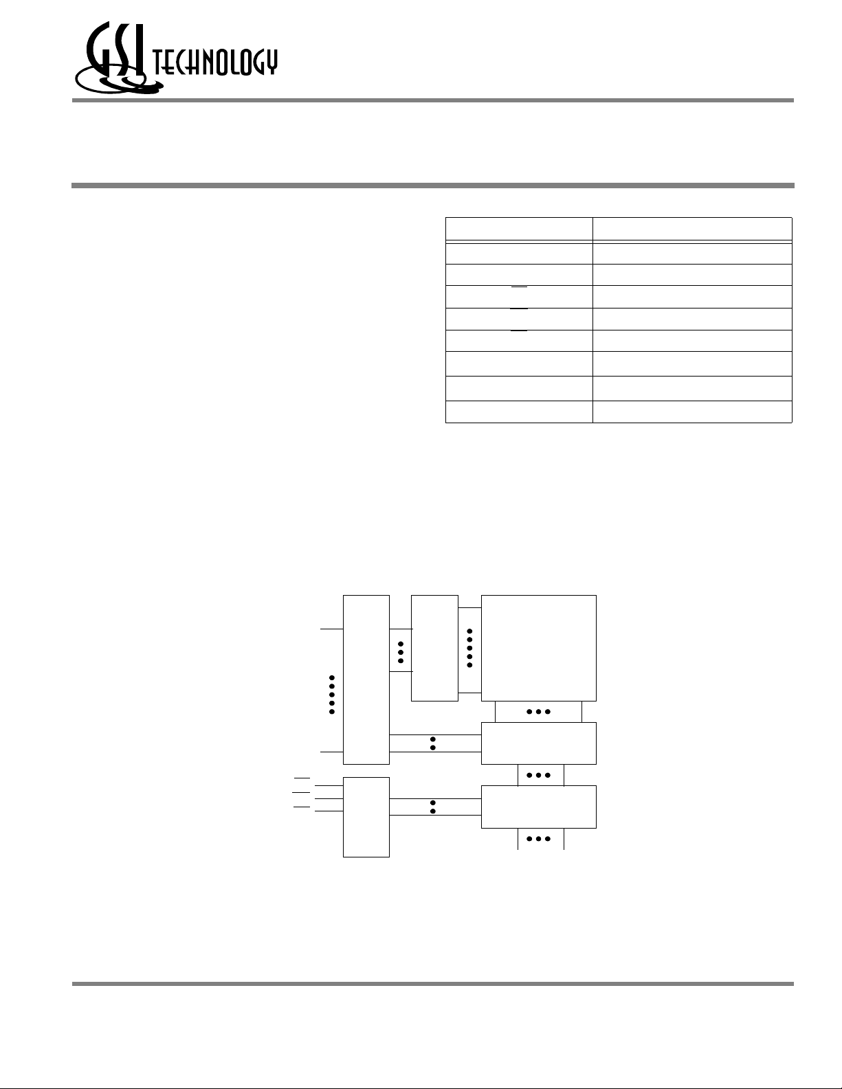
Pin Descriptions
Symbol Description
A0 to A18 Address input
DQ1 to DQ16 Data input/output
CE Chip enable input
WE Write enable input
OE Output enable input
V
DD
V
SS
NC No connect
10, 12, 15 ns
3.3 V V
+3.3 V power supply
Ground
DD
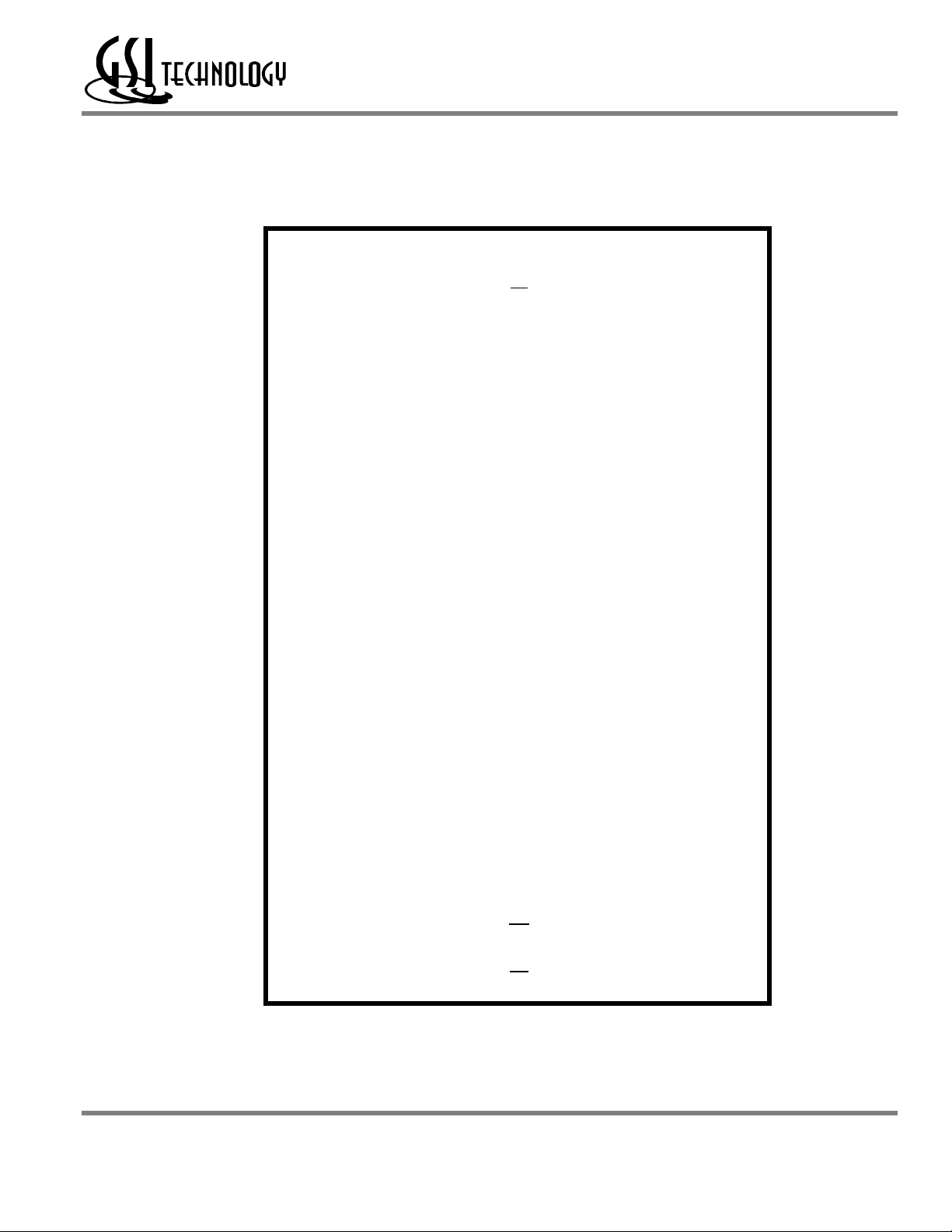
Block Diagram
A0
A18
CE
WE
OE
Address
Input
Buffer
Control
Row
Decoder
Memory Array
Column
Decoder
I/O Buffer
DQ1
DQ16
Rev: 1.02 9/2001 1/11 © 1999, Giga Semiconductor, Inc.
For latest documentation see http://www.gsitechnology.com.
512K x 16 Async SRAM in 119-Bump, 14 mm x 22 mm
Top View
1 2 3 4 5 6 7
A NC A15 A14 A16 A13 A12 NC
GS78116B
B
NC,
VSS
A11 A10 CE A9 A8 NC
C NC NC
D NC
V
DD
E DQ1 NC
F DQ2
V
DD
G DQ3 NC
H DQ4
J VDD
K DQ5
V
DD
V
SS
V
DD
L DQ6 NC
VDD,
NC
V
SS
V
DD
V
SS
V
DD
V
SS
V
DD
V
SS
V
DD
A17
V
V
V
V
V
V
V
V
SS
SS
SS
SS
SS
SS
SS
SS
VSS,
NC
V
SS
V
DD
V
SS
V
DD
V
SS
V
DD
V
SS
V
DD
NC NC
V
DD
NC
NC DQ16
V
DD
DQ15
NC DQ14
V
V
V
DD
SS
DD
DQ13
VDD
DQ12
NC DQ11
M DQ7
V
N DQ8 NC
P NC
V
DD
DD
V
SS
V
DD
V
SS
V
SS
V
SS
V
SS
V
SS
V
DD
V
SS
V
DD
DQ10
NC DQ9
V
DD
NC
R NC NC NC A18 NC NC NC
T NC A7 A6 WE A5 A4
NC,
VSS
U NC A3 A2 OE A1 A0 NC
Note: Bumps 1B, 7T, 3C, and 5C are actually NC’s but should be wired 3C = VDD and 1B, 7T and 5C = VSS to assure compatibility
with future versions.
Rev: 1.02 9/2001 2/11 © 1999, Giga Semiconductor, Inc.
For latest documentation see http://www.gsitechnology.com.
Truth Table
CE OE WE DQ1 to DQ8 VDD Current
H X X Not Selected ISB1, ISB2
L L H Read
L X L Write IDD
L H H High Z
Note: X: “H” or “L”
Absolute Maximum Ratings
Parameter Symbol Rating Unit
Supply Voltage VDD –0.5 to +4.6 V
GS78116B
Input Voltage
Output Voltage
V
V
OUT
IN
(≤ 4.6 V max.)
–0.5 to VDD+0.5
(≤ 4.6 V max.)
–0.5 to V
DD
+0.5
V
V
Allowable power dissipation PD 1.5 W
Storage temperature
T
STG
–55 to 150
o
C
Note:
Permanent device damage may occur if Absolute Maximum Ratings are exceeded. Functional operation shall be restricted to Recommended
Operating Conditions. Exposure to higher than recommended voltages for extended periods of time could affect device reliability.
Recommended Operating Conditions
Parameter Symbol Min Typ Max Unit
Supply Voltage for -10/12/15
Input High Voltage
Input Low Voltage
Ambient Temperature,
Commercial Range
V
DD
V
IH
V
IL
T
Ac
3.0 3.3 3.6 V
2.0 —
VDD +0.3
–0.3 — 0.8 V
0 — 70
V
o
C
Ambient Temperature,
Industrial Range
T
Ai
–40 — 85
o
C
Notes:
1. Input overshoot voltage should be less than VDD +2 V and not exceed 20 ns.
2. Input undershoot voltage should be greater than –2 V and not exceed 20 ns.
Rev: 1.02 9/2001 3/11 © 1999, Giga Semiconductor, Inc.
For latest documentation see http://www.gsitechnology.com.
Capacitance
GS78116B
Parameter Symbol
Input Capacitance
Output Capacitance
C
IN
C
OUT
Test
Condition
V
= 0 V
IN
V
= 0 V
OUT
Max Unit
10 pF
7 pF
Notes:
1. Tested at TA = 25°C, f = 1 MHz
2. These parameters are sampled and are not 100% tested.
DC I/O Pin Characteristics
Parameter Symbol Test Conditions Min Max
Input Leakage
Current
Output Leakage
Current
Output High Voltage
Output Low Voltage
I
IL
I
OL
V
OH
V
OL
V
= 0 to VDD
IN
Output High Z,
V
= 0 to VDD
OUT
I
= –4 mA
OH
I
= +4 mA
OL
–2 uA 2 uA
–1 uA 1 uA
2.4
0.4 V
Power Supply Currents
Parameter Symbol Test Conditions
E ≤ V
Operating
Supply
Current
Standby
Current
Standby
Current
I
I
I
DD
SB1
SB2
All other inputs
≥ VIH or ≤ V
Min. cycle time
I
OUT
E ≥ VIH
All other inputs
≥ VIH or ≤V
Min. cycle time
E ≥ VDD – 0.2V
All other inputs
≥ VDD – 0.2 V or ≤ 0.2 V
IL
= 0 mA
0 to 70°C –40 to 85°C
10 ns 12 ns 15 ns 10 ns 12 ns 15 ns
IL
IL
225 mA 220 mA 180 mA 270 mA 240 mA 200 mA
130 mA 120 mA 110 mA 150 mA 140 mA 130 mA
60 mA 80 mA
Rev: 1.02 9/2001 4/11 © 1999, Giga Semiconductor, Inc.
For latest documentation see http://www.gsitechnology.com.
 Loading...