

GSI GS74117AX-8I, GS74117AX-8, GS74117AX-7I, GS74117AX-7, GS74117AX-12I Datasheet
...
GS74117AX
FP-BGA
256K x 16
Commercial Temp
Industrial Temp
4Mb Asynchronous SRAM
Features
• Fast access time: 7, 8, 10, 12 ns
• CMOS low power operation: 150/130/105/95 mA at
minimum cycle time
• Single 3.3 V power supply
• All inputs and outputs are TTL-compatible
• Byte control
• Fully static operation
• Industrial Temperature Option: –40° to 85°C
• Package:
X: 6 mm x 10 mm Fine Pitch Ball Grid Array
package
Description
The GS74117A is a high speed CMOS Static RAM organized
as 262,144 words by 16 bits. Static design eliminates the need
for external clocks or timing strobes. The GS operates on a
single 3.3 V power supply and all inputs and outputs are TTLcompatible. The GS74117A is available in a 6 x 10 mm Fine
Pitch BGA package.
Pin Descriptions
7, 8, 10, 12 ns
3.3 V V
Center VDD and V
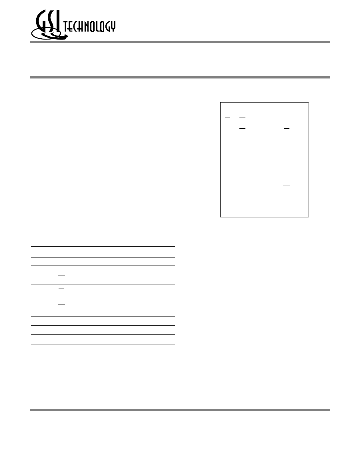
Fine Pitch BGA 256K x 16 Bump Configuration
123456
0
ALB
BDQ1UB A
CDQ3DQ2A
DVSSDQ4A
EVDDDQ5NC A16DQ12V
FDQ6DQ7A
GDQ8NC A
HNCA12A
OE A
Package X
6 x 10 mm Bump Pitch
Top View
1
A
A2NC
3
A4CE DQ
5
A6DQ15DQ
17
A7DQ13V
8
A9DQ10DQ
10A11
13A14A15
WE DQ
16
14
DD
SS
11
9
NC
DD
SS
Symbol Description
17
A0–A
DQ
1–DQ16 Data input/output
CE
LB
UB
WE
OE
V
DD
V
SS
NC No connect
Rev: 1.02 10/2002 1/12 © 2001, Giga Semiconductor, Inc.
Specifications cited are subject to change without notice. For latest documentation see http://www.gsitechnology.com.
Address input
Chip enable input
Lower byte enable input
(DQ1 to DQ8)
Upper byte enable input
(DQ9 to DQ16)
Write enable input
Output enable input
+3.3 V power supply
Ground
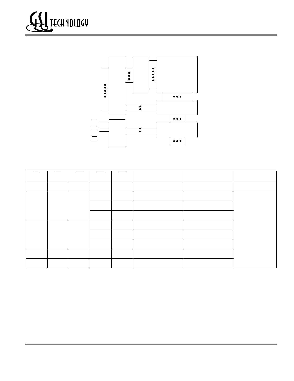
Block Diagram
Truth Table
A
A
CE
WE
OE
UB
LB
0
17
_____
_____
Address
Input
Buffer
Control
Row
Decoder
Memory Array
Column
Decoder
I/O Buffer
DQ
1
DQ
GS74117AX
16
CE OE WE LB UB DQ1 to DQ
H X X X X Not Selected Not Selected ISB1, ISB
L L Read Read
LLH
LXL
L H H X X High Z High Z
L X X H H High Z High Z
Note: X: “H” or “L”
L H Read High Z
H L High Z Read
LL Write Write
L H Write Not Write, High Z
H L Not Write, High Z Write
8
DQ9 to DQ
16
VDD Current
2
DD
I
Rev: 1.02 10/2002 2/12 © 2001, Giga Semiconductor, Inc.
Specifications cited are subject to change without notice. For latest documentation see http://www.gsitechnology.com.
Absolute Maximum Ratings
Parameter Symbol Rating Unit
GS74117AX
Supply Voltage V
Input Voltage V
Output Voltage V
DD
IN
OUT
–0.5 to +4.6 V
–0.5 to V
DD
+0.5
(≤ 4.6 V max.)
–0.5 to V
DD
+0.5
(≤ 4.6 V max.)
V
V
Allowable power dissipation PD 0.7 W
Storage temperature T
STG
–55 to 150
o
C
Note:
Permanent device damage may occur if Absolute Maximum Ratings are exceeded. Functional operation shall be restricted to Recommended Operating Conditions. Exposure to higher than recommended voltages for extended periods of time could affect device
reliability.
Recommended Operating Conditions
Parameter Symbol Min Typ Max Unit
Supply Voltage for -7/-8/-10/-12
Input High Voltage V
Input Low Voltage V
V
DD
IH
IL
3.0 3.3 3.6 V
V
2.0 —
DD
+0.3
–0.3 — 0.8 V
V
Ambient Temperature,
Commercial Range
Ambient Temperature,
Industrial Range
Ac 0—70
T
T
I
A
–40 — 85
o
C
o
C
Notes:
1. Input overshoot voltage should be less than V
+2 V and not exceed 20 ns.
DD
2. Input undershoot voltage should be greater than –2 V and not exceed 20 ns.
Rev: 1.02 10/2002 3/12 © 2001, Giga Semiconductor, Inc.
Specifications cited are subject to change without notice. For latest documentation see http://www.gsitechnology.com.
GS74117AX
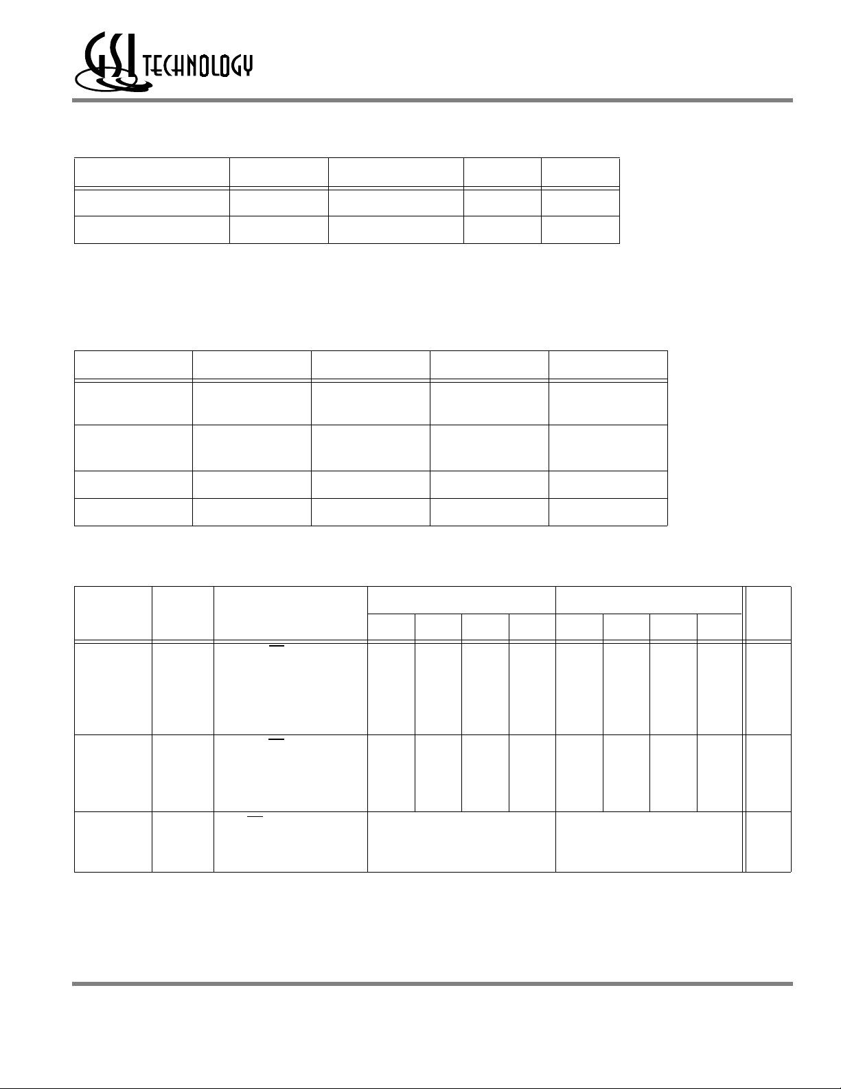
Capacitance
Parameter Symbol Test Condition Max Unit
Input Capacitance C
Output Capacitance C
IN
OUT VOUT = 0 V 7 pF
Notes:
A
1. Tested at T
= 25°C, f = 1 MHz
2. These parameters are sampled and are not 100% tested.
IN
V
= 0 V 5 pF
DC I/O Pin Characteristics
Parameter Symbol Test Conditions Min Max
Input Leakage
Current
Output Leakage
Current
Output High Voltage V
Output Low Voltage V
I
IL
I
LO
OH IOH = –4 mA 2.4 —
OL
IN
V
= 0 to V
DD
Output High Z
V
OUT
= 0 to V
LO
I
DD
= +4 mA — 0.4 V
– 1 uA 1 uA
–1 uA 1 uA
Power Supply Currents
Parameter Symbol Test Conditions
CE ≤ VIL
Operating
Supply
Current
Standby
Current
Standby
Current
I
I
I
SB1
SB2
DD
All other inputs
≥ V
IH or ≤ VIL
Min. cycle time
I
OUT = 0 mA
CE ≥ V
All other inputs
≥ V
IH
or ≤V
Min. cycle time
CE ≥ VDD – 0.2 V
All other inputs
≥ V
DD – 0.2 V or ≤ 0.2 V
0 to 70°C –40 to 85°C
Unit
7 ns 8 ns 10 ns 12 ns 7 ns 8 ns 10 ns 12 ns
150 130 105 90 160 140 115 100 mA
IH
IL
28 30 25 22 38 40 35 32 mA
10 20 mA
Rev: 1.02 10/2002 4/12 © 2001, Giga Semiconductor, Inc.
Specifications cited are subject to change without notice. For latest documentation see http://www.gsitechnology.com.
 Loading...