

GSI GS74116J-15, GS74116J-12I, GS74116J-12, GS74116J-10I, GS74116J-10 Datasheet
...
Rev: 2.02 3/2000 1/14 © 1999, Giga Semiconductor, Inc.
Specifications cited are subject to change without notice. For latest documentation see http://www.gsitechnology.com. N
GS74116TP/J/U
256K x 16
4Mb Asynchronous SRAM
8, 10, 12, 15ns
3.3V VDD
Center VDD & VSS
SOJ, TSOP, FP-BGA
Commercial Temp
Industrial Temp
Features
• Fast access time: 8, 10, 12, 15ns
• CMOS low power operation: 170/145/130/110 mA at min.cycle time.
• Single 3.3V ± 0.3V power supply
• All inputs and outputs are TTL compatible
• Byte control
• Fully static operation
• Industrial Temperature Option: -40° to 85°C
• Package line up
J: 400mil, 44 pin SOJ package
TP: 400mil, 44 pin TSOP Type II package
U: 7.20mm x 11.65mm Fine Pitch Ball Grid Array package
Description
The GS74116 is a high speed CMOS static RAM organized as
262,144-words by 16-bits. Static design eliminates the need for external clocks or timing strobes. Operating on a single 3.3V power supply
and all inputs and outputs are TTL compatible. The GS74116 is available in a 7.2x11.65 mm Fine Pitch BGA package, 400 mil SOJ and
400 mil TSOP Type-II packages.
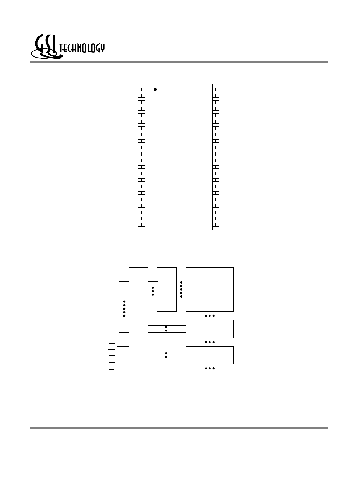
Pin Descriptions
SOJ 256K x 16 Pin Configuration
Fine Pitch BGA 256K x 16 Bump Configuration
7.2x11.65mm 0.75mm Bump Pitch
Top View
Symbol Description
A0 to A17
Address input
DQ1 to DQ16 Data input/output
CE Chip enable input
LB
Lower byte enable input
(DQ1 to DQ8)
UB
Upper byte enable input
(DQ9 to DQ16)
WE Write enable input
OE Output enable input
VDD +3.3V power supply
VSS Ground
NC No connect
1 2 3 4 5 6
A LB OE A0 A1 A2 NC
B DQ16 UB A3 A4 CE DQ1
C DQ14 DQ15 A5 A6 DQ2 DQ3
D VSS DQ13 A17 A7 DQ4 VDD
E VDD DQ12 NC A16 DQ5 VSS
F DQ11 DQ10 A8 A9 DQ7 DQ6
G DQ9 NC A10 A11 WE DQ8
H NC A12 A13 A14 A15 NC
44
43
42
41
40
39
38
37
36
35
34
33
32
31
30
29
28
27
26
25
1
2
3
4
5
6
7
8
9
10
11
12
13
14
15
16
17
18
19
20
A4
A3
A2
A1
A0
CE
DQ1
DQ2
DQ3
DQ4
VDD
VSS
DQ5
DQ6
DQ7
DQ8
WE
A15
A14
A13
A5
A6
A7
OE
UB
LB
DQ16
DQ15
DQ14
DQ13
VSS
VDD
DQ12
DQ11
DQ10
DQ9
NC
A8
A9
A10
Top view
21
22
24
23
A12
A11
44 pin
SOJ
A17A16
Rev: 2.02 3/2000 2/14 © 1999, Giga Semiconductor, Inc.
Specifications cited are subject to change without notice. For latest documentation see http://www.gsitechnology.com. N
GS74116TP/J/U
TSOP-II 256K x 16 Pin Configuration
44
43
42
41
40
39
38
37
36
35
34
33
32
31
30
29
28
27
26
25
1
2
3
4
5
6
7
8
9
10
11
12
13
14
15
16
17
18
19
20
A4
A3
A2
A1
A0
CE
DQ1
DQ2
DQ3
DQ4
VDD
VSS
DQ5
DQ6
DQ7
DQ8
WE
A15
A14
A13
A5
A6
A7
OE
UB
LB
DQ16
DQ15
DQ14
DQ13
VSS
VDD
DQ12
DQ11
DQ10
DQ9
NC
A8
A9
A10
Top view
21
22
24
23
A12
A11
44 pin
TSOP II
A17A16
Memory Array
Row
Decoder
Column
Decoder
Address
Input
Buffer
Control
I/O Buffer
A0
CE
WE
OE
DQ1
A17
Block Diagram
DQ16
UB
_____
LB
_____
Rev: 2.02 3/2000 3/14 © 1999, Giga Semiconductor, Inc.
Specifications cited are subject to change without notice. For latest documentation see http://www.gsitechnology.com. N
GS74116TP/J/U
Note: X: “H” or “L”
Note:
Permanent device damage may occur if Absolute Maximum Ratings are exceeded. Functional operation shall be restricted to Recommended
Operating Conditions. Exposure to higher than recommended voltages for extended periods of time could affect device reliability.
Truth Table
CE OE WE LB UB DQ1 to DQ8 DQ9 to DQ16 VDD Current
H X X X X Not Selected Not Selected ISB1, ISB2
L L H
L L Read Read
IDD
L H Read High Z
H L High Z Read
L X L
L L Write Write
L H Write Not Write, High Z
H L Not Write, High Z Write
L H H X X High Z High Z
L X X H H High Z High Z
Absolute Maximum Ratings
Parameter Symbol Rating Unit
Supply Voltage VDD -0.5 to +4.6 V
Input Voltage VIN
-0.5 to VDD+0.5
(≤ 4.6V max.)
V
Output Voltage VOUT
-0.5 to VDD+0.5
(≤ 4.6V max.)
V
Allowable power dissipation PD 0.7 W
Storage temperature TSTG -55 to 150
o
C
Rev: 2.02 3/2000 4/14 © 1999, Giga Semiconductor, Inc.
Specifications cited are subject to change without notice. For latest documentation see http://www.gsitechnology.com. N
GS74116TP/J/U
Note:
1. Input overshoot voltage should be less than VDD+2V and not exceed 20ns.
2. Input undershoot voltage should be greater than -2V and not exceed 20ns.
Notes:
1. Tested at TA=25°C, f=1MHz
2. These parameters are sampled and are not 100% tested
Recommended Operating Conditions
Parameter Symbol Min Typ Max Unit
Supply Voltage for -10/12/15 VDD 3.0 3.3 3.6 V
Supply Voltage for -8 VDD 3.135 3.3 3.6 V
Input High Voltage VIH 2.0 - VDD+0.3 V
Input Low Voltage VIL -0.3 - 0.8 V
Ambient Temperature,
Commercial Range
TAc 0 - 70
o
C
Ambient Temperature,
Industrial Range
TAI -40 - 85
o
C
Capacitance
Parameter Symbol Test Condition Max Unit
Input Capacitance CIN VIN=0V 5 pF
Output Capacitance COUT VOUT=0V 7 pF
DC I/O Pin Characteristics
Parameter Symbol Test Conditions Min Max
Input Leakage
Current
IIL VIN = 0 to VDD -1uA 1uA
Output Leakage
Current
ILO
Output High Z
VOUT = 0 to VDD
-1uA 1uA
Output High Voltage VOH IOH = - 4mA 2.4
Output Low Voltage VOL ILO = + 4mA 0.4V
Rev: 2.02 3/2000 5/14 © 1999, Giga Semiconductor, Inc.
Specifications cited are subject to change without notice. For latest documentation see http://www.gsitechnology.com. N
GS74116TP/J/U
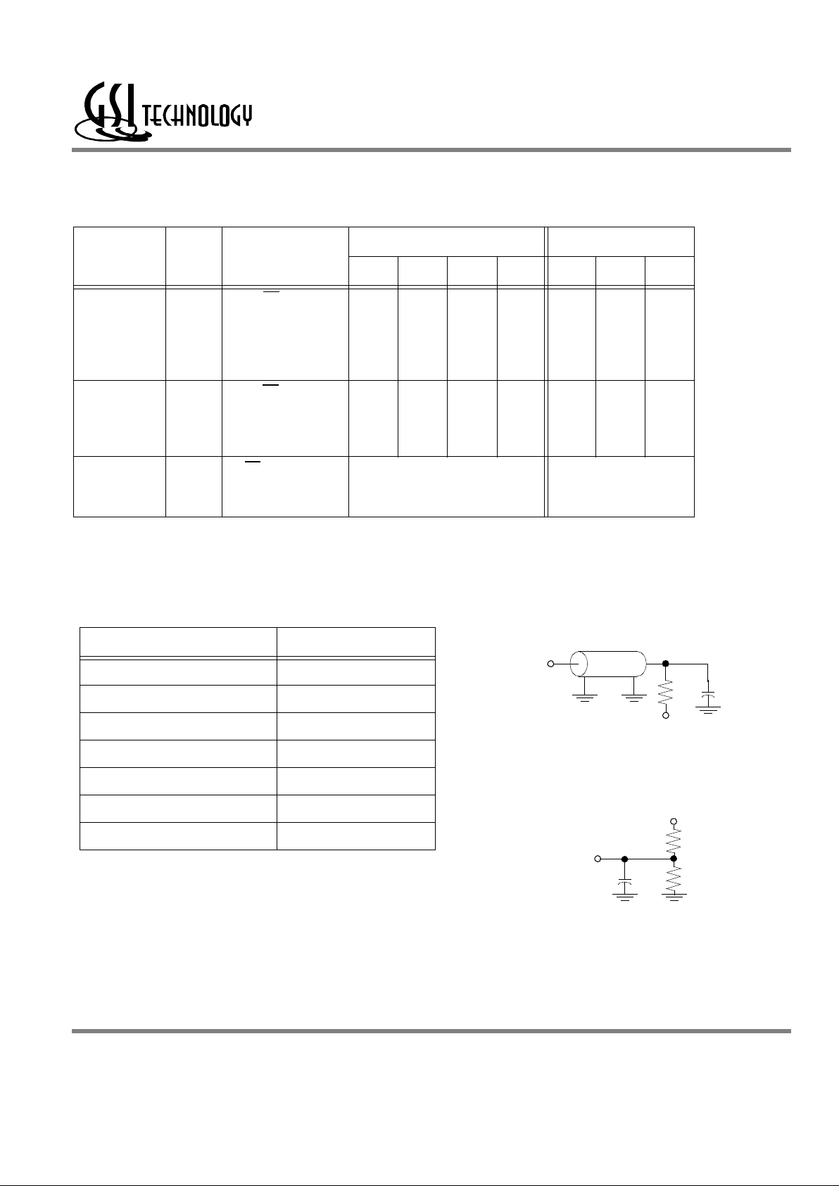
AC Test Conditions
Power Supply Currents
Parameter Symbol Test Conditions
0 to 70°C -40 to 85°C
8ns 10ns 12ns 15ns 10ns 12ns 15ns
Operating
Supply
Current
IDD
CE ≤ VIL
All other inputs
≥ VIH or ≤ VIL
Min. cycle time
IOUT = 0 mA
170mA 145mA 130mA 110mA 155mA 140mA 120mA
Standby
Current
ISB1
CE ≥ VIH
All other inputs
≥ VIH or ≤VIL
Min. cycle time
70mA 65mA 60mA 55mA 75mA 70mA 65mA
Standby
Current
ISB2
CE ≥ VDD - 0.2V
All other inputs
≥ VDD - 0.2V or ≤ 0.2V
30mA 40mA
DQ
VT=1.4V
50Ω
30pF
1
DQ
3.3V
Output Load 1
Output Load 2
589Ω
434Ω
5pF
1
Note:
1. Include scope and jig capacitance.
2. Test conditions as specified with output loading as shown in Fig. 1
unless otherwise noted
3. Output load 2 for tLZ, tHZ, tOLZ and tOHZ.
Parameter Conditions
Input high level VIH=2.4V
Input low level VIL=0.4V
Input rise time tr=1V/ns
Input fall time tf=1V/ns
Input reference level 1.4V
Output reference level 1.4V
Output load Fig. 1& 2
 Loading...