

GS GSM9107ZF Schematic [ru]
30V P-Channel Enhancement Mode MOSFET
Product Description Features
GSM9107, P-Channel enhancement mode
MOSFET, uses Advanced Trench Technology to
provide excellent R
These devices are particularly suited for low
voltage power management, and low in-line power
loss are needed in commercial industrial surface
mount applications.
, low gate charge.
DS(ON)
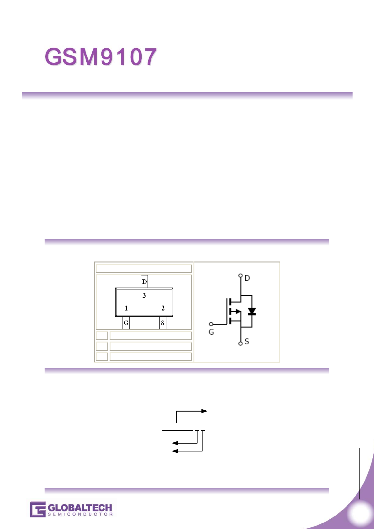
Packages & Pin Assignments
GSM9107ZF (SOT-23-3L)
-30V/-4.0A,R
-30V/-3.2A,R
-30V/-1.0A,R
Super high density cell design for extremely
low R
DS (ON)
SOT-23-3L package design
=65m@VGS=-10.0V
DS(ON)
=80m@VGS=-4.5V
DS(ON)
=105m@VGS=-2.5V
DS(ON)
Applications
Power Management in Note book
LED Display
DC-DC System
LCD Panel
1
2
3
Ordering Information
Gate
Source
Drain
GSM9107
Package Code
Pb Free
GS P/N
Z F
GSM9107
www.gs-power.com
1
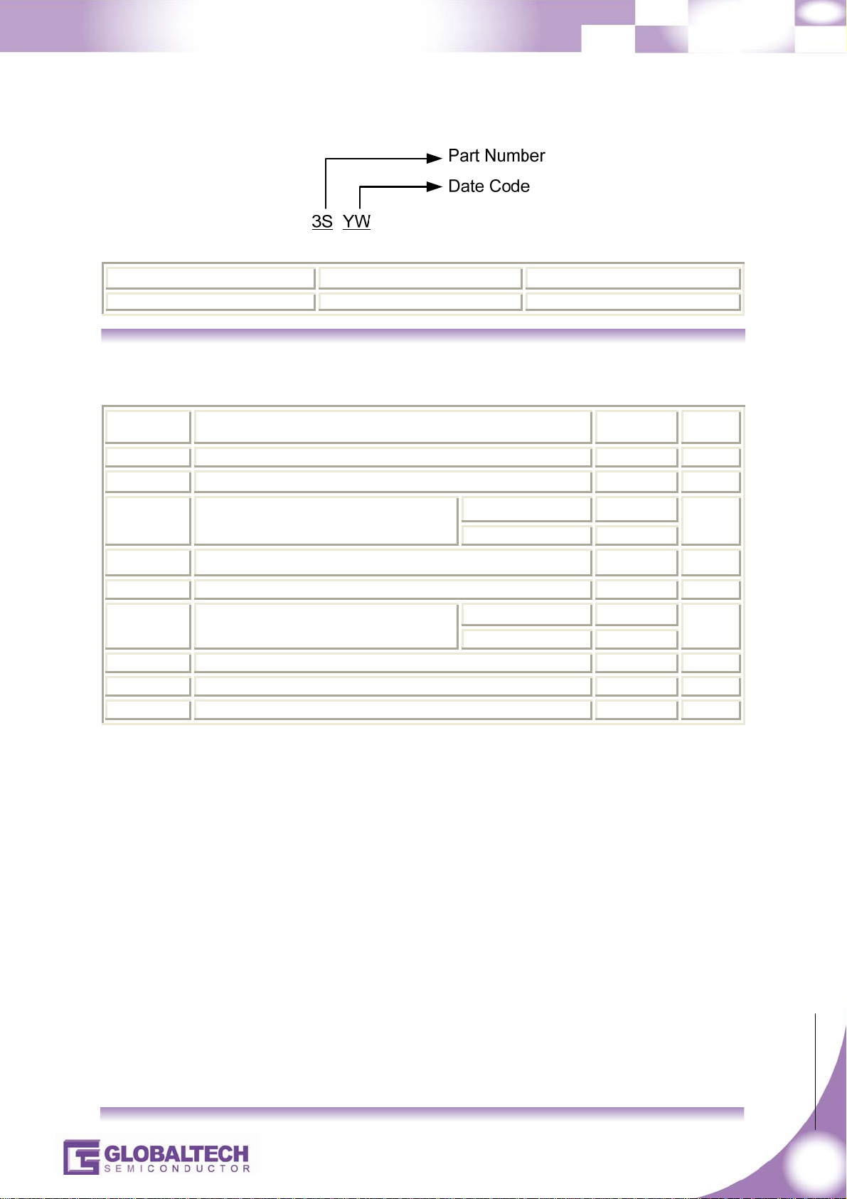
Marking Information
Part Number Package Part Marking
GSM9107ZF SOT-23-3L 3SYW
Absolute Maximum Ratings
TA=25ºC unless otherwise noted
Symbol Parameter Typical Unit
V
Drain-Source Voltage -30 V
DSS
V
Gate –Source Voltage ±12 V
GSS
I
Continuous Drain Current(T
D
=150ºC)
J
TA=25ºC
TA=70ºC
-4.0
-3.2
IDM Pulsed Drain Current -15 A
IS Continuous Source Current(Diode Conduction) -1.5 A
PD Power Dissipation
TA=25ºC
TA=70ºC
1.25
0.8
TJ Operating Junction Temperature 150 ºC
T
Storage Temperature Range -55/150 ºC
STG
R
Thermal Resistance-Junction to Ambient 120 ºC/W
JA
A
W
GSM9107
www.gs-power.com
2
Electrical Characteristics
TA=25ºC unless otherwise noted
Symbol Parameter Conditions Min Typ Max Unit
Static
V
(BR)DSS
V
GS(th)
I
Gate Leakage Current VDS=0V,VGS=±12V ±100 nA
GSS
I
DSS
I
On-State Drain Current
D(on)
Drain-Source
Breakdown Voltage
=0V,ID=-250uA -30
V
GS
Gate Threshold Voltage VDS=VGS,ID=-250uA -0.6 -1.1
Zero Gate Voltage
Drain Current
VDS=-24V,VGS=0V -1
VDS=-24V,VGS=0V
T
=85ºC
A
-30
VDS≦-5V,VGS=-4.5V -6 A
≦-5V,VGS=-2.5V -3
V
DS
V
uA
VGS=- 10V,ID=-4.0A 55 65
Drain-Source
On-Resistance
VGS=-4.5V,ID=-3.2A 65 80
R
DS(on)
VGS=-2.5V,ID=-1.0A 82 105
gfs
Forward
Transconductance
VDS=-5.0V,ID=-2.8A 6.5 S
VSD Diode Forward Voltage IS=-1.0A,VGS=0V -0.7 -1.3 V
Dynamic
Qg Total Gate Charge 10 18
=-15V,
V
Qgs Gate-Source Charge 1.6
Qgd Gate-Drain Charge
C
Input Capacitance 450
iss
C
Output Capacitance 95
oss
C
rss
t
8 18
d(on)
Reverse Transfer
Capacitance
Turn-On Time
tr
t
25 50
d(off)
Turn-Off Time
tf
DS
V
=-10V,ID-4.0A
GS
=-15V,
V
DS
V
=0V,f=1MHz
GS
V
=-15V,
DD
=15 ,ID-1.0A,
R
L
V
=-10V,RG=6
GEN
3.0
55
8 18
25 35
m
nC
pF
ns
GSM9107
www.gs-power.com
3
 Loading...