

150mA Low-Noise Ultra Low-Dropout Regulator
Product Description Features
The GS2615 is a 150 mA, fixed-output and
adjustable voltage regulator designed to provide
ultra low-dropout and low noise in battery powered
applications.
Using an optimized VIP
PNP) process, the GS2615 delivers unequalled
performance in all specifications critical to
battery-powered designs:
Dropout Voltage: Typically 300 mV @ 150 mA
load, and7 mV @ 1 mA load.
Ground Pin Current: Typically 850 μA @ 150 mA
load, and75 μA @ 1 mA load.
Enhanced Stability: The GS2615 is stable with
output capacitor ESR as low as 5 mΩ, which
allows the use of ceramic capacitors on the output.
Sleep Mode: Less than 1 μA quiescent current
when ON/ OFF pin is pulled low.
Smallest Possible Size: SOT-23-5L and micro
SMD packages use absolute minimum board
space.
Precision Output: 1% tolerance output voltages
available.
Low Noise: By adding a 10 nF bypass capacitor,
output noise can be reduced to 30 μV (typical).
Multiple voltage options, from 2.5V to 5.0V, are
available as standard products. Consult factory for
custom voltages.
TM
(Vertically Integrated
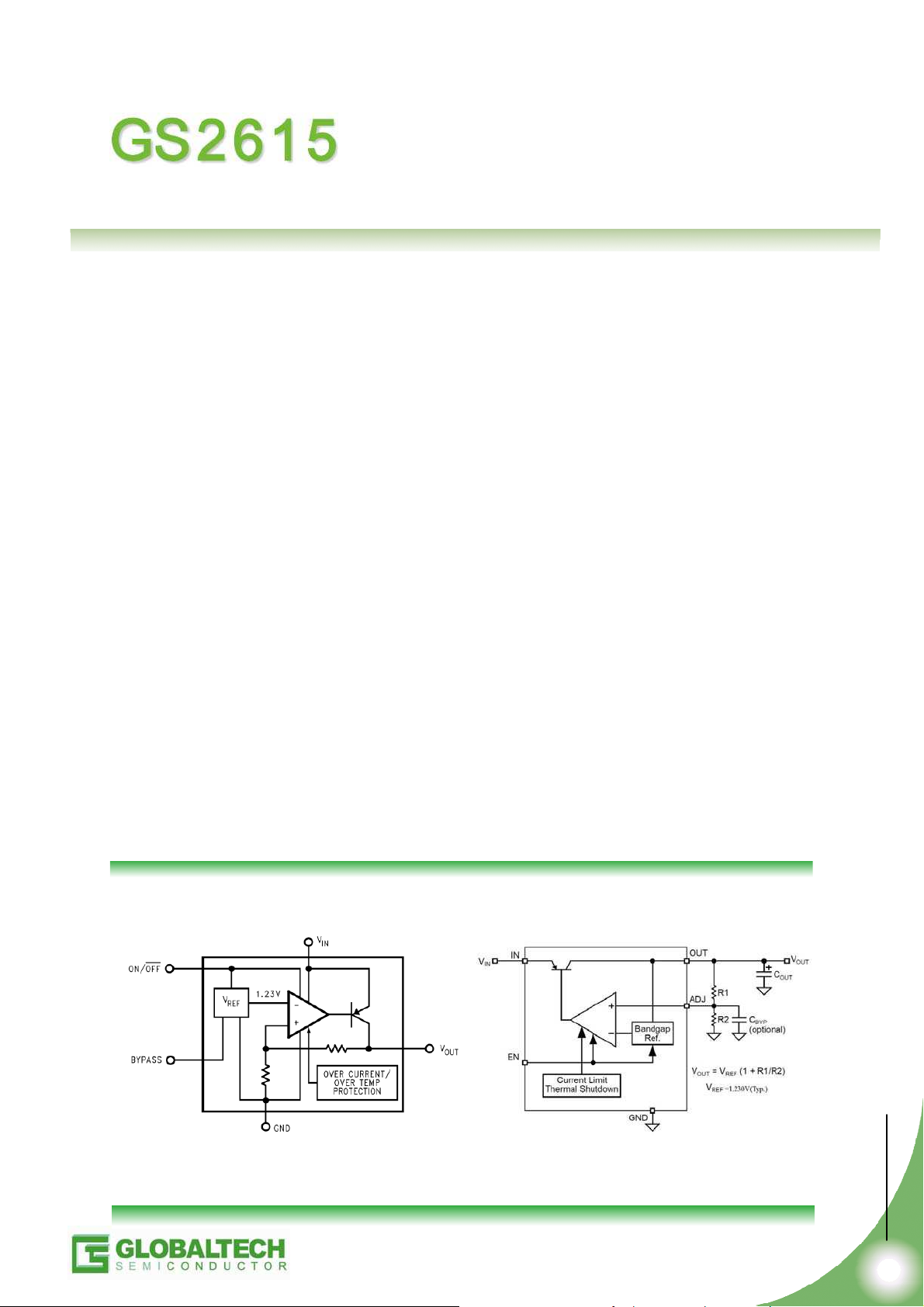
Block Diagram
Ultra low dropout voltage
Guaranteed 150 mA output current
Smallest possible size (SOT-23-5L, micro
SMD package)
Requires minimum external components
Stable with low-ESR output capacitor
<1 μA quiescent current when shut down
Low ground pin current at all loads
Output voltage accuracy 1%
High peak current capability
Wide supply voltage range (20V max)
Low Z
Over temperature/over current protection
−40°C to +125°C junction temperature range
Custom voltages available
: 0.3Ω typical (10 Hz to 1 MHz)
OUT
Applications
Cellular Phone
Palmtop/Laptop Computer
Personal Digital Assistant (PDA)
Camcorder, Personal Stereo, Camera
GS2615
www.gs-power.com
1
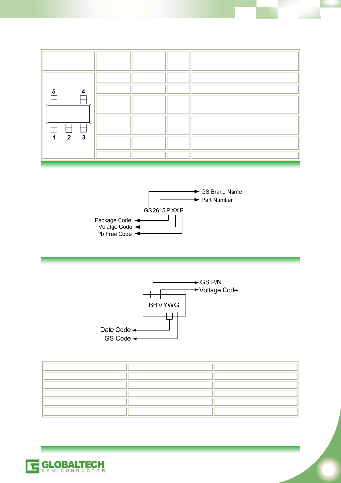
Packages & Pin Assignments
GS2615
(SOT-25)
GS2615-XX
(FIX)
Pin #
1 1 IN Supply Input
2 2 GND Ground
3 3 EN
4 - BYP
- 4 ADJ
5 5 OUT Regulator Output
Ordering Information
GS2615
(ADJ)
Pin #
Pin
Name
Pin Function
Enable/Shutdown:
CMOS compatible input. Logic high = enable,
logic low or open = shutdown.
Reference Bypass:
Connect external 470pF capacitor to GND to
reduce output noise. May be left open.
Adjustable regulator feedback input. Connect
to resistor voltage divider.
*For other voltages, please contact factory.
Marking Information
Part Number Marking Output
GS2615L BBA
GS2615L25
GS2615L30
GS2615L33
GS2615L50
BBH
BBQ
BBR
BBV
ADJ
WYG
WYG
WYG
WYG
WYG
2.5V
3.0V
3.3V
5.0V
GS2615
www.gs-power.com
2
Absolute Maximum Ratings (T
Symbol
=25°C Note1)
A
Parameter
Ratings Units
VIN Input Supply Voltage (survival) -0.6~+20 V
V
Input Supply Voltage (operating) 2.5~+20 V
INOP
ESD
PD
VO
IO I
V
IN-OUT
ESD Rating (Note 2)
Power dissipation (Note 3)
Output voltage (survival) (Note 4)
(survival) Short circuit protected
OUT
Input-Output voltage (survival) (Note 5)
2 kV
Internally limited
-0.3~+9 V
-0.3~+20 V
TOP Operating Temperature -40~+125 °C
T
Storage Temperature -65~+150 °C
STG
T
Lead Temp. (soldering, 5 sec.) 260 °C
LEAD
Electrical Characteristics(Fixed)
(unless otherwise specified: T
otherwise specified: V
IN
Symbol Parameter Condition Min Typ Max Unit
ΔVO Output voltage tolerance
Output voltage line
regulation
= 25°C. and limits in boldface type apply over the full operating temperature range. Unless
J
= VO(NOM) + 1V, I
= 1 mA, C
L
= 1 μF, C
IN
= 4.7 μF, V
OUT
ON/OFF
= 2V. )
IL=1mA -1.5 1.5
1mA ≤ I
1mA ≤ I
≤ 50mA
L
≤ 150mA
L
VO(NOM)+1V ≤ V
IL=0
≤ 20V
IN
-2.5 2.5
-3.5 3.5
-3.0 3.0
-4.0 4.0
0.007 0.014
0.032
1 3
5
7 10
IL=1mA
15
%V
NOM
%V
VIN-VO
V
ON/OFF
I
ON/OFF
I
GND
Dropout voltage (Note 7)
ON/OFF input voltage
(Note 8)
ON/OFF input current
Ground pin current
IL=10mA
40 60
90
IL=50mA
120 150
225
IL=150mA
280 350
575
High=O/P ON 1.4 1.6
Low=O/P OFF 0.15 0.55
V
=0V -2 0.01
ON/OFF
V
=5V 5 15
ON/OFF
IL=0
65 95
125
IL=1mA
75 110
170
=10mA
I
L
120 220
400
mV
V
µA
µA
GS2615
www.gs-power.com
3
Electrical Characteristics (Fixed Continue)
(unless otherwise specified: T
otherwise specified: V
IN
Symbol Parameter Condition Min Typ Max Unit
I
Ground pin current
GND
en
Output noise
voltage(RMS)
= 25°C. and limits in boldface type apply over the full operating temperature range. Unless
J
= VO(NOM) + 1V, I
= 1 mA, C
L
= 1 μF, C
IN
= 4.7 μF, V
OUT
IL=50mA
= 2V. )
ON/OFF
350 600
1000
IL=150mA
850 1500
2500
V
V
< 0.3V 0.01 0.8
ON/OFF
< 0.15V 0.05 2
ON/OFF
BW=300Hz to 50kHz
C
C
BYPASS
OUT
=10μF
=10nF
30 µV
µA
Ripple rejection
Io(SC) Short circuit current
Io(PK) Peak output current V
f=1kHz, C
C
BYPASS
=0(steady state)
R
L
(Note 9)
≥ VO(NOM)-5% 350 mA
OUT
=10μF
OUT
=10nF
45 dB
400 mA
Electrical Characteristics (Adjustable)
Symbol Parameter Condition Min Typ Max Unit
VO Output voltage IL=1mA
∆ VO /∆T
Output Voltage
temperature Coefficient
Output voltage line
regulation
V
+1V ≤ VIN ≤ 20V 0.007
O(NOM)
IL=1mA
40 ppm/ºC
IL=0
-1 0 1
-2 2
0.014
0.032
1 3
5
7 10
15
%V
%/V
NOM
V
IN -VO
Dropout voltage (Note 7)
IL=10mA
IL=50mA
I
=150mA
L
V
ON/OFF
I
ON/OFF
I
GND
ON/OFF input voltage
(Note 8)
ON/OFF input current
Ground pin current IL=0
High=O/P ON 1.4 1.6
Low=O/P OFF 0.15 0.55
V
=0V -2 0.01
ON/OFF
V
=5V 5 15
ON/OFF
40 60
90
120 150
225
280 350
575
65 95
125
mV
V
µA
µA
GS2615
www.gs-power.com
4
Electrical Characteristics (Adjustable Continue)
Symbol Parameter Condition Min Typ Max Unit
75 110
170
120 220
400
350 600
1000
850 1500
2500
50 µV
I
Ground pin current
GND
en
Output noise
voltage(RMS)
IL=1mA
IL=10mA
IL=50mA
IL=150mA
V
V
< 0.3V 0.01 0.8
ON/OFF
< 0.15V 0.05 2
ON/OFF
BW=300Hz to 50kHz
=10μF
C
OUT
BYPASS
=10nF
C
Ripple rejection
Io(SC) Short circuit current
Io(PK) Peak output current V
Note 1:
“Absolute Maximum Ratings” indicate limits beyond which damage to the component may occur.
Electrical specifications do not apply when operating the device outside of its rated operating
conditions.
Note 2:
The ESD rating of pins 3 and 4 for the SOT-23-5L package, or pins 5 and 2 for the micro SMD
package, is 1 kV.
Note 3:
The maximum allowable power dissipation is a function of the maximum junction temperature,
T
(MAX), the junction-to-ambient thermal resistance, Θ
J
maximum allowable power dissipation at any ambient temperature is calculated using:
Where the value of Θ
for the SOT-23-5L package is 220°C/W in a typical PC board mounting and
J-A
the micro SMD package is 225°C/W. Exceeding the maximum allowable dissipation will cause
excessive die temperature, and the regulator will go into thermal shutdown.
Note 4:
If used in a dual-supply system where the regulator load is returned to a negative supply, the
GS2615 output must be diode-clamped to ground.
Note 5:
The output PNP structure contains a diode between the V
reverse-biased. Reversing the polarity from V
Note 6:
Limits are 100% production tested at 25°C. Limits over the operating temperature range are
guaranteed through correlation using Statistical Quality Control (SQC) methods. The limits are used
to calculate National’s Average Outgoing Quality Level (AOQL).
Note 7:
Dropout voltage is defined as the input to output differential at which the output voltage drops 100
mV below the value measured with a 1V differential.
Note 8:
The ON/OFF input must be properly driven to prevent possible mis-operation. For details , refer to
Application Hints.
Note 9:
The GS2615 has foldback current limiting which allows a high peak current when V
then reduces the maximum output current as V
Characteristics curves).
Note 10:
Exposing the micro SMD device to direct sunlight will cause mis-operation. See Application Hints for
additional information.
f=1kHz, C
C
BYPASS
=0(steady state)
R
L
(Note 9)
≥ Vo(NOM)-5% 350 mA
OUT
=10μF
OUT
=10nF
to V
IN
OUT
40 dB
400 mA
, and the ambient temperature, TA. The
J-A
to V
IN
will turn on this diode.
OUT
is forced to ground (see Typical Performance
terminals that is normally
OUT
OUT
> 0.5V, and
GS2615
www.gs-power.com
5
Application Summary
EXTERNAL CAPACITORS
Like any low-dropout regulator, the GS2615 requires external capacitors for regulator stability. These capac itors
must be correctly selected for good performance.
Input Capacitor
An input capacitor whose capacitance is ≥ 1 μF is required between the GS2615 input and ground (the amount of
capacitance may be increased without limit).This capacitor must be located a distance of not more than 1 cm from
the input pin and returned to a clean analog ground. Any good qua lity ceramic, tantal um, or film capacit or may be
used at the input.
Important:
impedance source of power (like a battery or very large c apacitor). If a Tantalum capaci tor is used at the input, it
must be guaranteed by the manufacturer to have a surge current rating sufficient for the application.
There are no requirements for ESR on the input capacitor, but tolerance and tem perature coefficient must be
considered when selecting the capacitor to ensure the capacitance will be ≥ 1 μF over the entire operating
temperature range.
Output Capacitor
The GS2615 is designed specifically to work with ceramic output capacitors, utilizing circuitry which allows the
regulator to be stable across the entire range of output current with an output capacitor whose ESR is as lo w as 5
mΩ. It may also be possible to use.
Tantalum or film capacitors at the output, but these are not as attractive for reasons of size and c ost (see next
section Capacitor Characteristics).The output capacitor must meet the requirement for minimum amount of
capacitance and also have an ESR (equivalent series resistance) value which is within the stable range. Curves
are provided which show the stable ESR range as a function of load current (see ESR graph below).
Tantalum capacitors can suffer catastrophic failure due to surge current when conn ected to a low
Important:The output capacitor must maintain its ESR within the stable region over the full operating temperature
range of the application to assure stability.
The GS2615 requires a minimum of 2.2 μF on the output (output capacitor size can be increased without limit).
It is important to remember that capacitor tolerance and variation with temperature must be taken into
consideration when selecting an output capacitor so that the minimum requir ed amount of output capacitance is
provided over the full operating temperature range. It should be noted that ceramic capacitors can exhibit large
changes in capacitance with temperature (see next section, Capacitor Characteristics).
The output capacitor must be located not more than 1 cm from the output pin and returned to a clean analog
ground.
Noise Bypass Capacitor
Connecting a 10 nF capacitor to the Bypass pin significantly reduces noise on the regulator output. It should be
noted that the capacitor is connected directly to a high-impedance circuit in the band gap reference.
Because this circuit has only a few microamperes flowing in it, any si gnificant loading on this node will cause a
change in the regulated output voltage. For this reason, DC leakage curr ent through the noise bypass capacitor
www.gs-power.com
GS2615
6

must never exceed100 nA, and should be kept as low as possible for best output voltage accuracy.
The types of capacitors best suited for the noise bypass capacitor are ceramic and film. High-quality ceramic
capacitors with either NPO or COG dielectric typically have very low leakage. 10 nF polypropolene and
polycarbonate film capacitors are available in small surface-mount packages and typically have extremely low
leakage current.
Adjustable Regulator Applications
The GS2615 can be adjusted to a specific output voltage by using two external resistors (see Application circuit).
The resistors set the output voltage based on the following equation:
This equation is correct due to the configuration of the bandga p reference. The bandgap voltage is relative to the
output, as seen in the block diagram. Traditional regulators normally have the reference voltage relativ e to ground
and have a different VOUT equation. Resistor values are not critical because ADJ (adjust) has a high input
impedance, but for best results use resistors of 470kΩ or less. A capacitor from ADJ to ground provides greatly
improved noise performance.
CAPACITOR CHARACTERISTICS
The GS2615 was designed to work with ceramic capacitors on the output to take advantage of the benefits they
offer: for capacitance values in the 2.2 μF to 4.7 μF range, ceramics
are the least expensive and also have the lowest ESR values (which makes them best for eliminating high
frequency noise). The ESR of a typical 2.2 μF ceramic capacitor is in the range of 10 mΩ to 20 mΩ, which easily
meets the ESR limits required for stability by the GS2615. One disadvantage of ceramic capacitors is that their
capacitance can vary with temperature. Most large value ceramic capacitors (≥ 2.2 μF) are manufacture d with the
Z5U or Y5V temperature characteristic, which results in the capacitance dropping by more than 50% as the
temperature goes from 25°C to 85°C.
This could cause problems if a 2.2 μF capacitor were used on the output since it will drop down to approximately 1
μF at high ambient temperatures (which could cause the GS2615 to oscillate). If Z5U or Y5V capacitors are used
on the output, a minimum capacitance value of 4.7 μF must be observed.
A better choice for temperature coefficient in ceramic capacitors is X7R, which holds the capacitance within ±15%.
Unfortunately, the larger values of capacitance are not offered by all manufacturers in the X7R dielectric.
Tantalum
Tantalum capacitors are less desirable than ceramics for use as output capacitors because they are more
expensive when comparing equivalent capacitance and voltage ratings in the1 μF to 4.7 μF range.
Another important consideration is that T ant alum capacitors have higher ESR values than equivalent size ceramics.
This means that while it may be possible to find a Tantalum capacitor with an ESR value within the stable range, it
would have to be larger in capacitance (which means bigger and more costly) than a ceramic capacitor with the
same It should also be noted that the ESR of a typical Tantalum will increase about 2:1 as the temperature goes
from 25°C down to −40°C, so some guard band must be allowed.
GS2615
www.gs-power.com
7

On/off Input Operation
The GS2615 is shut off by driving the ON/OFF input low, and turned on by pulling it high. If this feature is not to be
used, the ON/OFF input should be tied to VIN to keep the regulator output on at all times.
To assure proper operation, the signal source used to drive the ON/OFF input must be able to swing abov e and
below the specified turn-on/turn-off voltage thresholds listed in the Electrical Characteristics section under V
ON/OFF
To prevent mis-operation, the turn-on (and turn-off) voltage signals applied to the ON/OFF input must h ave a slew
rate which is≥ 40 mV/μs.
Caution: the regulator output voltage can not be guaranteed if a slo w-moving AC (or DC) signal is ap plied that is
in the range between the specified turn-on and turn-off voltages listed under the electrical specification V
Electrical Characteristics).
ON/OFF
(see
REVERSE INPUT-OUTPUT VOLTAGE
The PNP power transistor used as the pass element in the GS2615 has an inherent diode connected between the
regulator output and input. During normal operation (where the input voltage is higher than the output) this diode is
reverse biased.
However, if the output is pulled above the input, this diode will turn ON and current will flow into the regulator output.
In such cases, a parasitic SCR can latch which will allow a high current to flow into V
which can damage the part.
(and out the ground pin),
IN
In any application where the output may be pulled above the input, an external schottk y diode must be connected
from V
to V
IN
Absolute Maximum Ratings).
(cathode on VIN, anode on V
OUT
), to limit the reverse voltage across the GS2615 to 0.3V (see
OUT
MICRO SMD MOUNTING
The micro SMD package requires specific mounting techniques which are detailed in National Semiconductor
Application Note # 1112. Referring to the section Surface Mount Technology (SMT) Assembly Considerations,
it should be noted that the pad style which must be used with the 5-pin package is the NSMD (non-solder mask
defined) type.
For best results during assembly, alignment ordinals on the PC board may be used to facilitat e placement of the
micro SMD device.
MICRO SMD LIGHT SENSITIVITY
Exposing the micro SMD device to direct sunlight will cause mis-operation of the device. Light sources such as
Halogen lamps can also affect electrical performance if brought near to the device.
The wave lengths which have the most detrimental effect are reds and infr a-reds, which mean that the fluorescent
lighting used inside most buildings has very little effect on performanc e. A micro SMD test board was brought to
within 1 cm of a fluorescent desk lamp and the effect on the regulated output voltage was negligible, showing a
deviation of less than 0.1% from nominal.
.
Application Current
GS2615
www.gs-power.com
8

Typical Performance Characteristics
Unless otherwise specified: C
V
vs Temperature Short-Circuit Current
OUT
Short-Circuit Current Short Circuit Current vs Output Voltage
= 1μF, C
IN
= 4.7μF, V
OUT
= V
(NOM) +1, T
OUT
IN
= 25°C, ON/OFF pin is tied to VIN.
A
Ripple Rejection Ripple Rejection
GS2615
www.gs-power.com
9

Typical Performance Characteristics(Continue)
Ripple Rejection Ripple Rejection
Ripple Rejection Ripple Rejection
Ripple Rejection Ripple Rejection
GS2615
www.gs-power.com
10

Typical Performance Characteristics(Continue)
Ripple Rejection Output Impedance vs Frequency
Output Impedance vs Frequency Output Noise Density
Output Noise Density Ground Pin vs Load Current
GS2615
www.gs-power.com
11

Typical Performance Characteristics(Continue)
Dropout Voltage vs Temperature Input Current vs Pin
GND Pin Current vs Temperature Instantaneo us Short Circuit Current
Load Transient Response Load Transient Response
GS2615
www.gs-power.com
12

Typical Performance Characteristics(Continue)
Load Transient Response Line Transient Response
Line Transient Response Line Transient Response
Line Transient Response Turn-On Time
GS2615
www.gs-power.com
13
Typical Performance Characteristics(Continue)
Turn-On Time Turn-On Time
Turn-On Time
GS2615
www.gs-power.com
14

Package Dimension
SOT-23-5L PLASTIC PACKAGE
D
e1
A
SYMBOL
A1
A1
A2
E1
e1
L1
A
b
c
D
E
e
L
G
θ
A2
E
E1
L
θ
e
b
c
(L1)
G
Dimensions
Millimeters Inches
MIN MAX MIN MAX
0.95 1.45 .037 .057
0.05 0.15 .002 .006
0.90 1.30 .035 .051
0.30 0.50 .012 .020
0.08 0.20 .003 .008
2.80 3.00 .110 .118
2.60 3.00 .102 .118
1.50 1.70 .059 .067
0.95 (TYP) .037 (TYP)
1.90 (TYP) .075 (TYP)
0.35 0.55 .014 .022
0.60 (TYP) .024 (TYP)
0.25 (TYP) .010 (TYP)
0° 8° 0° 8°
GS2615
www.gs-power.com
15

NOTICE
Information furnished is believed to be accurate and reliable. However Globa ltech Semiconductor assumes no
responsibility for the consequences of use of such information nor for any infringement of patents or other rights of
third parties, which may result from its use. No license is granted by implication or otherwise under any patent or
patent rights of Globaltech Semiconductor. Specifications mentioned in this publication are subject to change
without notice. This publication supersedes and replaces all information without express written approval of
Globaltech Semiconductor.
CONTACT US
4F.,No.43-1,Lane11,Sec.6,Minquan E. Rd Neihu District T aipei City 114, Taiwan (R.O.C)
886-2-2657-9980
886-2-2657-3630
sales_twn@gs-power.com
GS Headquarter
Wu-Xi Branch
No.21 Changjiang Rd., WND, Wuxi, Jiangsu, China (INFO. &. TECH. Science Park Building A 210 Room)
86-510-85217051
86-510-85211238
sales_cn@gs-power.com
RD Division
824 Bolton Drive Milpitas. CA. 95035
1-408-457-0587
Version_1.4
Notice

 Loading...