

Page 1

GRUNDIG
W70-1021
Product code: 564383
SERVICE MANUAL
June, 10th 2002
CONTENTS: (E12)
1. PRODUCT SPECIFICATIONS & FEATURES : PAGE 2
2. BLOCK DIAGRAM : PAGE 3,4,5,6
3. COMPONENT LOCATION : PAGE 7,8
4. SET-UP PROCEDURE &
ALIGNMENT INSTRUCTIONS : PAGE 9-17
5. IC PIN DETAILS : PAGE 18-22
6. PCB LAYOUTS : PAGE 23
7. EXPLODED VIEW, MANUF. PARTS : PAGE 24,28
8. PART LIST : PAGE 25-27
9. CIRCUIT DIAGRAMS : PAGE 29-31
1
Page 2
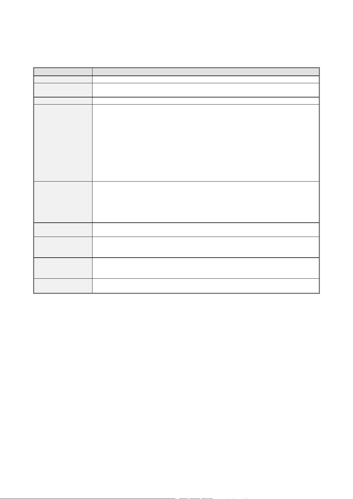
PRODUCT SPECIFICATION & FEATURES
TVTEXT Version 7p (SDA 5553-A009/EV E945)
1. SCREEN SIZE:
2. AVAILABLE
STANDARDS:
3. TUNER:
4. FEATURES:
5. SOUND:
6. TELETEXT:
7. CONNECTIONS:
8. VIDEO:
9. CONSUMPTION:
28”
PAL I,
HYPERBAND: VHF 2-12, UHF 21-69, S1-S41
Frequency synt. (62,5KHz search steps),
MENU oriented OSD (On Screen Disp.) Multilanguage MENU OSD,
100 programs,
Full function remote control,
Automatic switch off at the end of the progr.
Off timer 0 - 120 min.,
Organise Program Informatio n System (OPIS) with the following functions:
• Autostore with simple ATS: Autostore, Name, Order,
• Insert
• Delete
• Rename,
MONO/STEREO/DUAL sound decoder,
Virtual Dolby sound,
NICAM Digital Stereo Sound Processor,
Muting,
2 loudspeakers,
Audio music power: 2x15W (STEREO),
7 - page TTX with FLOF and P26,
Westeuropean and easteuropean language support.
SCART I AV connector (21 - pin) video, RGB and SVHS,
SCART II AV connector (21 - pin) video
Antenna connection 75 ohms unbalanced,
Blue stretch,
Automatic Colour limiting,
Colour Temperature adjustment,
≈95W; <9W stand by;
POWER REQUIREMENTS: Voltage/frequency: 230V/50Hz , rating (180V - 250V)
2
Page 3

BLOCK DIAGRAM: MODULES ARRANGEMENT ON CHASSIS
L
R
E12 CHASSIS
MODULES & CONNECTION
21.5.2002
3
Page 4

BLOCK DIAGRAM – MODULES & CONNECTIONS
2
AUDIO
SREREO
AUDIO
VK-E9T
TDA6107
IC201
R
L
K101B
2
K104
OUT
TDA7057A
IC102
PROC.
MSP34XXG
IC503
K102A
RGB
V+V-GUARD
7
RGB
K704
4
2
K301
VERT.
OUT
TDA8356-90°
TDA8351-110°
CRT SOCKET
K703B K704B
K752
H. DRIVE
K703A K704A
EW DRIVE
H. FLY
LZ-E9
IC301
Z_COR
2
E12 CHASSIS
BLOCK DIAGRAM
MODULES & CONNECTIONS
6.6.2002
K701
K702A
HOR.
OUT
BU508A
T701
42V
15V
EHT COMP
BEAMCURR
R,G,B,BL
SC1
200V
L,R
K105
SCART 1
IF
U4468B
IC501
R,G,B,BL
R,G,B,BL IN
R G B
SWITCH
74HCT4053
IC801
CVBS_SC1
CVBS_INT
SIGNAL &
SAW
TUNER
E12
DEFL. PROC.
filter
F108
TUN101
CVB
S_EXT
VIDEO
SWITCH
TEA2014
TDA884X
IC101
K6
SDA5553
CONTROL
& TEXT
IC1
PROC.
K901A
IC104
A
T
8,5V
33V
12V
15V
155V
POWER
SUPPLY
K106
SCART 2
CVB
S
_
SC2
A1
A2
2,5V
2,5V
5V
8V
TDA4605-2
2,5V
3,3V
BUZ90A
IC601
T602
K601
5
230V AC
4
Page 5
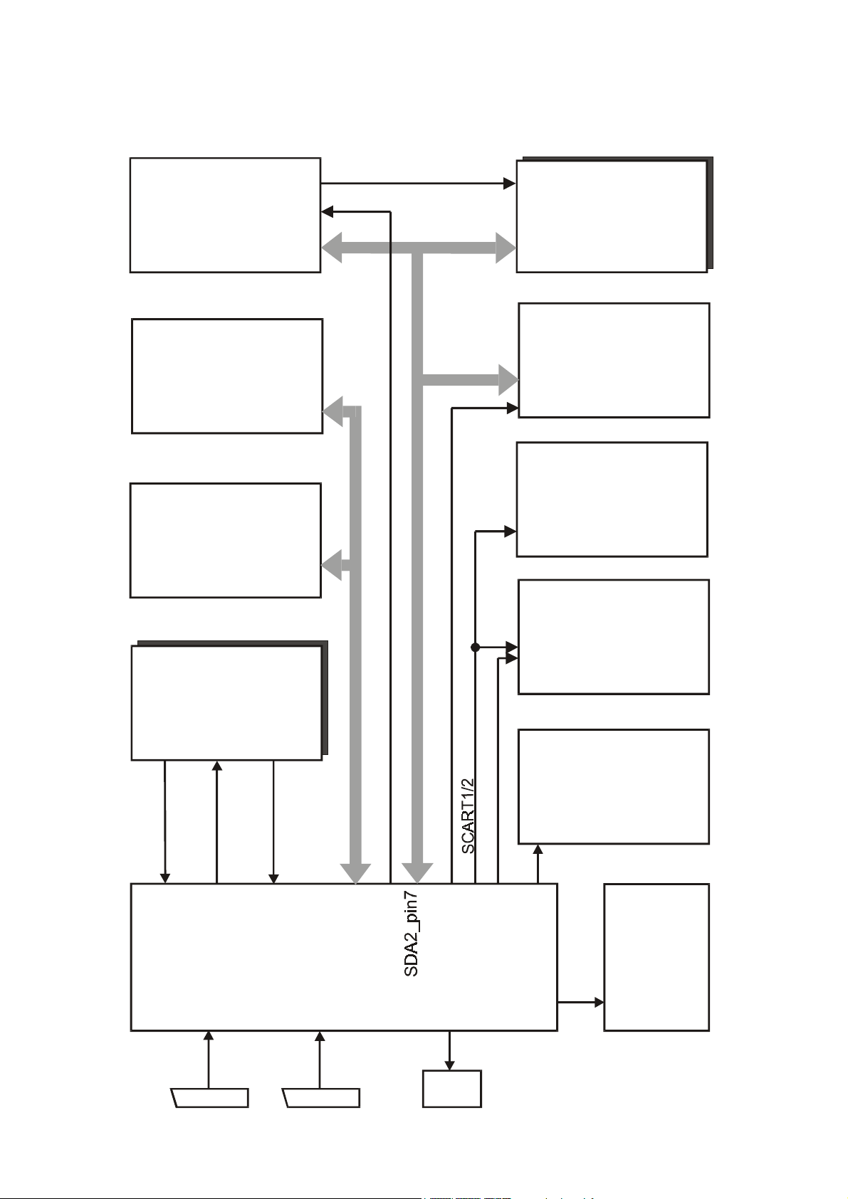
BLOCK DIAGRAM – CONTROL SIGNALS
SIGNAL &
DEFL. PR.
IC101
EEPROM
IC1
EEPROM
IC2
pin54
pin26
SCL_pin7
SDA_pin8
SDA_pin5
SCL_pin6
SDA_pin5
SCL_pin6
AGC
IIC1
2
C
I
I
pin5
TUNER
TUN101
SCL_pin4
SDA_pin5
STEREO PROC.
IC503
SCL_pin7
SDA_pin8
pin20
VIDEO SW.
IC104
pin5
RGB SW.
SFTLA_E9
TPA_CG
A
1
0
9
K
B
Y
E
K
pin
15
A
1
)
1
(
0
9
K
D
E
L
pin
46
)
2
(
CONTR. &
TEXT PROC .
IC1
pin
16
1
I
R
E
P
SC1
8
K901A
5
C
R
pin
24
(3)
pin
17
SC2
2
I
R
E
P
5
n
i
p
_
1
A
D
S
8
1
C
S
_
L
B
4
6
n
n
i
i
p
p
_
1
L
C
S
DECODER
T107
8
n
i
p
_
2
L
C
S
pin
3
IC801
pin9,10,11
ON/OFF SW.
T9, T601, T603
V
T
/
V
RESET
A
ON/OFF
3
7
2
2
n
n
i
i
p
p
1
1
2
n
n
i
i
p
p
AUDIO
OUT
IC102
pin
VOL pin
51
1,7
5
Page 6
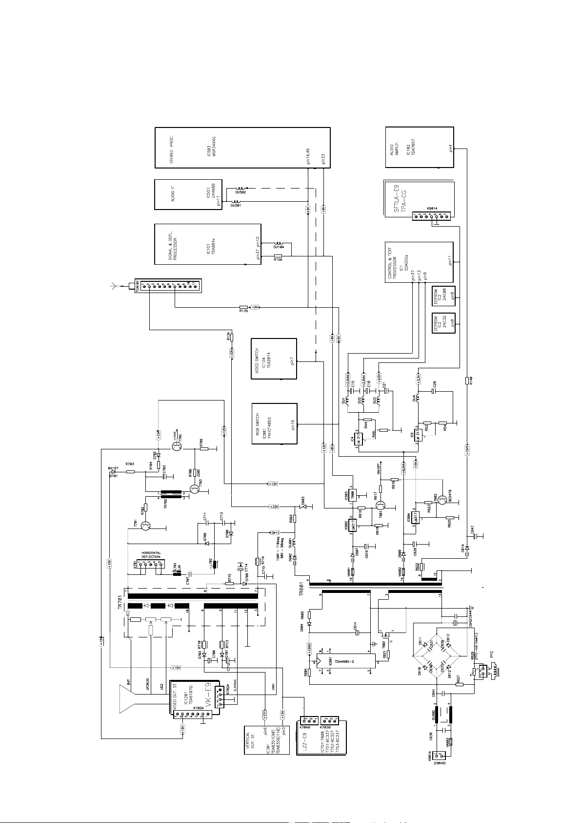
BLOCK DIAGRAM - SUPPLY VOLTAGES
6
Page 7

COMPONENT LOCATION AND MEASURING POINTS FOR
V
SUPPLY VOLTAGES ON MAIN CHASSIS – COMPONENT SIDE
155V adjust 200V155V
A
8,5V
A1
2,5V
2,5V2,5V
A2
3,3V
15V
T
15V
42V
12V
8V
5
33V
7
Page 8

COMPONENT LOCATIONS ON SEPARATE MODULES OF CHASSIS E12 –
COMPONENT SIDE
VK-E9TM
TPA-CG
8
Page 9
SETUP PROCEDURE & ALIGNMENT INSTRUCTIONS
All necessary adjustments and settings are performed during manufacture of TV set and assure its
correct operation when connected to the mains voltage and antenna or external video or audio signal.
When TV set requires service intervention all settings should be checked and corrected, if necessary.
DEMAGNETISING OF PICTURE TUBE
Correctness o f picture tube d emagnetising i s usually automati cally checked . Magnetisatio n of picture
tube is presented as one or more colour "clouds", consequently colour reproduction of the picture is
not correct.
Each time the TV set is switched on with mains switch, demagnetising system is activated. For correct
demagnetising procedure disconnect the TV set with mains switch and leave it disconnected for about
15 minutes. Afterwards when you switch on the TV, demagnetising procedure is performed. In case
distortion of colour reproduction still persists, special demagnetising coil should be used.
ADJUSTMENT ADJUSTMENT
CONDITION
1. SUPPLY VOLTAGE
FOR HORIZONTAL
OUTPT STAGE
»B+«
SWITCHING TO SERV ICE MODE
All other service settings of TV set are made in so called service mode of TV set operation. To enter this mode of operation press
the keys in the following sequence: "TV", "I", and "STOP" in the period of 5 seconds from switching on the TV set to normal mode
of operation. When the TV set is switched over to service mode the following status line with service parameter and parameter value
appears on the screen:
SERVICE PARAM: XX VALUE: xx
The parameter to be set is selected with keys (P+/P-), and selected parameter is set with keys (volume+ /volume-). Each
time you press the key for parameter selection ( ) the value of preselected parameter is stored. Therefore when the last setting is
performed you must press one of the two keys once again. Values of individual parameters are expressed in hexadecimal form due
to limited capacity of the memory. Values of individual parameters are variable from 0 to 3F, with the exception of some parameters
(see the table at the end of describing service mod e) where values are changed fro m 0 to 7F and O1, O2, O3, O4, O5 which have
value range between 0 an d FF.
When setting is finished it should obligatory be concluded with "STOP" key. After a few seconds the status line disappears and
service adjustment is accomplished.
• Connect the TV set to
supply voltage
175…250VAC.
• Switch it on and set it by
means of remote
controller to AV mode of
operation.
• Connect DC voltmeter to
D-602 cathode.
With P-601 potentiometer set supply voltage for
horizontal output stage to:
ADJUSTMENT ACTIVITY
AND RESULT OF SETTINGS
• 152V ±±±±0,5V
NOTE: In case service adjustment is not ended in above specified mode (e.g. power supply breakdown), the
adjustment should be repeated.
2. VERTICAL
PICTURE
POSITION
• To antenna connector of
TV set, which is switched
on and operates in service
mode, connect VF signal
source with PHILIPS test
picture.
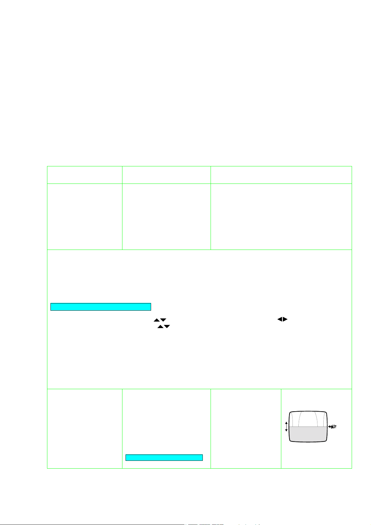
• Select the following service
setting on the screen:
SERVICE PARAM: VH VALUE: xx
• With remote
controller set vertical
position of the
picture: beginning of
dark part of the
picture should be
exactly in the centre
of the screen (two
bright points on left
and right side of the
screen).
9
Page 10

ADJUSTMENT ADJUSTMENT
CONDITION
3. VERTICAL
AMPLITUDE
ON TOP PART
OF SCREEN
4. VERTICAL
AMPLITUDE ON
BOTTOM PART
OF SCREEN
• To antenna connector of TV
set, which is switched on
and operates in service
mode, connect VF signal
source with PHILIPS test
picture.
• Select the following service
setting on the screen:
SERVICE PARAM: VA VALUE: xx
• To antenna connector of
TV set, which is switched
on and operates in service
mode, connect VF signal
source with PHILIPS test
picture.
• Select the following service
setting on the screen:
SERVICE PARAM: VS VALUE: xx
ADJUSTMENT ACTIVITY
AND RESULT OF SETTINGS
• With remote
controller set vertical
amplitude of picture
on top, visible part of
the screen. The
beginning of test
picture should be at
the beginning of top
part of the screen.
• With remote
controller set vertical
amplitude of picture
on bottom part of the
screen. The lower
part of test picture
should be at the edge
of bottom part of the
screen. During this
setting the picture on
top part of the screen
should not change.
5. CORRECTION OF
"S" VERTICAL
PICTURE
DISTORTION
6. HORIZONTAL
PICTURE
POSITION
• To antenna connector of TV
set, which is switched on
and operates in service
mode, connect VF signal
source with PHILIPS test
picture.
• Select the following service
setting on the screen:
SERVICE PARAM: SC VALUE: xx
• To antenna connector of
TV set, which is switched
on and operates in service
mode, connect VF signal
source with PHILIPS test
picture.
• Select the following setting
on the screen:
SERVICE PARAM: HS VALUE: xx
• With remote
controller correct the
picture. The distances
between the two
horizontal lines of
test picture in the
centre of the screen
should be equal to the
distances on top and
bottom part of the
screen. If after this
setting vertical
amplitude of picture
changes, see pos. 5
and 6.
• With remote
controller set test
picture to the centre
of the screen (if
necessary first widen
the picture, see pos.
7).
10
Page 11
ADJUSTMENT ADJUSTMENT
CONDITION
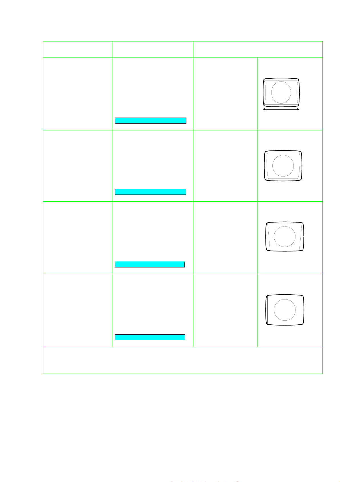
7. HORIZONTAL
AMPLITUDE
OF PICTURE
• To antenna connector of TV
set, which is switched on
and operates in service
mode, connect VF signal
source with PHILIPS test
picture.
• Select the following service
setting on the screen:
SERVICE PARAM: EW VALUE: xx
ADJUSTMENT ACTIVITY
AND RESULT OF SETTINGS
• With remote
controller set picture
width. Edges of test
picture should be just
hidden behind the
edges of the screen.
8. CORRECTION OF
PICTURE
HORIZONTAL
PINCUSHION
DISTORTION
9. CORRECTION OF
PICTURE
HORIZONTAL
PINCUSHION
DISTORTION IN
CORNERS OF THE
SCREEN
10. CORRECTION OF
PICTURE
TRAPEZIUM
DISTORTION
• To antenna connector of
TV set, which is switched
on and operates in service
mode, connect VF signal
source with PHILIPS test
picture.
• Select the following service
setting on the screen:
SERVICE PARAM: PW VALUE: xx
• To antenna connector of TV
set, which is switched on
and operates in service
mode, connect VF signal
source with PHILIPS test
picture.
• Select the following service
setting on the screen:
SERVICE PARAM: CP VALUE: xx
• To antenna connector of
TV set, which is switched
on and operates in service
mode, connect VF signal
source with PHILIPS test
picture.
• Select the following service
setting on the screen:
• With remote
controller correct the
picture. On left and
right side of test
picture straight lines
should appear
(especially in the
centre of the
picture).
• With remote
controller correct the
picture. On left and
right part of test
picture straight lines
should appear also in
corners of the screen.
• With remote
controller correct the
picture. On left and
right part of test
picture perfectly
straight and vertical
lines should appear.
SERVICE PARAM: TC VALUE: xx
REMARK:
If after correcting pincushion and trapezoidal distortion, changes the horizontal amplitude of picture, is necessary to
correct also horizontal amplitude of picture according to explanation in point 7.
11
Page 12
ADJUSTMENT ADJUSTMENT
CONDITION
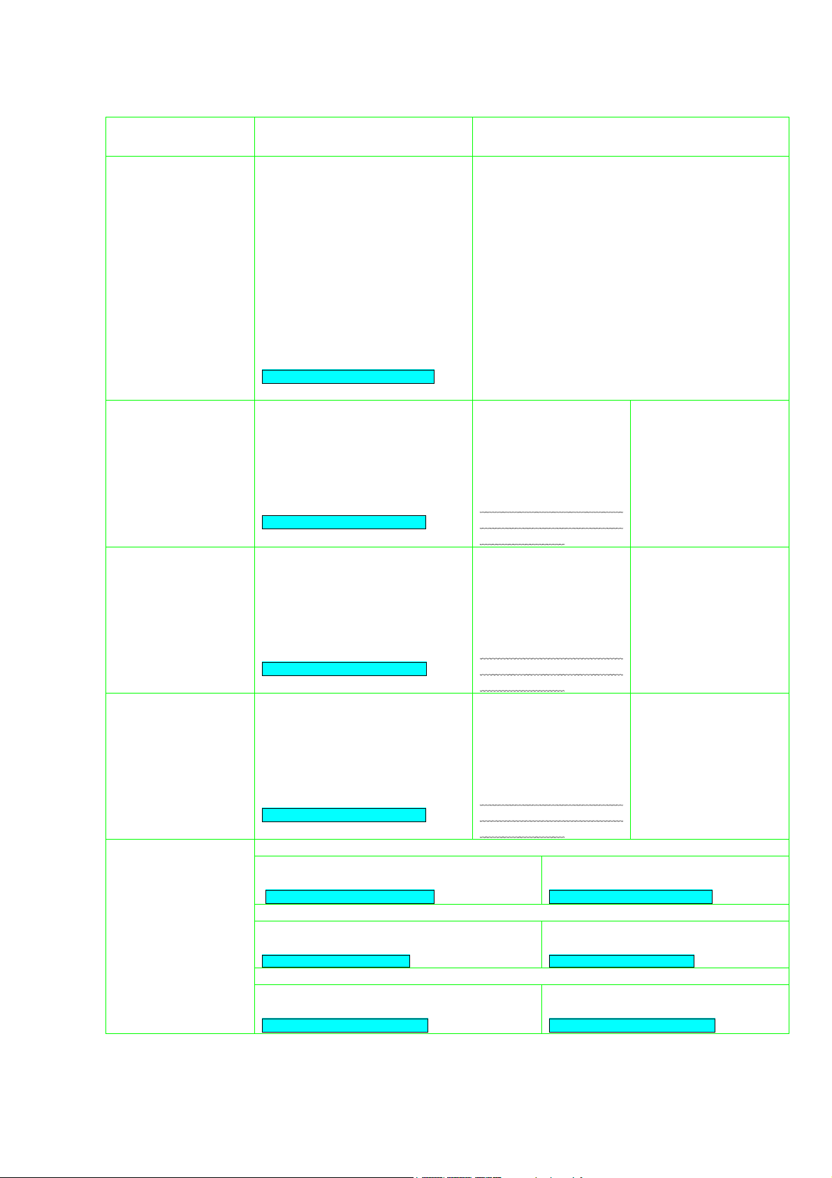
11. OPERATING
THRESHOLD OF
AUTOMATIC
AMPLIFICATION
REGULATION
• To antenna connector of TV
set, which is set to channel 12,
connect VF signal source of
frequency 224,25 MHz (C12)
with RF amplitude 60dB/uV
(1mV/75E).
• Connect voltmeter, dc, on
C107.
• Switch the TV set to service
mode of operation.
• Select the following service
setting:
SERVICE PARAM: AC VALUE: xx
ADJUSTMENT ACTIVITY
AND RESULT OF SETTINGS
• With remote controller keep changing the value
of AC setting until 7.5V±0,5V appears on
voltmeter display.
REMARK: If in chassis is inserted WW form of
tuner (small casing), with 5V supply, set on
voltmeter value 2,8V±0,1V.
12. RED
COMPONENT
OF WHITE
13. GREEN
COMPONENT
OF WHITE
14. BLUE
COMPONENT
OF WHITE
15. REFERENCE
OSCILLATING
CIRCUIT OF
DEMODULATOR
• To antenna connector of TV
set, which is switched on and
operates in service mode,
connect VF signal source with
PHILIPS test picture.
• With remote
controller set value:
1F: Pict. Tube Philips,
Panasonic.
1F: Pict. Tube Thomson.
• Select the following service
setting:
SERVICE PARAM: R VALUE: xx
This value is for
orientation and depends
of picture tube.
• To antenna connector of TV
set, which is switched on and
operates in service mode,
connect VF signal source with
PHILIPS test picture.
• With remote
controller set value:
24: Pict. Tube Philips,
Panasonic.
28: Pict. Tube Thomson.
• Select the following service
setting:
SERVICE PARAM: G VALUE: xx
This value is for
orientation and depends
of picture tube.
• To antenna connector of TV
set, which is switched on and
operates in service mode,
connect VF signal source with
PHILIPS test picture.
• With remote
controller set value:
24: Pict. Tube Philips,
Panasonic.
20: Pict. Tube Thomson.
• Select the following service
setting:
SERVICE PARAM: B VALUE: xx
This value is for
orientation and depends
of picture tube.
PAL /SECAM BG/L
• With remote controller select the following
service setting:
SERVICE PARAM: I1 VALUE: xx
PAL /SECAM /L'
• With remote controller select the following
service setting:
SERVICE PARAM: I2 VALUE: 00
PAL /SECAM /DK
• With remote controller select the following
service setting:
SERVICE PARAM: I3 VALUE: 40
• With keys for set val ue cha ngin g set
parameter value.
SERVICE PARAM: I1 VALUE:40
• With keys for set val ue cha ngin g set
parameter value.
SERVICE PARAM: I2 VALUE: 00
• With keys for set val ue cha ngin g set
parameter value.
SERVICE PARAM: I3 VALUE: 40
12
Page 13
ADJUSTMENT ADJUSTMENT CONDITION ADJUSTMENT ACTIVITY
AND RESULT OF SETTINGS
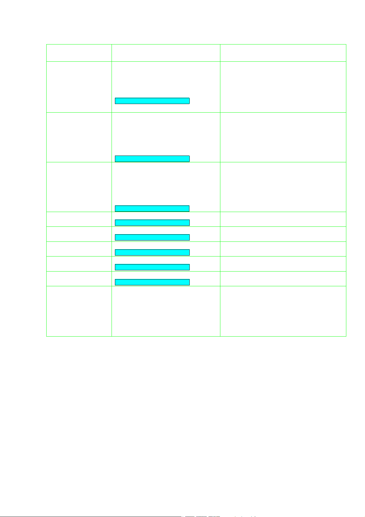
16. TIME DELAY
OF
LUMINANCE
SIGNAL
17. HORIZONTAL
OSD POSITION
18. OSD COLOUR
INTENSITY
19. OPTION BYTE 1
20. OPTION BYTE 2
21. OPTION BYTE 3
22. OPTION BYTE 4
23. OPTION BYTE 5
24. VOLTAGE FOR
PICTURE TUBE
BEAM
FOCUSING
• To antenna connector of TV set,
which is switched on and operates in
service mode, connect VF signal
source with PHILIPS test picture.
• Select the following setting:
SERVICE PARAM: YD VALUE:xx
• To antenna connector of TV set,
which is switched on and operates in
service mode, connect VF signal
source with PHILIPS test (or any)
picture.
• Select the following setting:
SERVICE PARAM: HD VALUE:xx
• To antenna connector of TV set,
which is switched on and operates in
service mode, connect VF signal
source with PHILIPS test (or any)
picture.
• Select the following setting:
SERVICE PARAM: RG VALUE:xx
• Select the following setting:
SERVICE PARAM: O1 VALUE: xx
• Select the following setting:
SERVICE PARAM: O2 VALUE: xx
• Select the following setting:
SERVICE PARAM: O3 VALUE: xx
• Select the following setting:
SERVICE PARAM: O4 VALUE: xx
• Select the following setting:
SERVICE PARAM: O5 VALUE: xx
• Switch the colour TV with STOP
key on remote controller to normal
mode of operation.
• Connect signal with Philips test
picture to antenna connector.
• With remote controller set such delay
setting that signals of colour and black white picture overlap.
Recommended value: D
• With remote controller set position of the
OSD (On Screen Display) to the centre of
the screen.
• With remote controller set colour intensity
(4 steps) of the OSD (On Screen Display).
• See table of OPTION BYTES on followed
pages.
• See table of OPTION BYTES on followed
pages.
• See table of OPTION BYTES on followed
pages.
• See table of OPTION BYTES on followed
pages.
• See table of OPTION BYTES on followed
pages.
• With potentiometer for focusing voltage
adjustment on HV transformer set such
value of volta ge, tha t give s shar p pict ure on
entire surface of the screen. Sharpness
should be equal in corners and in centre of
the screen.
13
Page 14
ADJUSTMENT ADJUSTMENT CONDITION ADJUSTMENT ACTIVITY
AND RESULT OF SETTINGS
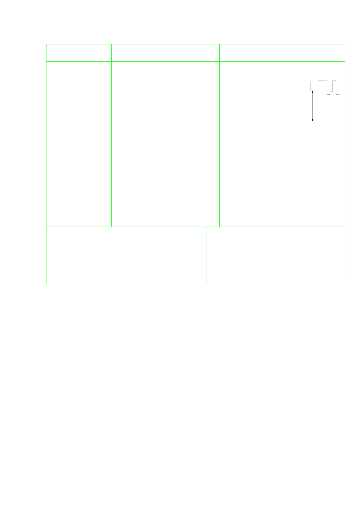
25. VOLTAGE OF
SECOND GRID
OF U
G2
PICTURE TUBE
26. REFERENCE
OSCILLATING
CIRCUIT OF
SOUND
DEMODULATOR
Required instruments:
• oscilloscope,
• oscilloscope probe 100:1;
• Cp=2,5pF (oscilloscope setting
0,5V/div; 5ms/div: ext. actuation
with vertical time b asis of TV set).
Procedure:
• To antenna connector connect signal
with Philips test picture.
• With oscilloscope probe search on
video output stage for the cathode of
picture tube on which video signal
has highest voltage level of black
(oscilloscope setting: 0,5V/div; 20
µs/div: int. triggering). The probe
should remain connected to this
cathode.
• Change the setting o f oscilloscope to
5ms/div and ext. Triggering with
vertical time basis of T V set and on
oscillogram search for measuring
"ABS" impulse (automatic black
point stabilisation).
• To antenna connector of TV
set, which is switched on
and operates in service
mode, connect VF signal
source with PHILIPS test
picture and with 1kHz
modulated sound carrier.
• Connect Volt-meter
• With
potentiometer for
second grid
voltage
adjustment on
HV transformer
set such value of
»ABS« pulse to
voltage 130±2 V.
on pin 5 of IC525.
ABS pulse
0V
• Rotating the core of
L521 coil to set 2,3V
+/-0,lV on Voltmeter.
130V
14
Page 15
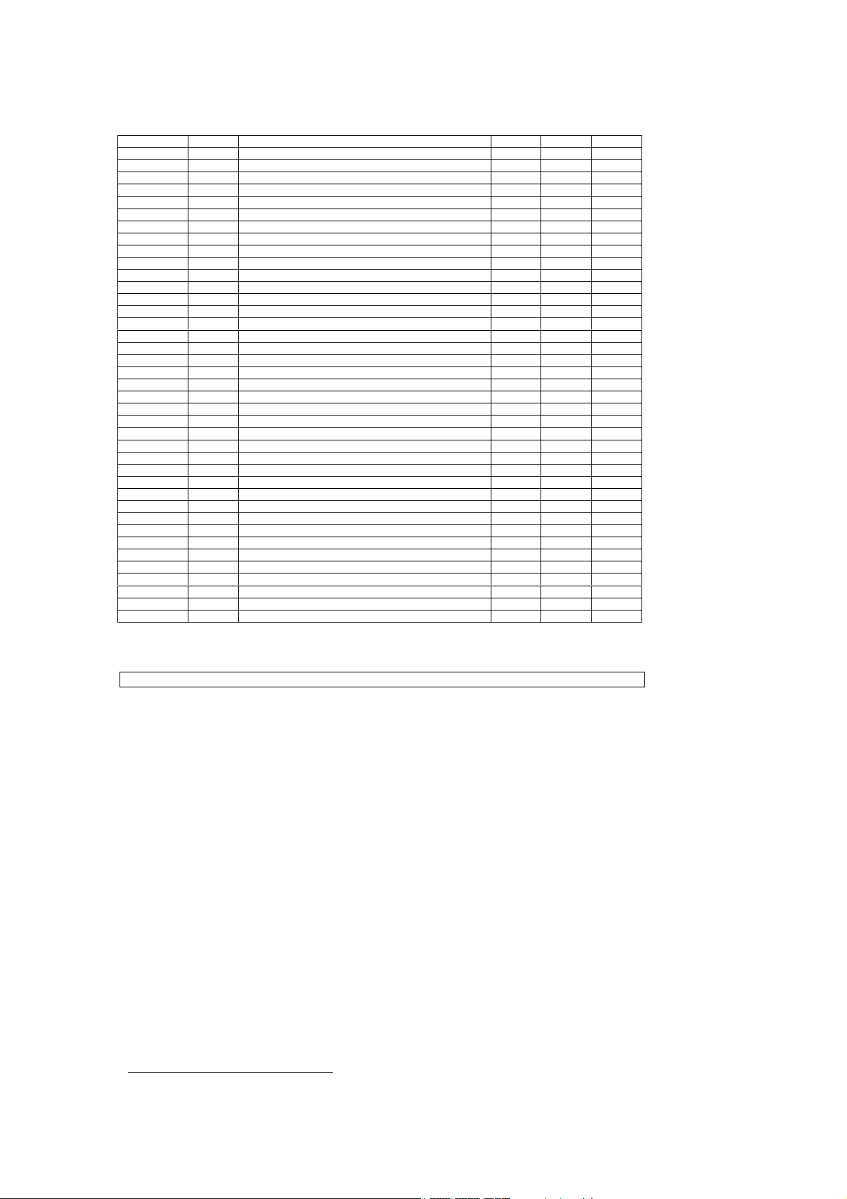
LIST OF SERVICE MODE PARAMETERS
NR. PAR. NAME FUNCTION FW
0 VH Vertical Shift 24h 00h 3fh
1 VA Vertical Amplitude 21h 00h 3fh
2 VS Vertical Slope 25h 00h 3fh
3 SC S-Correction 09h 00h 3fh
4 HS Horizontal Shift 25h 00h 3fh
5 EW EW width 33h 00h 3fh
6 PW EW Parabola/Width 19h 00h 3fh
7 CP EW Corner Parabola 08h 00h 3fh
8 TC EW Trapezium 1fh 00h 3fh
9 EW EW width 33h 00h 3fh
10 X1 Vertical zoom 16:9 (EXREND) 1fh 00h 26h
11 E1 EW width 16:9 (EXTEND) 20h 00h 3fh
12 S1 Vertical Scroll 16:9 (EX TEND ) 20h 00h 3fh
13 P1 PIP horizontal position 20h 00h 7fh
14 PA PIP adjustment right horizontal position 07h 00h 0fh
15 P2 PIP vert ical position 20h 00h 7fh
16 P3 PIP horizontal pos ition - zoom 20h 00h 7fh
17 X2 Vertical zoom CINEMA 00h 00h 26h
18 E2 EW width CINEMA 33h 00h 3fh
19 S2 Vertical Scroll CINEMA 20h 00h 3fh
20 X3 Vertical zoom ZOOM 1ah 00h 26h
21 E3 EW width ZOOM 33h 00h 3fh
22 S3 Vertical Scroll ZOOM 20h 00h 3fh
23 AC AGC take over 07h 00 h 3fh
24 R White point R 1fh 00h 3fh
25 G White point G 24h 00h 3fh
26 B White point B 24h 00h 3fh
27 I1 Adjustment IF-PLL AUTO 40h 00h 7fh
28 I2 Adjustment IF-PLL SECAM L 00h 00h 7fh
29 I3 Adjustment IF-PLL Sound Standard DK 40h 00h 7fh
30 YD Y-Delay 0dh 00h 0fh
31 HM Hotel Mode Max Loudspeaker value 2fh 00h 7fh
32 HD Display Ho r iz o nt al Delay 10h 00h 1fh
33 RG RGB Ga in for OSD 02h 00h 03h
34 O1 Option byte 1 20h 00h ffh
35 O2 Option byte 2 02h 00h ffh
36 O3 Option byte 3 50h 00h ffh
37 O4 Option byte 4 00h 00h ffh
38 O5 Option byte 5 00h 00h ffh
1
MIN MAX
FATAL ERROR DETECTION
VIDEO PROCESSOR NOT DETECTED, or POWER UP RESET o f Video Processor not finished – LED flashing with 1Hz.
1
Firmware value – Used in case of empty EEPROM or on service table checksum fail
15
Page 16
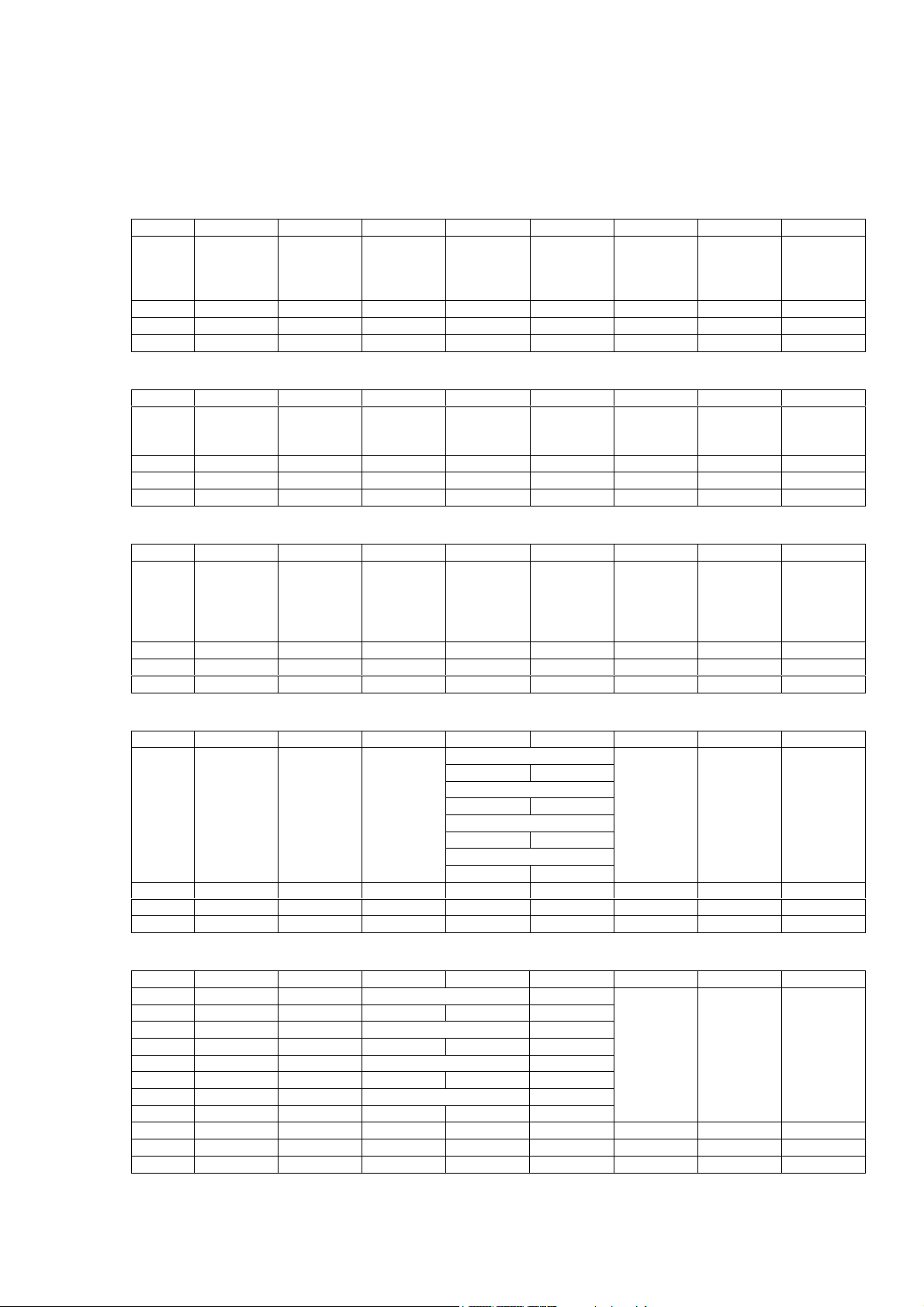
OPTION BYTES
Option bytes enable programme configuration of colour TV set. Changing individual bites of a
byte modifies the characteristics of TV set.
Option byte O1:
Position76543210
Slo
language
1 Enable Enable Enable Enable Enable 123 degrees Enable Enable
0 Disable Disable Disable Disable Disable 118 degrees Disable Disable
FW00100000
Hotel mode Black
stretch
Blue stretch Dynamic
skin control
Dynamic
skin
correction
angle
Blue back NTSC
Option Byte O2:
Position76543210
Headphone
menu
1 Disable 38 Enable Enable Enable Disable Enable Enable
0 Enable 06 Disable Disable Disable Enable Disable Disable
FW00000010
User set
(east or
west)
Top TV set is
16:9
EEPROM
language
HBL bit
video proc.
On 4:3
Multistanda
rd TV
PAL I
Option Byte O3:
Position76543210
Italian
channels
(c13-c20)
1 Disable Disable Enable Enable Standard Enable Enable
0 Enable Enable Disable Disable Delayed 8s Disable Disable
FW01010000
Zoom on
4:3
HBL in
TXT (110
chassis)
Avl (90
chassis)
AVL option Switch on ROM
language
Not used CTI
Option Byte O4:
Position76543210
Force
mono
volume
1 Enable Enable Enable Enable Enable Enable
0 Disable Disable Disable Disable Disable Disable
FW000000 0
DCO
adjustment
and
INDIA_TV
DK toggle
alternate
sound (red
key)
6.5Mhz and
5.74Mhz to
6.25 and
5.74 Mhz
Space effect
00
3D effect
01
Virtual Dolby effect
10
Virtual Dolby (text 3D)
11
Zet
correction
Auto on
(for quality
department)
Low
standby
Option Byte O5:
Position76543210
Not used Not used Tuner Scan 1 x 4 Not used
00
Tuner Scan Reverse U x 6
01
Tuner Scan 3 x 3
10
Tuner Scan 3 x 4
11
1 Enable Enable Enable
0 Disable Disable Disable
FW00000000
Second
zoom
(UK)
Tuner scan Equaliser
16
Page 17
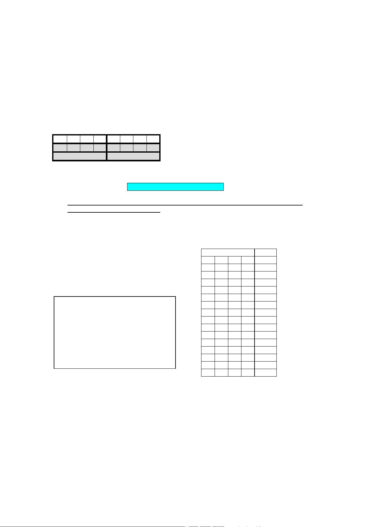
Option bytes are set so that besides selected op tion byte also hexad ecimal number is set on th e basis of
above tables.
Example:
• blue back-enable
• dynamic skin control enable
• blue stretch enable
Select option byte O1 and for items, which should be activated, set “1” (other bites are “0”). In our case
is as follows:
O1:
76543210
0 0 0 1 1 0 1 0
1 A
Shaded binary number should now be converted to hexadecimal value (darker frame). Afterwards set
this value.
SERVICE PARAM: O1 VALUE: 1A
• CAUTION: Option bytes are Factory adjusted and must NOT be changed later, because
they change TV set characteristics.
27. INFORMATION MENU ABOUT
INTEGRATED CIRCUITS,
CONNECTED TO I
2
C-BUS
If you press i key (info) on remote control
when the TV set is in service mode, you will
get on the screen information about
of current software (e.g.: VER: E9P7 4.5) and
the version
devices connected on I2C bus:
SERVICE
E9P7 4.5
TDA8843
MSP 34XX OK WD: FF
SDA9488 XX SP : 00
TUNER2 XX
TDA 8540 XX
TDA8425 X
Video processor: Bus controlled TV processor
for video and audio signal
MSP 34XX: Digital stereo sound
processor
If device is installed and properly connected on
I2C bus it will respond with “OK” beside the
name of device, otherwise there will be “XX”
on this place.
For conversion from binary to hexadecimal
help us next table:
BIN HEX
0000 0
0001 1
0010 2
0011 3
0100 4
0101 5
0110 6
0111 7
1000 8
1001 9
1010 A
1011 B
1100 C
1101 D
1110 E
1111 F
17
Page 18
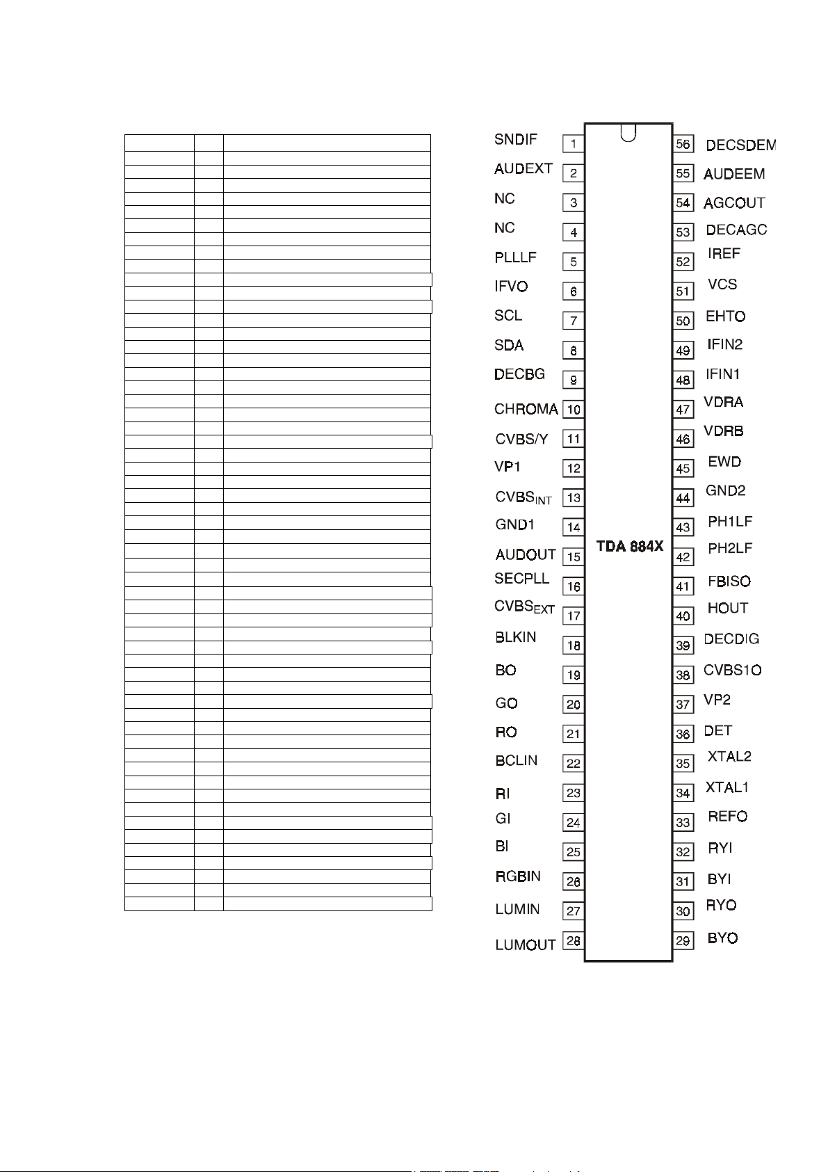
IC PIN DETAILS
TDA8843
SYMBOL PIN DESCRIPTION
SNDIF 1 Sound IF input
AUDIOEXT 2 External audio input
NC 3 not connected
NC 4 not connected
PLLLF 5 IF-PLL loop filter
IFVO 6 IF video output
SCL 7 serial clock input
SDA 8 serial data input/output
DECBG 9 bandgap decoupling
CHROMA 10 chrominance input (S-VHS)
CVBS/Y 11 external CVBS/Y input
VP1 12 main supply voltage 1 (+8V)
CVBS
GND1 14 ground1
AUDIOOUT 15 audio output
SECPLL 16 SECAM PLL decoupling
CVBS
BLKIN 18 black-current input
BO 19 blue output
GO 20 green output
RO 21 red output
BCLIN 22 beam current limiter input/V-guard input
RI 23 red input for insertion
GI 24 green input for insertion
BI 25 blue input for insertion
RGBIN 26 RGB insertion input
LUMIN 27 luminance input
LUMOUT 28 luminance output
BYO 29
RYO 30
BYI 31
RYI 32
REFO 33 subcarrier reference output
XTAL1 34 3.58MHz crystal connection
XTAL2 35 4.43/3.58MHz crystal connection
DET 36 loop filter phase detector
VP2 37 2nd supply voltage 1(+8V)
CVBS1O 38 CVBS-1 output
DECDIG 39 Decoupling digital supply
HOUT 40 horizontal output
FBISO 41 flyback input/sandcastle output
PH2LF 42 phase-2 filter
PH1LF 43 phase-1 filter
GND2 44 ground 2
EWD 45 east-west drive output
VDRB 46 vertical driveB output
VDRA 47 vertical driveA output
IFIN1 48 IF input 1
IFIN2 49 IF input 2
EHTO 50 EHT/overvoltage protection input
VSC 51 vertical sawtooth capacitor
IREF 52 reference current input
DECAGC 53 AGC decoupling capacitor
AGCOUT 54 tuner AGC output
AUDEEM 55 Audio deemphasis
DECSDEM 56 Decoupling sound demodulator
13 internal CVBS input
INT
17 external CVBS input
EXT
(B−Y) signal output
(R−Y) signal output
(B−Y) signal input
(R−Y) signal input
18
Page 19
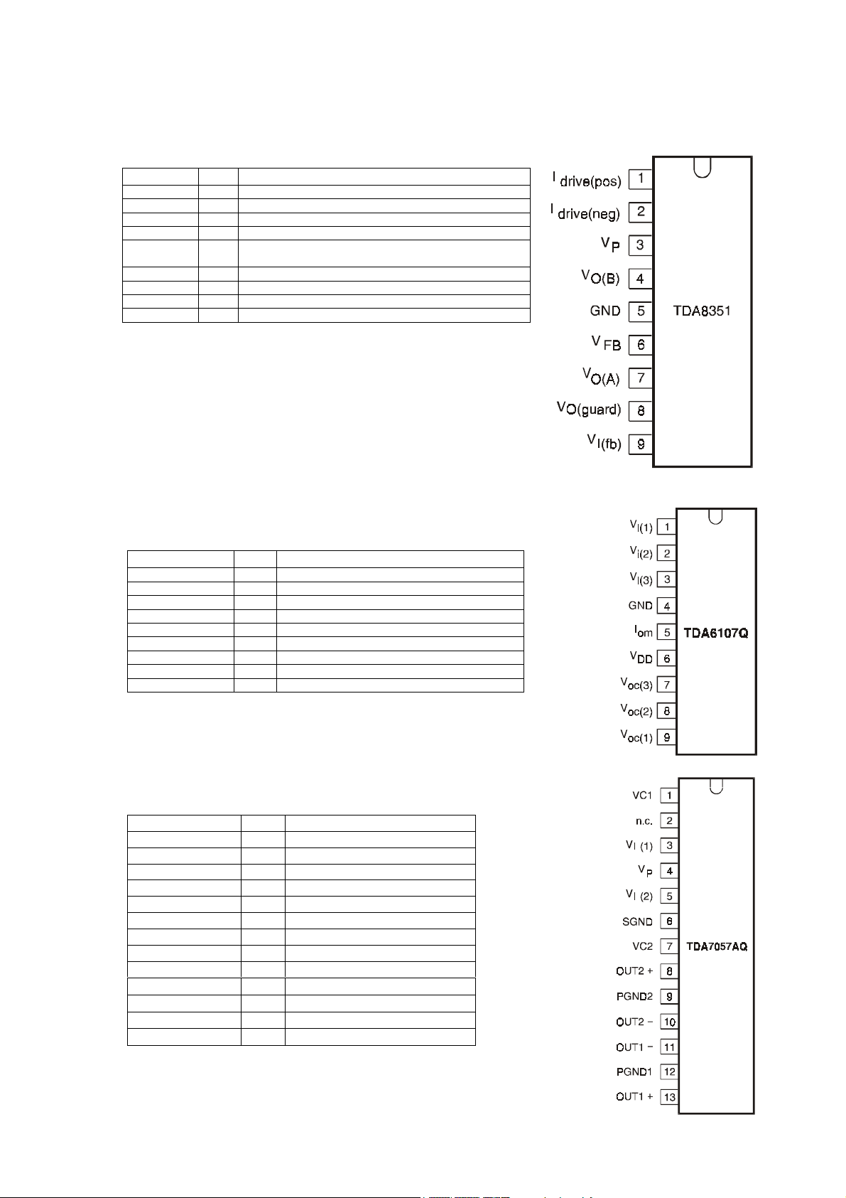
TDA8351
SYMBOL PIN DESCRIPTION
I
drive(pos)
I
drive(neg)
V
P
GND 5 ground
1 input power-stage (positive);
2 input power-stage (negative);
3 operating supply voltage VO(B)
4 output voltage B
includes I
I(sb) signal bias
includes I
I(sb) signal bias
V
FB
V
O(guard)
V
I(fb)
6 input flyback supply voltage VO(A)
7 output voltage A
8 guard output voltage VI(fb)
9 input feedback voltage
TDA6107Q
SYMBOL PIN DESCRIPTION
Vi(1) 1 inverting input 1
Vi(2) 2 inverting input 2
Vi(3) 3 inverting input 3
GND 4 ground (fin)
Iom 5 black-current measurement output
V
DD
Voc(3) 7 cathode output3
Voc(2) 8 cathode output2
Voc(1) 9 cathode output1
6 supply voltage
TDA7057Q
SYMBOL PIN DESCRIPTION
VC1 1 DC volume control1
n.c. 2 not connected
V
l (1)
V
P
V
l (2)
SGND 6 signal ground
VC2 7 DC volume control2
OUT2+ 8 positive output2
PGND2 9 power ground2
OUT2−
OUT1−
PGND1 12 power ground1
OUT1+
3 voltage input1
4 positive supply voltage
5 voltage input2
10 negative output2
11 negative output1
13 positive output1
19
Page 20
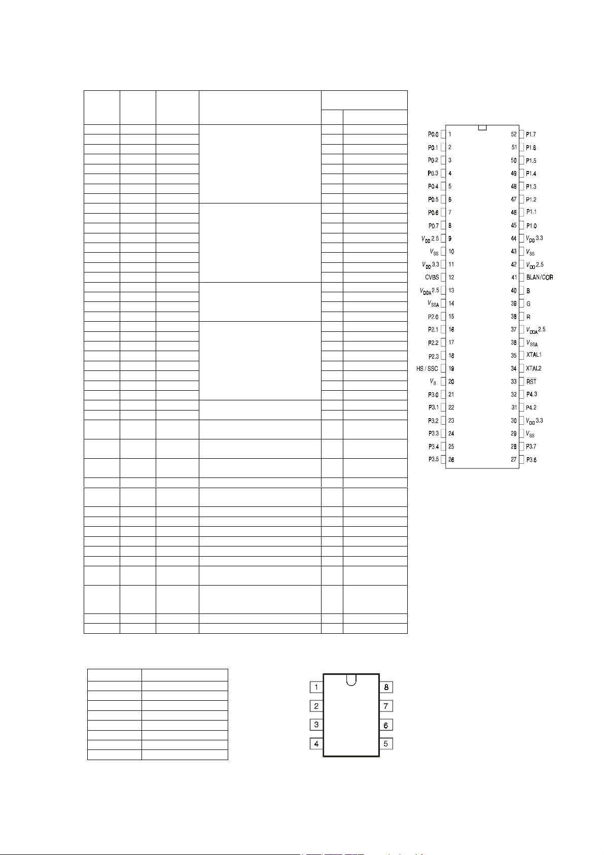
SDA5553-A009/EV E945
F
Input (I)
Symbol
P0.0 1 I/O O AV/TV
P0.1 2 I/O O BG/L
P0.2 3 I/O O DECODER
P0.3 4 I/O O BL_SC1
P0.4 5 I/O I/O IIC-SDA
P0.5 6 I/O I/O IIC-SCL
P0.6 7 I/O I/O IIC-SDA
P0.7 8 I/O
P1.0 45 I/O O L/L'
P1.1 46 I/O O LED
P1.2 47 I/O I/O N.C. (h)
P1.3 48 I/O I/O COPY
P1.4 49 I/O I/O BG/DK
P1.5 50 I/O O SVHS_COMB
P1.6 51 I/O O VOL
P1.7 52 I/O
P2.0 15 I I KEYB
P2.1 16 I I PERI1
P2.2 17 I I PERI2
P2.3 18 I
P3.0 21 I/O O ON/OFF
P3.1 22 I/O O TxD
P3.2 23 I/O I/O SCART1/2
P3.3 24 I/O I RC5
P3.4 25 I/O I/O BG/L_PIP
P3.5 26 I/O I/O AV1/AV2_PIP
P3.6 27 I/O O MSP_RESET
P3.7 28 I/O
P4.2 31 I/O I TUN_SELECT1
P4.3 32 I/O
XTAL2 34 O
XTAL1 35 I
RESET 33 I
V
DD
V
DDA
V
DD
V
SS
V
SSA
R 38 O Red colour signal output
G 39 O Green colour signal output
B 40 O Blue colour signal output
BLANK/
COR
HS/SSC 19 I
V
S
CVBS 12 I CVBS (video signal) input
Pin No.
2.5
2.5
3.3
11,30,47 S Power supply voltage
10,29,43 S Ground (0 V)
Output (O)
Supply (S)
Port 0 is an 8-bit open drain
bi-directional I/O port. Port 0 pins
that have 1s written to them
float; in this state they can be
used as high-impedance inputs
(e.g. for software driven
Bus).
Port 1 is an 8-bit bi-directional
multifunctional I/O port with
internal pull-up resistors.
Port 2 is a 4-bit input port without
pull-up resistors. Port 2 also
works as analogue input for the
4-channel-ADC.
Port 3 is an 8-bit bi-directional
I/O port with internal pull-up
resistors.
Port 4 is a bi-directional I/O
port
Output of the inverting oscillator
amplifier.
Input to the inverting oscillator
amplifier
A low level on this pin resets the
9, 42 S Power supply voltage for RGB
13, 37 S
14, 36 S Ground (0 V) for Slicer and ADC
41 O
20 I/O Vertical sync input for display
processor
Power supply voltage for Slicer
and ADC
Blanking output/ Contrast
Reduction output
Horizontal sync input (alternative
sandcastle sync input) for
display
Function
2
I
C
EV PINING
UNCTION
I/0
1
1
I/O IIC-SCL
I/O Z_COR
I ADC3
IRxD
I TUN_SELECT2
2
2
SDA5553
24C16
Pin No. Function
1 Internal N.C.
2 Internal N.C.
3 Internal N.C.
4 Ground
5 Seral Adress/Data
6 Serial Clock
7 Write Protect Input
8 Supply voltage input
A1
A2
VSS
A0
24C16
VCC
WP
SCL
SDA
20
Page 21
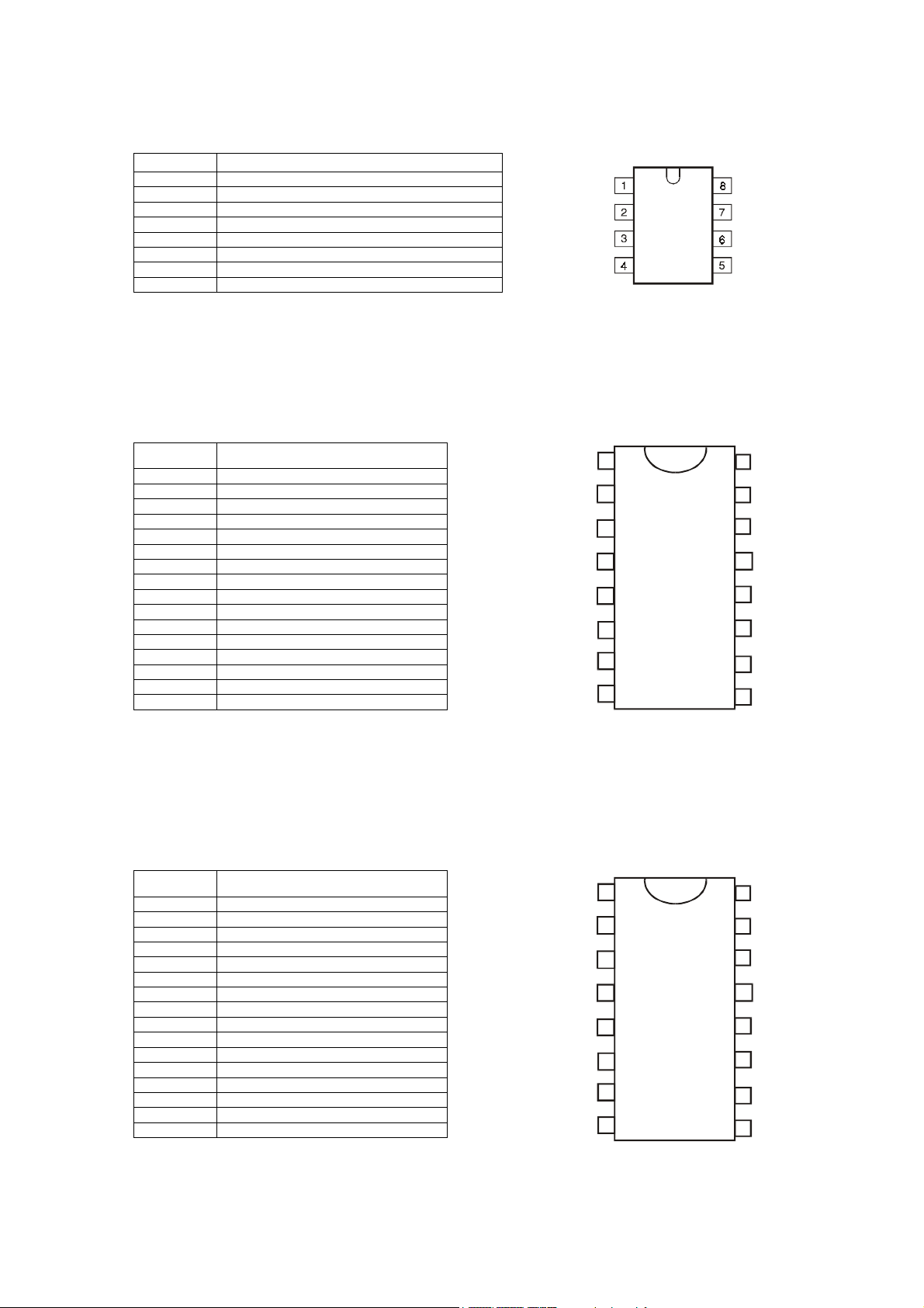
TDA4605-2
Pin No. Function
1 Information Input Concerning Secondary Voltage
2 Information Input Regarding the Primary Current
3 Input for Primary Voltage Monitoring
4 Ground
5 Output
6 Supply Voltage Input
7 Input for Soft-Start and Integrator Circuit
8 Input for the Feedback of the Oscillator
U4468B
Pin No. Function
1 `IF` input
2 `IF` input
3 Capacitor for AGC` time constant
4 Capacitor for internal reference voltage
5 Loop filter
6 A.F. output (AM sound)
7 Standard switch
8 Reference VCO L.C. network
9 Reference VCO L.C. network
10 AM mute switch
11 not connected
12 Sound IF output (FM` sound)
13 Ground
14 Supply voltage 5V
15 not connected
16 not connected
V
sw,AGC
V
V
V
C
C
LF
V
o,AM
VCO
U_R
U_PIS
U_PUD
GND
i,IF
i,IF
AGC
REF
1
2
3
4
5
6
7
8
TDA4605-2
U4468B
U_ZCD
U_SST
U_S
OUT
16
n.c.
15
n.c.
14
V
13
GND
12
V
11
n.c.
10
V
V
9
s
o,FM
sw,mute
VCO
TDA4445B
Pin No. Function
1 `IF` input
2 not connected
3 IF `AGC` time constant
4 not connected
5 Average capacitor
6 A.F. output (AM sound)
7 not connected
8 Reference L.C. network
9 Reference L.C. network
10 not connected
11 Supply voltage 12V
12 Sound IF output (FM` sound)
13 Ground
14 not connected
15 not connected
16 `IF` input
C
V
V
V
i,IF
n.c.
AGC
n.c.
C
av
o,AM
n.c.
VCO
1
2
3
4
5
6
7
8
16
15
14
13
12
11
10
9
V
i,IF
n.c.
n.c.
GND
V
o,FM
V
s
n.c.
V
VCO
21
Page 22
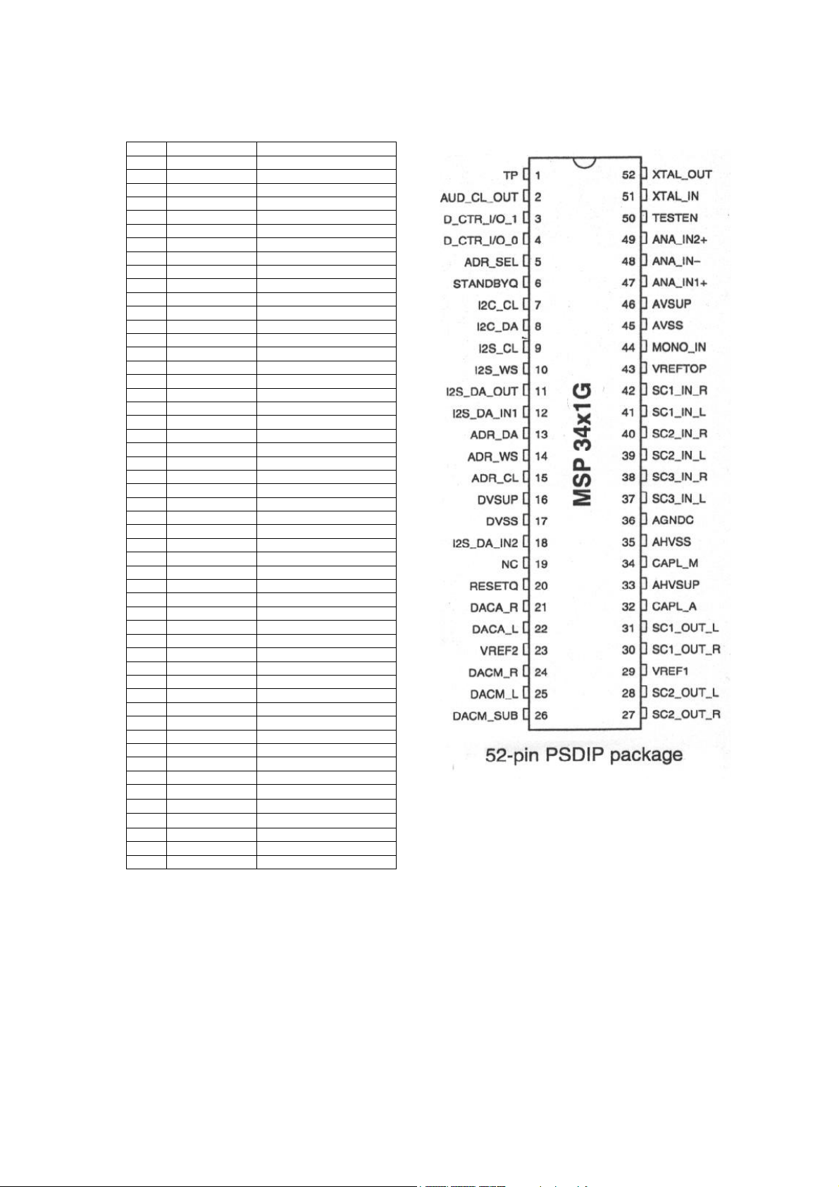
MSP3411G (MSP3401G, MSP3405G, MSP3415G)
PIN Pin Name Short Description
1 TP Test pin
2 AUD_CL_OUT Audio clock output
3 D_CTR_I/O_1 D_CTR_I/O_1
4 D_CTR_I/O_0 D_CTR_I/O_0
5 ADR_SEL I2C Bus address select
6 STANDBYQ Stand-by (low-active)
7 I2C_CL I2C clock
8 I2C_DA I2C data
9 I2S_CL I2S clock
10 I2S_WS I2S word strobe
11 I2S_DA_OUT I2S data output
12 I2S_DA_IN1 I2S1 data input
13 ADR_DA ADR data output
14 ADR_WS ADR word strobe
15 ADR_CL ADR clock
16 DVSUP Digital power supply 5 V
17 DVSS Digital ground
18 I2S_DA_IN2 I2S2-data input
19 NC Not connected
20 RESETQ Power-on-reset
21 DACA_R Headphone out, right
22 DACA_L Headphone out, left
23 VREF2 Reference ground 2
24 DACM_R Loudspeaker out, right
25 DACM_L Loudspeaker out, left
26 DACM_SUB Subwoofer output
27 SC2_OUT_R SCART output 2, right
28 SC2_OUT_L SCART output 2, left
29 VREF1 Reference ground 1
30 SC1_OUT_R SCART output 1, right
31 SC1_OUT_L SCART output 1, left
32 CAPL_A Volume capacitor AUX
33 AHVSUP Analog power supply 8 V
34 CAPL_M Volume capacitor MAIN
35 AHVSS Analog ground
36 AGNDC Analog reference voltage
37 SC3_IN_L SCART 3 input, left
38 SC3_IN_R SCART 3 input, right
39 SC2_IN_L SCART 2 input, left
40 SC2_IN_R SCART 2 input, right
41 SC1_IN_L SCART 1 input, left
42 SC1_IN_R SCART 1 input, right
43 VREFTOP Reference voltage IF
44 MONO_IN Mono input
45 AVSS Analog ground
46 AVSUP Analog power supply 5 V
47
ANA_IN1
48
49
50 TESTEN Test pin
51 XTAL_IN Crystal oscillator
52 XTAL_OUT Crystal oscillator
ANA_IN
ANA_IN2
−
+
+
IF input 1
IF common
IF input 2
22
Page 23
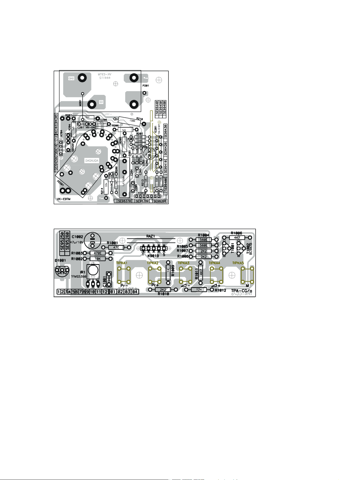
PCB LAYOUTS
VK-E9TM
TPA-CG
23
Page 24
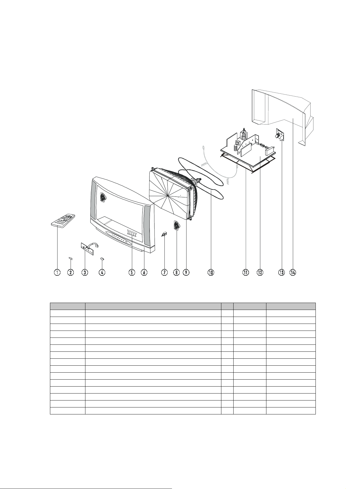
EXPLODED VIEW S28AG/S 12S0
Pos. On Pict. Description Qty Ident.Nr. Code
--EXPLODED VIEW – DR AWING--
1 REMOTE HANDSET PR 108
2 IR, LED GLASS 1 431976
3 MODULE TPA-CG SE 95250 1 441159
4 BUTTON FOR MAIN SWITCH 1 439334
5 BUTTONS UE 1 439334
6 HOUSING S28“ SI 1 444455
7 MAIN SWITCH 1 438101
8 LOUDSPEAKER 8Ω 15W 2 420717
9 COLOUR PICTURE TUBE A 66 EHJ 1 438152
10 DEGAUSSING COIL 28“ 1 444802,444765
11 CHASSIS FRAME 1 444849
12 MAIN CHASSIS 12 P/I N (S.B. = 20-81-40-00-00) 1 443006
13 MODULE VK-E9 SE 96320 1 441651
14 BACK COVER 28“ SI 1 437085
GRUNDIG
1 441838
1 444872
24
Page 25

LIST OF RECOMMENDED SPARE PARTS FOR CHASSIS AND MODULES
CODE VALUE POSITION
MAIN CHASSIS
412499 C/EL 220U M400V C-12642
415949 C/EL PR 5,0 2U2 M350V C-12709 5,0
338557 C/EL PR 5,0 10U T250V C-12606 5,0
414794 C/EL PR 5,0 47U M160V C-12605 5,0
415947 C/EL TR 5,0 1U0 M250V C-12714 5,0
412517 C/CE/Y/2E4/Z NR12,5 2N2M400VAC C-12645
413778 CMPP 22,5 U33 J 250V C-12707
413782 C/MPP PR * U68 M 250V C-12715
338584 C/PP 22,5 U011 J 1,6KV C-12711 22,5
338585 C/PP 22,5 U033 J 1KV C-12713 22,5
415936 C/PP PR * U033 K 630V C-12627
415937 C/PP PR15,0 220P J 1,6KV C-12625 15,0
429609 C/X2 PR* U47 M 275VAC C-12641
429610 C/X2 U10 M 275VAC C-12646 15,0
429611 C/X2 U22 M 275VAC C-12636 22,5
313551 D/SI/1N4001 TA D-12701 12,5
313551 D/SI/1N4001 TA D-12702 12,5
51666 D/SI/1N4148 TA D-12104 10,0
51666 D/SI/1N4148 TA D-12106 10,0
51666 D/SI/1N4148 TA D-12109 12,5
51666 D/SI/1N4148 TA D-12601 12,5
51666 D/SI/1N4148 TA D-12606 12,5
51666 D/SI/1N4148 TA D-12705 12,5
51666 D/SI/1N4148 TA D-12710 12,5
412464 D/SI/BAT85 D-12108 17,5
324669 D/SI/BY228 TA D-12706 20,0/H10
410680 D/SI/BYW74 TA D-12708 20,0/H10
410680 D/SI/BYW74 TA D-12607 15,0/H10
410680 D/SI/BYW74 TA D-12609 15,0/H10
410680 D/SI/BYW74 TA D-12614 15,0/H10
424580 D/SI/BYT52G D-12302 12,5
424580 D/SI/BYT52G D-12604 12,5
424580 D/SI/BYT52G D-12703 12,5
424580 D/SI/BYT52G D-12704 12,5
424580 D/SI/BYT52G D-12709 12,5
424279 D/SI/BYT52M TA D-12608 12,5
415931 D/SI/BYW54 TA D-12610 12,5
415931 D/SI/BYW54 TA D-12611 12,5
415931 D/SI/BYW54 TA D-12612 12,5
415931 D/SI/BYW54 TA D-12613 12,5
417320 D/SI/BYW95C TA D-12602 15,0/H10
417320 D/SI/BYW95C TA D-12707 15,0/H5
68571 DIODE Z/ 2,7V/C/0,5W D-12711 10,0
304326 DIODE Z/33 V/C/0,5W TA D-12603 12,5
435879 MAINS CHOKE 2X70 mH DU-12602
439745 IC SDA5553-A009/EV E945 IC-12001
429960 IC AT24C08-10PC IC-12002
25
Page 26

CODE VALUE POSITION
MAIN CHASSIS
415922 IC LM317T IC-12004, IC-12005
415922 IC LM317T IC-12602, IC-12604
427444 IC TDA8843/N2C IC-12101
419821 IC TDA7057AQ IC-12102
366430 IC TEA2014 IC-12104
425757 IC TDA8351 IC-12301
438568 IC U4468B IC-12501
430973 IC MSP3415G PSDIP52 IC-12503
415921 IC TDA4605-2 IC-12601
415923 IC MC7808T IC-12603
419715 IC 74HCT4053 IC-12801
444164 TUNER TEDE9-226A TUN-12101
68503 IC SOCKET 8 FOR IC-12002
426141 HEADER 7/2,5 K-12102A
426141 HEADER 7/2,5 K-12901A
423427 CONNECTOR M/ / 4/2,5 MKS1954 K-12701
424019 CONNECTOR M/ 3/2,5 90647-1003 K-12301A
423988 CONNECTOR M/ 4/2,5 90647-1004 K-12702A
423989 CONNECTOR M/ 5/2,5 90647-1005 K-12104A
319045 CRYSTAL 4,4 MHz Q-12101
431081 CRYSTAL 6 MHz Q-12001
439430 CRYSTAL 18,432 MHZ Q-12501
316831 FUSE HOLDER FOR VA-12601
316831 FUSE HOLDER FOR VA-12602
316831 FUSE HOLDER FOR VA-12603
421055 METAL SHIELD EMC E6/E7 MP-12101
79039 PASTE SILICON P12 FOR HEATSINK T-12705
410208 MICA WASHER FOR IC-12602
410208 MICA WASHER FOR IC-12604
338708 MICA WASHER FOR T-12602
338569 R/PL TA R47 J 0,5 W R-12703 15,0
415965 R/PL TA 5K1 J 0,33 W R-12610 10,0
433775 R/MF 220K J 3,5kV R-12615 12,5
372123 R/FUSIBLE TA 2R2 J 0,33W R-12156 15,0/H10
372123 R/FUSIBLE TA 2R2 J 0,33W R-12715 15,0/H10
411573 R/FUSIBLE R39 K 0,75W R-12140 15,0/H10
421131 R/FUSIBLE TA 47R J 0,33W R-12304 20,0/H10
421131 R/FUSIBLE TA 47R J 0,33W R-12609 15,0/H10
415009 R/FUSIBLE TA 1K J 0,5 W R-12707 15,0/H10
411572 R/FUSIBLE TA R15 K 0,75W R-12622 15,0/H10
411574 R/FUSIBLE TA R22 K 0,4 W R-12710 15,0/H15
411574 R/FUSIBLE TA R22 K 0,4 W R-12713 15,0/H15
419823 R/PLK 0204 TA 2K05 F 0,25 W R-12618 12,5
69833 R/CL 0204 TA 8K2 J 0,33 W R-12118 10,0
330380 R/PLK 0204 TA 3K F 0,25 W R-12308 12,5
429553 R/PLK 0204 TA 39K F 0,25 W R-12122 12,5
419824 R/PLK 0204 TA 243R F 0,25 W R-12052, R-12044 10,0
419824 R/PLK 0204 TA 243R F 0,25 W R-12616, R-12623 12,5
419825 R/PLK 0204 TA 715R F 0,25 W R-12625 12,5
416940 R/HV TA 220K J 1 kV R-12701 12,5
26
Page 27

CODE VALUE POSITION
MAIN CHASSIS
433776 R/HV TA 820K J 1,6KV R-12613 12,5
420920 R/MOX TA 1R0 J 1W R-12306 20,0/H10
316701 R/PLKO TA R82 J 1 W R-12702 15,0
429521 R/PLKO TA 2R7 J 4 W R-12714 20,0/H15
419822 R/PLKO TA 10R J 2 W R-12725 20,0/H20
416508 R/PLKO TA 22K J 2 W R-12603 20,0/H15
415953 R/PLKO TA 27K K 4 W R-12624 35,0/H20
415952 R/PLKO TA 47K J 1,5 W R-12606 20,0/H10
429522 R/PLKO TA 75K J 4 W R-12604 20,0/H15
316651 R/MOX TA 180R K 1,5W R-12305 20,0/H10
68544 R/PTC - DEGAUSSING R-12628
338709 CLIP IC FOR IC-12102, IC-12301
338709 CLIP IC FOR IC-12602, IC-12604
338709 CLIP IC FOR T-12602, T-12701
422699 CLIP IC FOR T-12705
423137 T/FET/BUZ90A T-12602
338580 T/NPN/AF/BC639 TR T-12703
411262 T/NPN/BC547B TR T-12003, T-12004, T-12005
411262 T/NPN/BC547B TR T-12006, T-12007, T-12009
411262 T/NPN/BC547B TR T-12010, T-12104, T-12105
411262 T/NPN/BC547B TR T-12108, T-12501, T-12601
411262 T/NPN/BC547B TR T-12603, T-12702, T-12706
415900 T/NPN/BU508AF T-12701
415928 T/NPN/PH2369 TR T-12008, T-12109
415928 T/NPN/PH2369 TR T-12801, T-12802
411261 T/PNP/BC212B/BC557B TR T-12107, T-12110, T-12704
414036 T/PNP/BD242 T-12705
425763 TRANSFORM. SMPS E9 110 TR-12601
435877 TRANSFORM.HV E9 TR-12701
378773 TRANSFORM. DRIVER TR-12702
339150 LINEARITY COIL 12-25 L-12701
420742 COIL 550UH L-12703
437560 POWER FACTOR CORRECTION COIL PFC
21108 FUSE T 1,25 A L 250V VA-12601, VA-12602
431998 FUSE T 2 A E 250V VA-12603
MODULES
MODULE VK-E9TM
415032 C/EL 5,0 2U2 M250V C-9202 5,0
300874 D/SI/1N4003 TA D-9205 12,5
425755 IC TDA6107Q IC-9201
435872 CRT SOCKET B10-277 0330 550034 PD-9201
411567 R/FUSIBLE TA 120R J 0,75W R-9210 20,0/H10
339317 R/CL TA 2R2 J 1,5W R-9207 20,0/H10
338709 CLIP IC FOR IC-9201
426035 VARISTOR 35V VAR-9201
MODULE TPA-CG
425987 IC TSOP IR-91001
420171 D/LED R/G D-91001
411262 T/NPN/BC547B TR T-91001, T-91002
441536 FUNCTION KEY TI-1…TI-5
27
Page 28
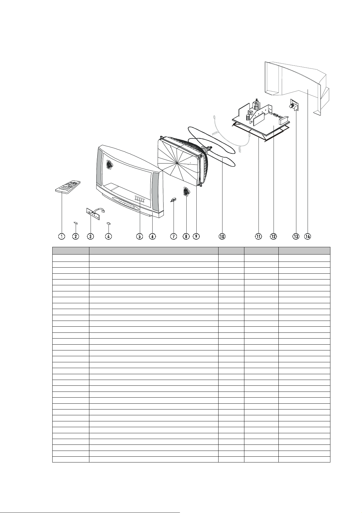
MANUFACTURING PARTS FOR TV S28AG/S 12S0
Pos. On Pict. Description Qty(pcs) Ident.Nr. Code
--EXPLODED VIEW – DR AWING--
1 REMOTE HANDSET PR 108 GRUNDIG 1 444872
2 IR, LED GLASS 1 431976
3 MODULE TPA-CG SE 95250 1 441159
4 BUTTON FOR MAIN SWITCH 1 439334
5 BUTTONS UE 1 439334
6 HOUSING S28“ SI 1 444455
7 MAIN SWITCH 1 438101
8 LOUDSPEAKER 8Ω 15W 2 420717
9 COLOUR PICTURE TUBE A 66 EHJ 1 438152
10 DEGAUSSING COIL 28“ 1 444802,444765
11 CHASSIS FRAME 1 444849
12 MAIN CHASSIS 12 P/I N (S.B. = 20-81-40-00-00) 1 443006
13 MODULE VK-E9 SE 96320 1 441651
14 BACK COVER 28“ SI 1 437085
User manuals 2 444957 & 444958
Battery R6S 2 422401
Designation relief “GRUNDIG” 1 438887
SCREW A 2,9X9,5 for main sw. & mod. TPA-CG 4 18149
SCREW A 3,9X9,5 for back cover 1 89338
SCREW A 5,5X44 for back cover 2 421535
SCREW A 3,5X16 for back cover 4 435136
SCREW B 7X32 for picture tube 4 420407
SCREW A 3,5X9,5 for loudspeakers 8 26495
Distance holder 28” 4 427206
Washer for picture tube 4 439451
Chassis holder 16:9 28” 1 428634
CRT carrier 2 431984
CABLE for loudspeakers 1 436596
CABLE for defl. yokes 1 436766
Soldering wire 1,5 1,6g 26575
Cartoon box with packaging 1 444454 & 444453
Spring for mains button 1 431975
Driller with base 1 77578
Spec clean. agent 1ml 378986
1 441838
28
Page 29
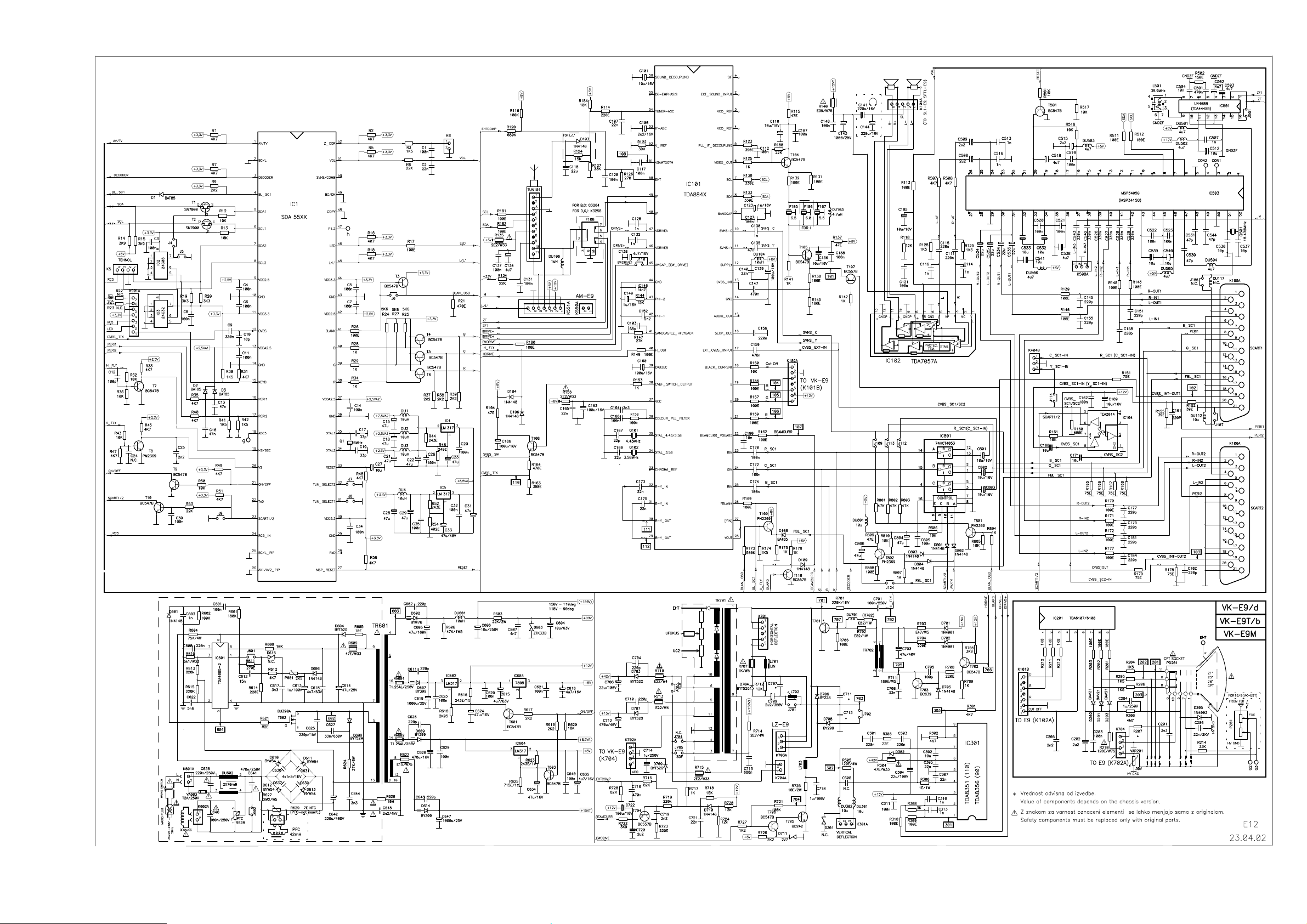
CIRCUIT DIAGRAM OF MAIN CHASSIS E12
29
Page 30
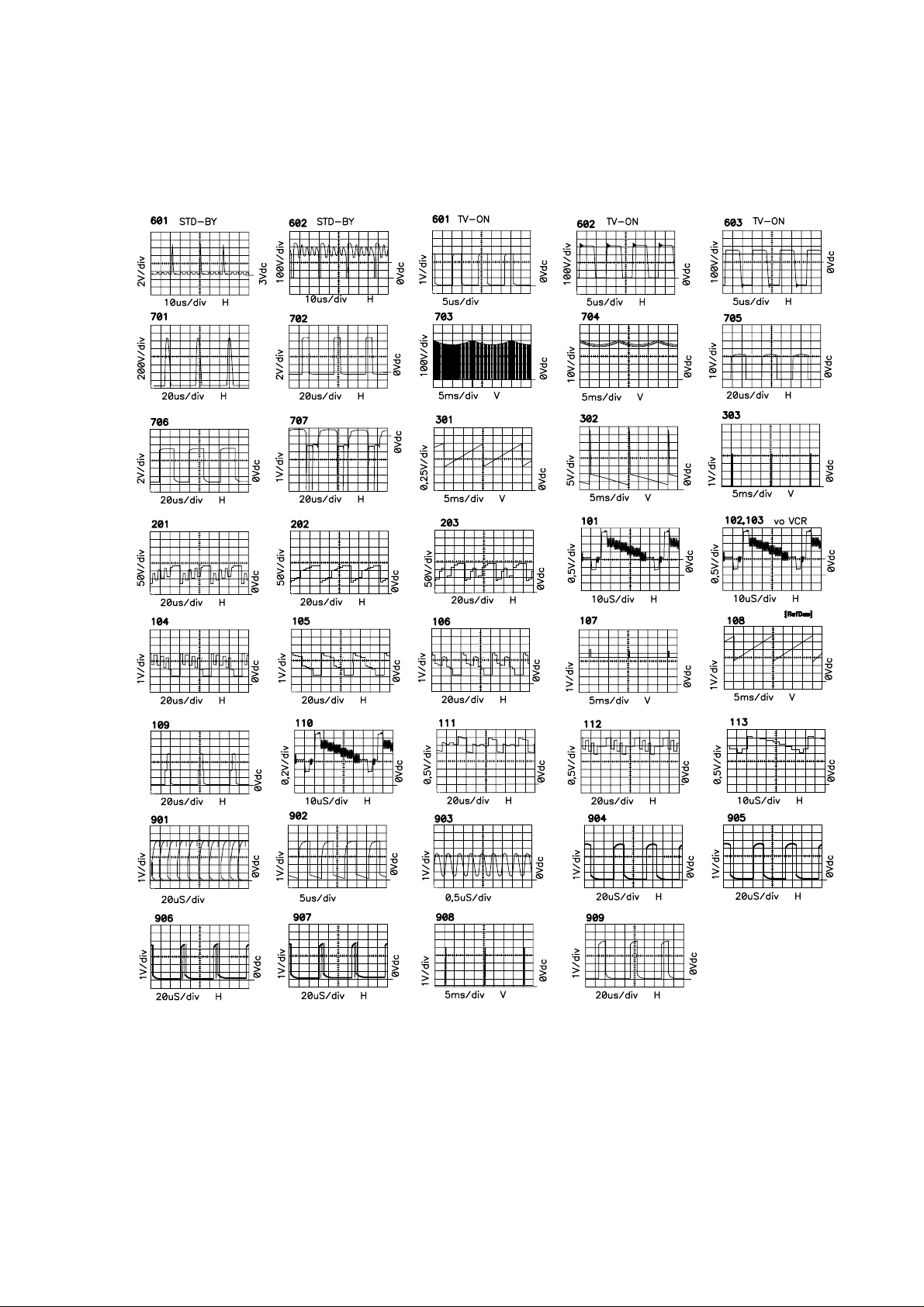
OSCILLOGRAMS
30
Page 31
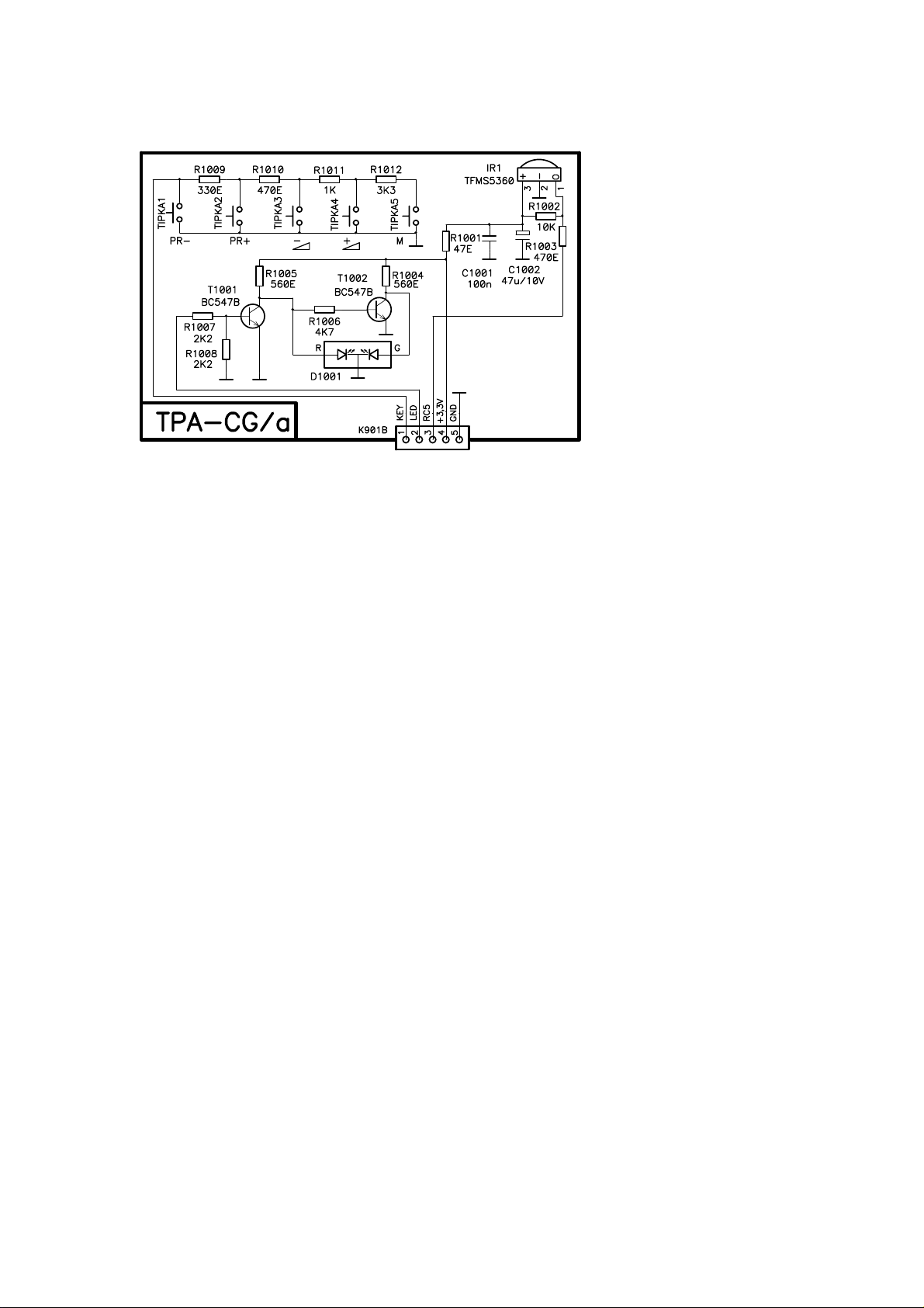
ELECTRICAL DIAGRAMS OF SEPARATE MODULES OF CHASSIS E12
NOTES:
31
 Loading...