

Page 1

This file is provided FREE OF CHARGE from the
electromaniacs.com community
You are free to distribute this file to other persons
who needs it , but without of charge
Also on
thousands of service manuals , schematics free of
charge
http://electromaniacs.com you can find
Page 2
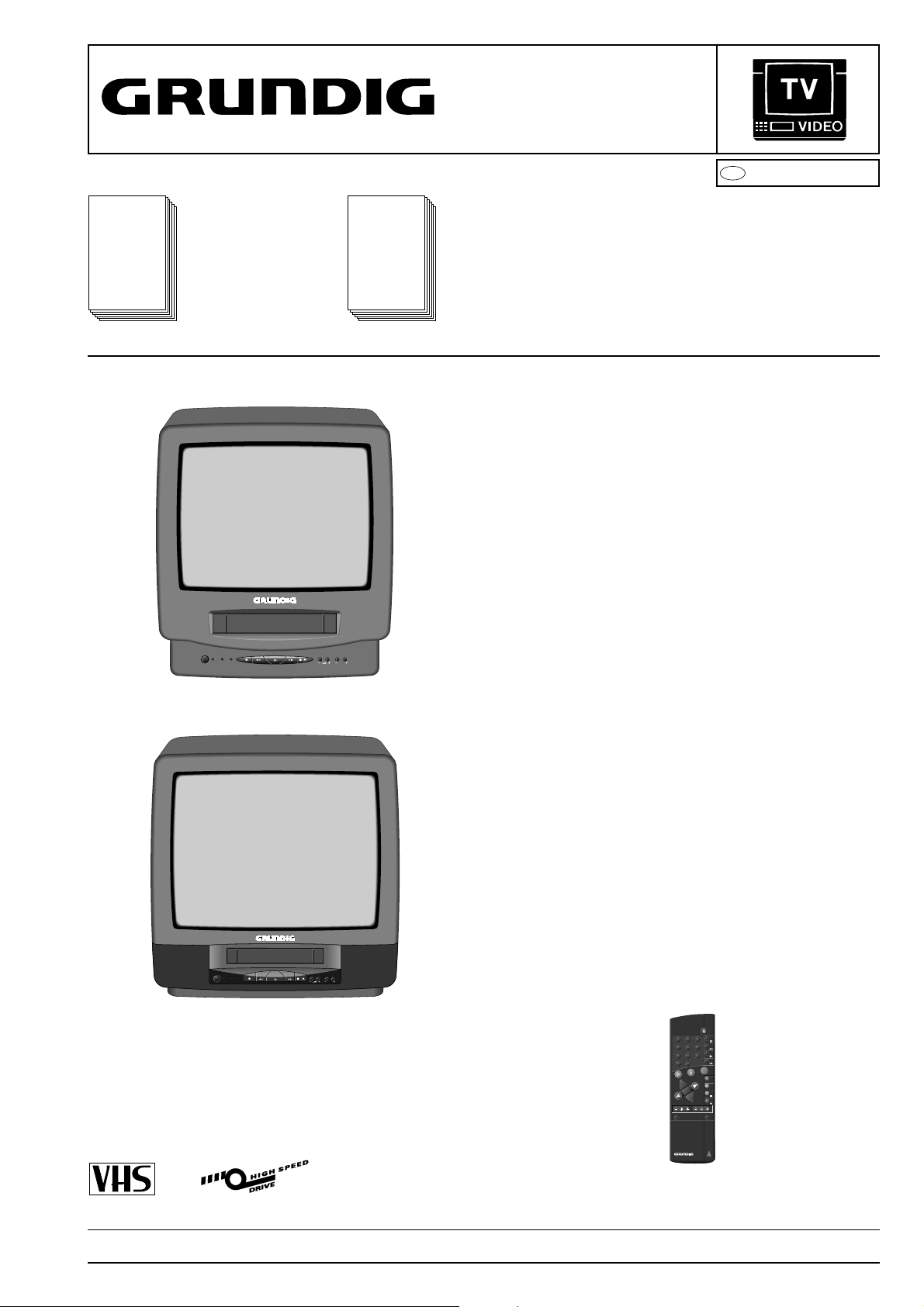
SERVICE MANUAL
D
Btx * 32700
#
Service
Manual
TVR 3710 …
TVR 5100 …
TVR 5500 …
Sach-Nr./Part No.
72010-524.95
Zusätzlich erforderliche Unterlagen
für den
Komplettservice:
Additionally required
Service Manuals for
the Complete Service:
Service
Manual
Sicherheit
Safety
Sach-Nr./Part No.
72010-800.00
TVR 3710 …
TVR 5100 …
TVR 5500 …
TVR 3710 (77250-020.75 / G.CC 2675) TVP 762
TVR 3710 GB (77250-023.75 / G.CC 28-75 GB) TVP 762
8
RECORD
TIMER
P
TVR 5100 (77250-030.75 / G.CC 3075) TVP 762
TVR 5100 (77250-031.75 / G.CC 3175) TVP 762
TVR 5100 (77250-032.75 / G.CC 3275) TVP 762
TVR 5500 (77250-040.75 / G.CC 3475) TVP 762
8
RECORD
TIMER
P
321
4 5 6
7 8 9
P/C
0
AV
CL
TXT
NEXT
+
P
+
PREV.
OK
-
P
OTR
SAT
VIDEO/TV
TVP 762
TVP 762
PAL / SECAM
Änderungen vorbehalten Printed in Germany Service Manual Sach-Nr.
Subject to alteration VK 21/1 0596 Service Manual Part No. 72010-524.95
(77988-017.06)
Page 3

Allgemeiner Teil / General Section TVR 3710 …, TVR 5100 …, TVR 5500 …
Es gelten die Vorschriften und Sicherheitshinweise
gemäß dem Service Manual "Sicherheit", Sach-Nummer 72010-800.00, sowie zusätzlich die eventuell
abweichenden, landesspezifischen Vorschriften!
D
Inhaltsverzeichnis
Seite
Allgemeiner Teil................................... 1-1…1-16
Geräteübersicht ........................................................................... 1-3
Meßgeräte / Meßmittel................................................................. 1-4
Technische Daten ........................................................................ 1-4
Bedienhinweise ............................................................................ 1-5
Servicehinweise ........................................................................... 1-9
Servicetestprogramm................................................................. 1-12
Beschreibung.......................................... 2-1…2-8
Leistungs-Chassis (PLSP) ........................................................... 2-1
• Netzteil ...................................................................................... 2-1
• Hochspannungsteil ................................................................... 2-2
Bildrohrplatte................................................................................ 2-2
Signal-Chassis (PSSP2) .............................................................. 2-3
• Laufwerksteuerung / Deck-Elektronik (DE) ............................... 2-3
• Bedieneinheit (CO) ................................................................... 2-4
• TV-Signalelektronik (TV) ........................................................... 2-4
• Empfangseinheit 2 (TU2) .......................................................... 2-5
• IN/OUT (IO)............................................................................... 2-6
• Video/Chroma (VS) ................................................................... 2-6
• Standardton (AL)....................................................................... 2-7
• Teletext "DOS" (TXT)................................................................ 2-8
Abgleich .................................................. 3-1…3-4
Abgleichlageplan.......................................................................... 3-1
Leistungs-Chassis (PLSP) ........................................................... 3-3
Bildrohrplatte................................................................................ 3-3
Signal-Chassis (PSSP2) .............................................................. 3-3
• TV-Signalelektronik (TV) ........................................................... 3-3
• Bedieneinheit (CO) ................................................................... 3-3
• Laufwerksteuerung / Deck-Elektronik (DE) ............................... 3-4
• Empfangseinheit 2 (TU2) .......................................................... 3-4
• Video/Chroma (VS) ................................................................... 3-4
• Standardton (AL)....................................................................... 3-4
Platinenabbildungen
und Schaltpläne ................................... 4-1…4-72
Verdrahtungspläne....................................................................... 4-1
Blockschaltpläne .......................................................................... 4-7
Netzschalterplatte ...................................................................... 4-18
Leistungs-Chassis (PLSP) ......................................................... 4-19
Bildrohrplatte.............................................................................. 4-33
Laufwerkplatte – Sensoreneinheit.............................................. 4-46
Signal-Chassis (PSSP2) ............................................................ 4-37
• Bedieneinheit (CO) ................................................................. 4-43
• Laufwerksteuerung / Deck-Elektronik (DE) ............................. 4-49
• TV-Signalelektronik (TV) ......................................................... 4-51
• Empfangseinheit 2 (TU2) ........................................................ 4-55
• Teletext "DOS" (TXT).............................................................. 4-58
• IN/OUT (IO)............................................................................. 4-59
• Video/Chroma (VS) ................................................................. 4-61
• Standardton (AL)..................................................................... 4-65
Buchsenplatte (BUPI) ................................................................ 4-68
Kopfverstärkerplatte (OHA)........................................................ 4-69
• Kopfscheibenmotoransteuerung ............................................. 4-70
• Kopfverstärker......................................................................... 4-71
Laufwerk .............................................. 5-1…5-12
Meßgeräte / Meßmittel................................................................. 5-1
Servicehinweise ........................................................................... 5-2
Auswechseln von Laufwerksteilen ............................................... 5-3
Einstellungen ............................................................................. 5-10
Explosionszeichnungen
und Ersatzteillisten............................. E-1…E-11
The regulations and safety instructions shall be valid
as provided by the "Safety" Service Manual, part
number 72010-800.00, as well as the respective
national deviations.
GB
Table of Contents
Page
General Section.................................... 1-1…1-16
TVR Overview .............................................................................. 1-3
Test Equipment / Jigs .................................................................. 1-4
Specifications............................................................................... 1-4
Operating Hints ............................................................................ 1-7
Service Instructions...................................................................... 1-9
Service Test Programme ........................................................... 1-12
Description ........................................... 2-9…2-16
Power Chassis (PLSP) ................................................................ 2-9
• Power Supply ............................................................................ 2-9
• High Voltage Section .............................................................. 2-10
Tube PCB .................................................................................. 2-10
Signal Chassis (PSSP2) ............................................................ 2-11
• Deck Control / Deck Electronic (DE) ....................................... 2-11
• Keyboard Control Unit (CO) .................................................... 2-12
• TV Signal Electronics (TV) ...................................................... 2-12
• Frontend 2 (TU2) .................................................................... 2-13
• IN/OUT (IO)............................................................................. 2-14
• Video/Chroma (VS) ................................................................. 2-14
• Standard Sound (AL) .............................................................. 2-15
• Teletext "DOS" (TXT).............................................................. 2-16
Adjustment Procedures......................... 3-1…3-6
Location of Adjustment Controls .................................................. 3-1
Power Chassis (PLSP) ................................................................ 3-5
Tube PCB .................................................................................... 3-5
Signal Chassis (PSSP2) .............................................................. 3-5
• TV Signal Electronics (TV) ........................................................ 3-5
• Keyboard Control Unit (CO) ...................................................... 3-5
• Deck Control / Deck Electronic (DE) ......................................... 3-6
• Frontend 2 (TU2) ...................................................................... 3-6
• Video/Chroma (VS) ................................................................... 3-6
• Standard Sound (AL) ................................................................ 3-6
Layout of the PCBs
and Circuit Diagrams.......................... 4-1…4-72
Wiring Diagrams .......................................................................... 4-1
Block Circuit Diagrams................................................................. 4-7
Power Switch Board................................................................... 4-18
Power Chassis (PLSP) .............................................................. 4-19
Tube PCB .................................................................................. 4-33
Tape Deck Sensor Panel ........................................................... 4-46
Signal Chassis (PSSP2) ............................................................ 4-37
• Keyboard Control Unit (CO) .................................................... 4-43
• Deck Control / Deck Electronic (DE) ....................................... 4-49
• TV Signal Electronics (TV) ...................................................... 4-51
• Frontend 2 (TU2) .................................................................... 4-55
• Teletext "DOS" (TXT).............................................................. 4-58
• IN/OUT (IO)............................................................................. 4-59
• Video/Chroma (VS) ................................................................. 4-61
• Standard Sound (AL) .............................................................. 4-65
Socket Board (BUPI).................................................................. 4-68
Head Amplifier Board (OHA)...................................................... 4-69
• Headwheel Motor Control ....................................................... 4-70
• Head Amplifier ........................................................................ 4-71
Drive Mechanism................................. 5-1…5-12
Test Equipment / Jigs .................................................................. 5-1
Service Instructions...................................................................... 5-2
Replacement of Tape Deck Components .................................... 5-3
Adjustments ............................................................................... 5-10
Exploded Views and
Spare Parts Lists................................. E-1…E-11
1 - 2 GRUNDIG Service
Page 4
TVR 3710 …, TVR 5100 …, TVR 5500 … Allgemeiner Teil / General Section
Allgemeiner Teil / General Section
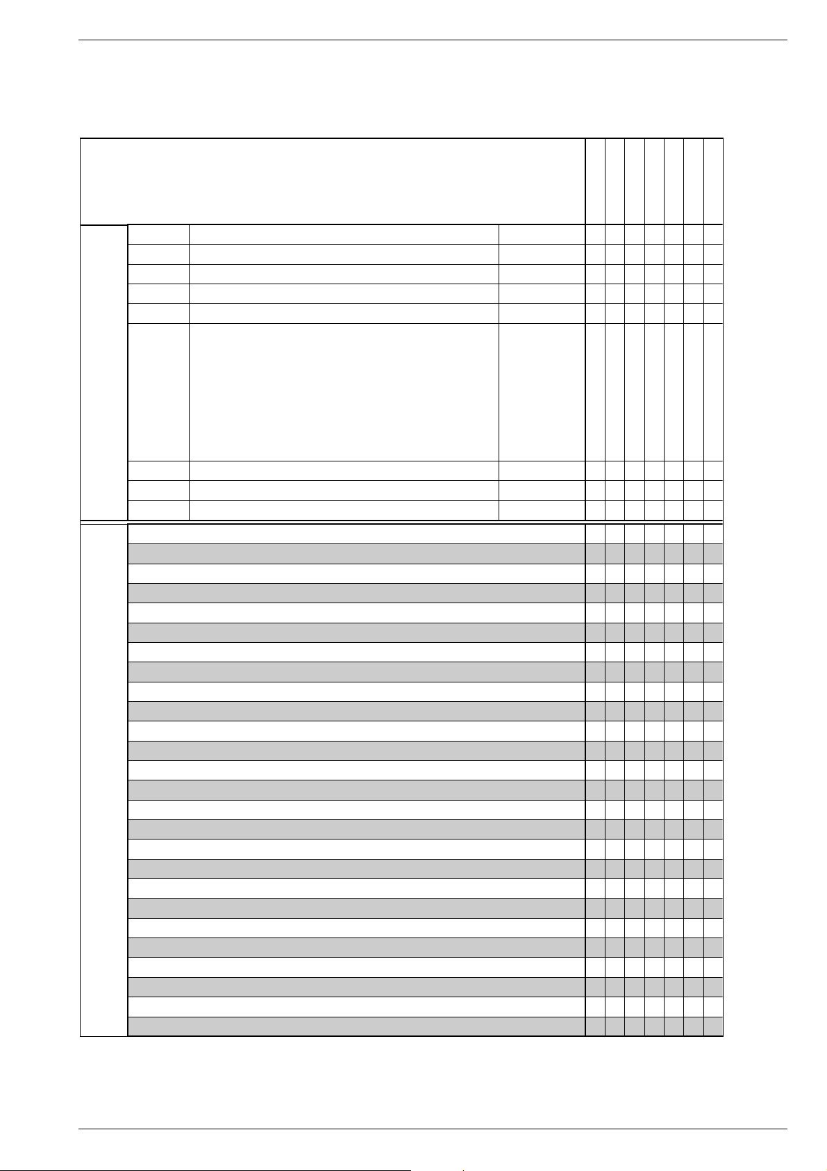
Geräteübersicht / TVR Overview
TVR 3710
TVR 3710 FR
TVR 3710 GB
TVR 5100
TVR 5100 FR
TVR 5500
TVR 5500 FR
S./P 4-19 Leistungs-Chassis / Power PCB (PLSP) —
S./P 4-33 Bildrohrplatte / Tube PCB —
S./P 4-33 Netzschalterplatte / Power Switch Board —
S./P 4-46 Laufwerkplatte-Sensoreneinheit / Tape Deck Sensor Panel 75988-025.06
S./P 4-46 Laufwerkplatte-Sensoreneinheit / Tape Deck Sensor Panel 75988-018.22
S./P 4-37
S./P 4-43
S./P 4-49
S./P 4-51
S./P 4-55
S./P 4-58
S./P 4-59
Table of Moduls
S./P 4-61
S./P 4-65
Geräte-Bausteinübersicht
S./P 4-68 Buchsenplatte / Socket Board (BUPI) —
S./P 4-69 Kopfverstärker / Head Amplifier (OHA) 27599-004.07
S./P 4-69 Kopfverstärker / Head Amplifier (OHA) 27599-004.08
CCIR, B/G/H - PAL
CCIR, I - PAL
CCIR, B/G/L/L' - SECAM
NTSC-Wiedergabe / NTSC Playback
2 Empfangseinheiten / Frontend (Tuner)
Bildschirmdiagonale 37cm (sichtbares Bild: 34cm) / Screen diagonale 37cm (visible picture: 34cm)
Bildschirmdiagonale 51cm (sichtbares Bild: 48cm) / Screen diagonale 51cm (visible picture: 48cm)
Bildschirmdiagonale 55cm (sichtbares Bild: 51cm) / Screen diagonale 55cm (visible picture: 51cm)
Ablenkwinkel / Deflection angle 90
High Speed Drive (HSD)
2-Kopf/Head
Normalplay
Longplay
VISS
ATS euro plus
"On Screen Display" (OSD)
Table of Features
VPS
Geräte-Feature-Übersicht
PDC
Teletext "DOS"
SHOW VIEW
VIDEO Plus
6 Timer
69 Programme + 1 AV
Kopfhörerbuchse / Headphone Jack
EURO-AV-Buchse / Socket
LINE/CV-Buchsen / Sockets
1) nur für Version / only for version G.CC 31-75 / G.CC 32-75
Signal-Chassis (PSSP2)
• Bedieneinheit / Keyboard Control Unit (CO)
• Laufwerksteuerung / Deck Control/Deck Electronic (DE)
• TV-Signalelektronik / TV Signal Electronics (TV)
• Empfangseinheit 2 (TU2)
• Teletext (TXT)
• IN/OUT (IO)
• Video/Chroma (VS)
• Standardton / Standard Sound (AL)
—
• • • • • • •
• • • • • • •
• • • •
• • • •
• • •
• • • • • • •
• • • • • • •
• • • • • •
•
• • • • • •
• • • •
• • •
• • • • • • •
• • •
• • •
• •
• •
• • • • • • •
• • • •
• • • • • • •
• • • • • • •
•
• • • • • • •
• • • • • • •
• • • • • • •
• • • •
• • •
1)
• • • • • •
• • • • • •
•
• • • • • • •
• • • • • • •
• • • • • • •
• • • • • • •
• • • • •
•
GRUNDIG Service 1 - 3
Page 5

Allgemeiner Teil / General Section TVR 3710 …, TVR 5100 …, TVR 5500 …
Meßgeräte / Meßmittel
Regeltrenntrafo Farbgenerator
Zweikanaloszilloskop Tongenerator
Digitalmultimeter Stabilisiertes Netzgerät
Millivoltmeter Frequenzzähler
Beachten Sie bitte das Grundig Meßtechnik-Programm, das Sie unter
folgender Adresse erhalten:
Grundig electronics GmbH
Würzburger Str. 150
D-90766 Fürth/Bay.
Tel. 0911/703-0
Telefax 0911/703-4479
Sach-Nr.
Testcassette..................................................................9.27540-1011
Testcassette (HiFi)........................................................9.27540-1016
Drehmomentmesser 600gf-cm .....................................75987-262.72
Adapter für Drehmomentmesser 600gf-cm...................75987-262.73
Einstellschraubendreher ............................................... 75987-262.80
Bandzug-Einstellgriff und -stift ...................................... 75988-002.27
Kopfscheibenabzieher ..................................................75988-002.37
Nylonhandschuhe ......................................................... handelsüblich
Tentelometer................................................................. handelsüblich
Diese Meßmittel können Sie über die Serviceorganisation beziehen.
Wir weisen jedoch darauf hin, daß es sich hierbei z.T. um Meßmittel
handelt, die am Markt bereits eingeführt sind.
Testcassette Sach-Nr. 9.27540-1011
• Farbtestbild mit Dropout-Einblendung
• 6,3kHz-Senkrecht-Vollspuraufzeichnung und Bezugspegel 333Hz
in dreiminütigem Wechsel.
Testcassette (HiFi) Sach-Nr. 9.27540-1016
• Farbtestbild mit Dropout-Einblendung
• Längsspur-Ton: 6,3kHz und 333Hz
• FM-Ton: 1kHz Vollpegel (± 50kHz Hub)
Video-Lehrfilm Sach-Nr. 72007-744.81
• Laufwerk "High Speed Drive"
Test Equipment / Jigs
Variable isolating transformer Colour generator
Dual channel oscilloscope AF Generator
Digital multimeter Stabilized power supply
Millivoltmeter Frequency counter
Please note the Grundig Catalog "Test and Measuring Equipment"
obtainable from:
Grundig electronics GmbH
Würzburger Str. 150
D-90766 Fürth/Bay.
Tel. 0911/703-0
Telefax 0911/703-4479
Part no.
Test cassette.................................................................9.27540-1011
Test cassette (HiFi)....................................................... 9.27540-1016
Torquemeter 600gf-cm .................................................75987-262.72
Adapter for Torquemeter 600gf-cm...............................75987-262.73
Adjustment screw driver................................................75987-262.80
Tape tension adjustment tool - handle and - pin........... 75988-002.27
Headwheel extractor .....................................................75988-002.37
Nylon gloves ....................................................... commonly available
Tentelometer....................................................... commonly available
You can order these test equipments from the Service organization. We
refer to you that these test equipments are already obtainable on the
market.
Test cassette Part no. 9.27540-1011
• Colour test pattern with dropout recording
• 6.3kHz vertical full-track recording alternating with 333Hz reference
level every 3 minutes.
Test cassette (HiFi) Part no. 9.27540-1016
• Colour test pattern with dropout recording
• Longitudinal track sound: 6.3kHz and 333Hz
• FM sound: 1kHz full level (± 50kHz deviation)
Video Training Film Part no. 72007-744.81
• Drive mechanism "High Speed Drive"
Technische Daten
Bildröhre
Sichtbares Bild ................................. siehe Geräte-Feature-Übersicht
Bildschirmdiagonale ......................... siehe Geräte-Feature-Übersicht
Ablenkwinkel ................................................................................. 90°
Bildwechselfrequenz .................................................................. 50Hz
FS-Norm.......................................... siehe Geräte-Feature-Übersicht
CCIR, B/G/H - PAL
CCIR, I - PAL
CCIR, B/G/L/L´- SECAM
VHS-System
1/2” Video - Cassettenrecorder
Bandgeschwindigkeit ......................................................... 2,339cm/s
Aufzeichnungsgeschwindigkeit .............................................. 4,84m/s
Video
Auflösung (VHS) .................................................................. ca. 3MHz
Ton
Frequenzgang:................................................... 80Hz…10kHz ≤ 8dB
Musikleistung: ............................................................................... 4W
Netzspannung ................................................................. 195…264V
Netzfrequenz ....................................................................... 50/60Hz
Leistungsaufnahme
– TV-Betrieb ......................................................... ≤ 70W (TVR 3710…)
≤ 80W (TVR 5100…)
≤ 95W (TVR 5500…)
– Aufnahme............................................................................ca. 25W
– Stand by................................................................................ ≤ 10W
Umgebungstemperatur ............................................ +10°C…+35°C
Relative Luftfeuchte................................................................≤ 80%
Betriebslage ...................................................................... horizontal
Specifications
Picture Tube
Visible picture................................................... see Table of Features
Screen diagonale ............................................. see Table of Features
Deflection angle ............................................................................ 90°
Vertical frequency ...................................................................... 50Hz
VTV standard ..................................................see Table of Features
CCIR, B/G/H - PAL
CCIR, I - PAL
CCIR, B/G/L/L´- SECAM
VHS-System
1/2” video cassette recorder
Tape speed ........................................................................ 2.339cm/s
Head to tape speed................................................................ 4.84m/s
Video
Video resolution (VHS) ................................................ approx. 3MHz
Sound
Frequency response: ......................................... 80Hz…10kHz ≤ 8dB
Music power:................................................................................. 4W
Mains voltage .................................................................. 195…264V
Mains frequency.................................................................. 50/60Hz
Power consumption
– TV mode ........................................................... ≤ 70W (TVR 3710…)
≤ 80W (TVR 5100…)
≤ 95W (TVR 5500…)
– Record ........................................................................ approx. 25W
– Stand by mode...................................................................... ≤ 10W
Ambient temperature ................................................ +10°C…+35°C
Relative humidity .................................................................... ≤ 80%
Operating position ............................................................ horizontal
1 - 4 GRUNDIG Service
Page 6
❒
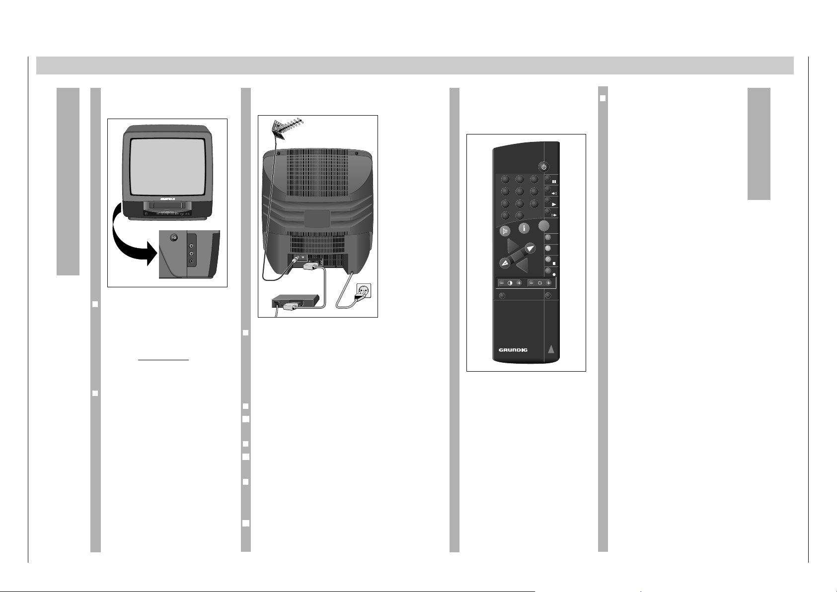
Die Tasten der Fernbedienung
0
...
9
AV Ziffern-Tasten für verschiedene Ein-
gaben.
m
CL Zum manuellen Einstellen der
Sender;
löscht Eingaben.
¢
+
Schaltet den Ton ab.
.
Zum Abrufen von Informationen auf
den Bildschirm.
|]
Wählt den Programmplatz (bei
Stopp);
zum Anwählen verschiedener Funktionen in den Info-Tafeln.
xc
Zum Verändern der Lautstärke;
Wählt Daten in den Info-Tafeln.
G Bestätigt Daten.
™ Verändert den Farbkontrast.
® Verändert die Helligkeit.
¢VIDEO/TV Schaltet die Fernbedienung um zur
Bedienung eines GRUNDIG Videorecorders oder Fernseh es.
¢SAT Schaltet die Fernbedienung um zur
Bedienung eines GRUNDIG Satellitenempfängers.
¢
•
OTR Startet die Aufnahme.
¢
■
Beendet alle Funktionen (Stopp)
außer Timer-Aufnahme.
¢PREV. Sucht den Beginn der aktuellen Auf-
zeichnung.
¢NEXT Sucht den Beginn der nächsten Auf-
zeichnung.
¢
TXT
Schaltet auf Videotext-Betrieb.
¢
de Bildsuchlauf vorwärts bei
Wiedergabe;
Vorlauf bei Stopp.
¢
e Startet die Wiedergabe.
¢
rf Bildsuchlauf rückwärts bei
Wiedergabe;
Rücklauf bei Stopp.
¢
II Pause bei Aufnahme;
Standbild bei Wiedergabe.
b
Schaltet den TVR in Bereitschaft
(Stand-by).
Bedienhinweise Hinweis: Dieses Kapitel enthält Auszüge aus der Bedienungsanleitung. Weitergehende Informationen entnehmen Sie bitte der gerätespezifischen Bedienungsanleitung, deren Sachnummer Sie in der entsprechenden Ersatzteilliste finden.
TVR 3710 …, TVR 5100 …, TVR 5500 … Allgemeiner Teil / General Section
GRUNDIG Service 1 - 5
Auf einem Blick
Auf dieser Seite sind die Tasten der Fernbedienung
kurz erklärt. Die Bedienung entnehmen Sie bitte
dem jeweiligen Kapitel dieser Bedienungsanleitung.
Die Fernbedienung
❒
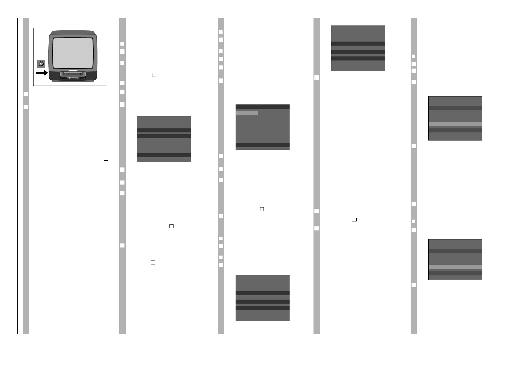
Buchsen
–II–
Antennenbuchse
EURO AV EURO AV Buchse zum Anschluß eines
Satellitenreceivers, Videorecorders,
PAY-TV-Decoder usw.
Anschließen
❒
TVR an das Stromnetz anschließen
Stecken Sie den Stecker des Netzkabels in die
Steckdose.
❒
TVR an die Antenne anschließen
Stecken Sie den Stecker des Antennenkabels in die
Antennenbuchse –II–des TVR's.
❒
"Pay-TV"-Decoder anschließen
Wenn Sie verschlüsselte Fernseh-Programme
privater Anbieter empfangen und aufzeichnen wollen, ist ein Decoder notwendig. Fragen Sie im Fachhandel.
Verbinden Sie den Decoder über ein EURO-AVKabel mit der Buchse EURO-AV des TVR's.
1
1
1
RückseiteVorderseite
❒
Bedienelemente und Buchsen an der Seite
ü Netztaste
U Kopfhörerbuchse 3,5 mm ø.
Der eingebaute Lautsprecher wird
beim Einstecken des Kopfhörers automatisch abgeschaltet.
Unter der Abdeckung:
AUDIO Toneingangsbuchsen
VIDEO Bildeingangsbuchse
❒
Bedienelemente an der Vorderseite
A Beendet alle Funktionen (außer
Timer);
Schaltet den TVR ab (Stand-by).
L Startet die Aufnahme.
o Bildsuchlauf rückwärts bei Wieder-
gabe;
Band zurückspulen bei Stopp.
R Startet die Wiedergabe.
p Bildsuchlauf vorwärts bei Wieder-
gabe;
Band vorspulen bei Stopp.
r Beendet alle Funktionen (Stopp).
Schiebt die Cassette aus.
¢
–V + Lautstärke
¢
– P + Programmwahl
Bedienelemente und Anschließen
PAY-TV
VIDEO/TV
SAT
OK
P
+
P
-
AV
321
4 5 6
7 8 9
P/C
0
NEXT
+
PREV.
TXT
OTR
CL
TVP 762
8
RECORD
TIMER
P
AUDIO
VIDEO
U
EURO AV
Page 7
Einstellungen
Fernseh-Programme einstellen,
mit dem Suchlauf-Speicher-System
(ATS euro plus)
❒
Vorbereiten
TVR einschalten.
❒
Bedienung
w
!
Beim erstmaligen Betrieb setzen Sie die Einstellung
bitte mit Punkt fort.
GRUNDIG-INFOCENTER mit Taste h aufrufen.
»INSTALLATION« mit den Tasten
| ]
anwählen
und mit Taste G aufrufen.
»ATS EURO PLUS« wählen und mit Taste G
aktivieren.
Die Tafel »SPRACHE« erscheint.
Sprache der Benutzerführung mit den Tasten
| ]
wählen und mit Taste G bestätigen.
Land (Aufstellungsort) mit den Tasten
| ]
wählen.
ATS euro plus-Suchlauf mit Taste G starten.
– Anzeige am Bildschirm: »ATS-SUCHT«.
Der TVR sucht alle Kanalzahlen nach FernsehProgrammen ab, sortiert und speichert sie.
– Nach Abschluß des Suchlaufs erscheint die Tafel
»INSTALLATION«.
w
!
Wie Sie die Reihenfolge der Fernseh-Programme
ändern, lesen Sie ab Punkt im Kapitel »Fernsehprogramme umsortieren« auf der nächsten Seite,
oder
Einstellung mit Taste h beenden.
w
!
Wird ein Neulauf erforderlich (z.B. Wohnortwechsel, Kabelanschluß), wiederholen Sie die Einstellung ab Punkt .
1
7
4
6
5
4
SPRACHE
D
I
E
P
M N OK
3
2
1
4
1
TVR ein/ausschalten
Netzschalter an der linken Gerätseite drücken.
Die rote Anzeige leuchtet.
Einschalten aus Stand-by:
Mit den Zifferntasten 0… 9,
oder der Taste ]der Fernbedienung,
oder der Taste ¢P+ am Gerät,
oder durch Einschieben einer Cassette,
oder durch Starten der Wiedergabe (wenn eine
Cassette im TVR ist).
Mit Taste bschalten Sie den TVR aus (Stand-by).
w
!
Beim erstmaligen Betrieb erscheint die Tafel
»SPRACHE«. Führen Sie die folgenden Einstellungen im Kapitel »Fernsehprogramme einstellen mit
dem Suchlauf-Speicher-System« ab Punkt
durch.
Fernseh-Programme einstellen
Die Fernsehanstalten senden ihre Programme
durch Fernsehsender auf verschiedenen Frequenzen/Kanälen.
Vorher müssen Sie die Kanäle der FernsehProgramme am TVR einstellen.
Es stehen 69 Programmplätze zur Verfügung, die
beliebig mit Fernseh-Programmen von der Antenne
oder dem Kabelanschluß belegt werden können.
Zum Einstellen gibt es zwei Möglichkeiten:
1. Mit dem Suchlauf-Speicher-System (ATS euro
plus). Der TVR sucht, sortiert und speichert alle
Kanalzahlen/Sonderkanalzahlen, die er an seinem
Standort empfangen kann.
Dieser Vorgang ist abhängig von der von Ihnen
gewählten Sprache, dem gewählten Land und der
Empfangsqualität der Fernseh-Programme.
Sollte Ihnen die vorgegebene Reihenfolge der
Fernseh-Programme nicht zusagen, können Sie
dies nachträglich ändern.
2. Durch direkte Eingabe der Daten.
4
2
1
Allgemeiner Teil / General Section TVR 3710 …, TVR 5100 …, TVR 5500 …
1 - 6 GRUNDIG Service
Fernseh-Programme umsortieren
❒
Vorbereiten
TVR mit Netztaste einschalten.
❒
Bedienung
GRUNDIG-INFOCENTER mit Taste h aufrufen.
»INSTALLATION« mit den Tasten
| ]
anwählen
und mit Taste G aufrufen.
»SORTIERUNG PROG. NR.« mit den Tasten
| ]
anwählen und mit Taste G aufrufen.
– Eine Tafel mit Angabe des Programmplatzes und
des Kanals oder der Frequenz erscheint.
Der gewählte Programmplatz ist markiert.
Programmplatz mit den Tasten
| ]
anwählen
und mit Taste G markieren.
Neuen Programmplatz mit den Tasten
| ]
anwählen.
Einstellungen mit Taste G speichern.
– Die Daten des markierten Programmplatzes wer-
den an den neuen Programmplatz verschoben.
– Die folgenden Fernseh-Programme verschieben
sich um eine Position.
w
!
Zum Umsortieren von weiteren Fernseh-Programmen Vorgang ab Pkt. wiederholen.
Einstellung mit Taste h beenden.
Daten von Hand eingeben
❒
Vorbereiten
TVR einschalten.
❒
Bedienung
Taste
m
CL drücken.
– Die Tafel »MAN. ABSTIMMUNG« erscheint.
MAN. ABSTIMMUNG
PR C/F CH DEC FA
01 C 06 ON 00
M N T Z OK
1
1
7
4
6
5
4
SORTIERUNGPROG. NR.
01 C06
02 C34
03 C59
04 C40
05 C36
06 C21
M N OK
3
2
1
1
Option
Position mit den Tasten E F wählen.
Die Texte bedeuten:
PR: Programmplatz
C/F, FREQU: C (=Kanal) oder F (=Frequenz) des
Fernseh-Programms,
CH: Kanal
SY: Norm (PAL BG, SECAM L, PAL I)
F: Frequenz
DEC: Programmplatz für externen
Decoder aktivieren,
FA, SF: Bild feinabstimmen.
w
!
Die weitere Bedienung entnehmen Sie bitte den
Dialogzeilen der Tafel.
w
!
Alternativ zur Eingabe der Kanalzahl kann die Sonderkanalzahl oder die Frequenz des Fernseh-Programms eingegeben werden, dazu mit Tasten
E F »C/F« anwählen und mit den Tasten
| ]
gewünschte Einstellung wählen.
– »C« = Kanaleingabe
»S« = Sonderkanal
»F« = Frequenzeingabe.
Gewünschten Kanal/Sonderkanal zweistellig, oder
gewünschte Frequenz dreistellig mit den ZiffernTasten 0 … 9 eingeben.
w
!
Sind Kanalzahl oder Frequenz nicht bekannt, kann
der Suchlauf gestartet werden, dazu Taste ] oder
|
drücken.
Eingabe mit Taste G speichern.
Zur Dateneingabe für die nächsten Programmplätze
Einstellung ab Pkt. wiederholen.
Einstellung mit Taste h beenden.
4
2
3
2
SYNT. MANUELLE
PR F FREQU SY DEC SF
01 F 285 L ON 00
M N T Z OK
Die Kindersicherung
Mit der Kindersicherung lassen sich alle Funktionen
verriegeln.
Selbst eine Cassette, die nachträglich eingeschoben
wird, muß im TVR bleiben, bis Sie ihn wieder
entriegeln.
❒
Kindersicherung aktivieren
GRUNDIG-INFOCENTER mit Taste h aufrufen.
»SPEZIAL« mit den Tasten
| ]
wählen und mit
Taste G aufrufen.
»KINDERSICHERUNG« mit den Tasten
| ]
anwählen und mit Taste G aufrufen.
– Die Tafel »KINDERSICHERUNG« erscheint.
Geheimnummer mit den Ziffern-Tasten 0 … 9
vierstellig eingeben und mit Taste G bestätigen.
w
!
Wird die Kindersperre während einer Wiedergabe
aktiviert, wird diese bis zum Bandende ausgeführt
und das Band an den Anfang zurückgespult.
Danach schaltet der TVR in Bereitschaft.
w
!
Ist der »ABSCHALTTIMER« aktiviert (siehe Seite
23), schaltet sich der TVR bei Erreichen der
Abschaltzeit ab, und aktiviert die Kindersperre.
w
!
Eine programmierte TIMER-Aufnahme wird auch
bei aktivierter Kindersicherung ausgeführt.
TVR mit Taste babschalten.
w
!
Der TVR ist verriegelt und schaltet ab.
❒
Kindersicherung abschalten
Beliebige Taste drücken.
– Die Tafel »KINDERSICHERUNG« erscheint.
Vierstellige Geheimnummer mit den Ziffern-Tasten
0 … 9 eingeben und mit Taste G bestätigen.
– Der TVR schaltet die Tafel ab, die Sperre ist auf-
gehoben.
w
!
Falls Sie die Geheimnummer vergessen oder verlegt haben, drücken sie die Tasten E F
| ]
nacheinander
.
2
KINDERSICHERUNG
ZUM FREIGEBEN
NUMMER EINGEBEN
– – – –
OK
1
5
4
KINDERSICHERUNG
ZUM SPERREN
NUMMER EINGEBEN
– – – –
0 9 OK
3
2
1
8
RECORD
TIMER
P
Page 8
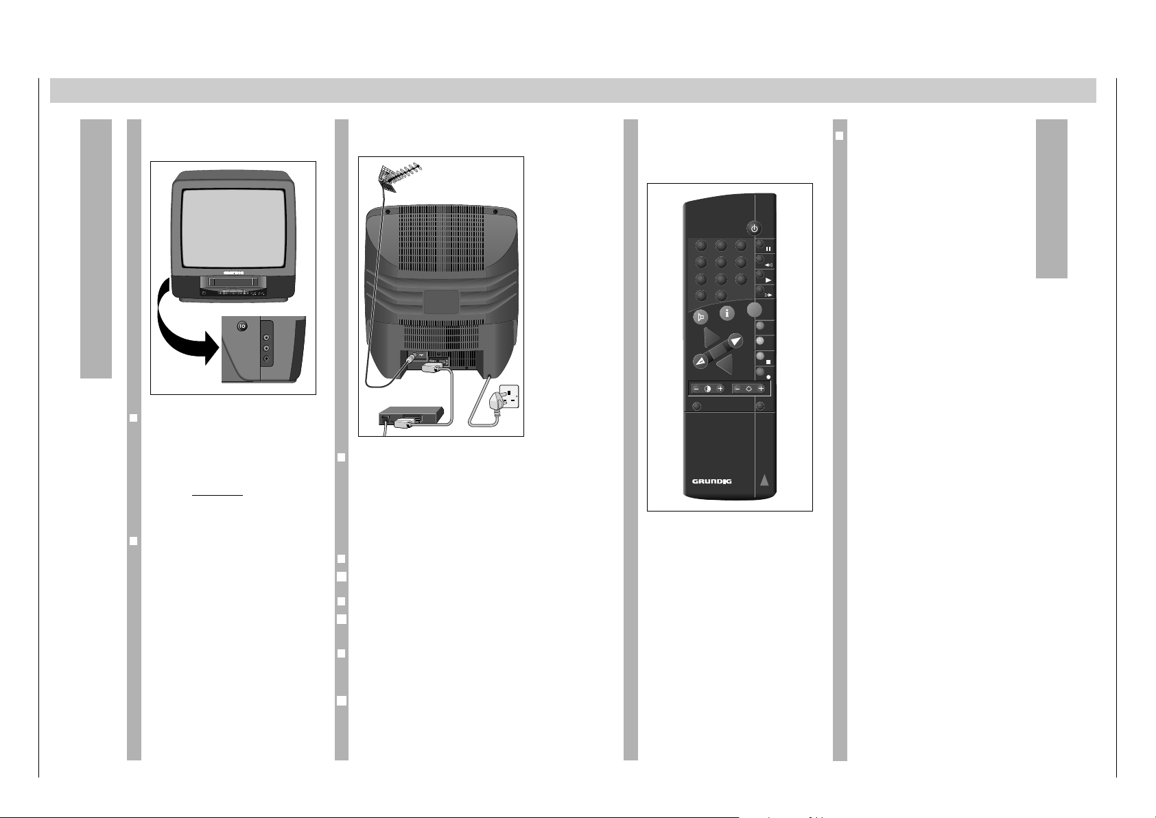
❒
The buttons on the remote control
0
...
9
AV Numbered buttons for various
entries.
m
CL For manually tuning in stations;
clears entries.
¢
+
Switches off the sound.
.
Displays information tables on the
picture screen.
| ]
Selects programme positions (in
Stop position);
selects the various functions in the
info tables.
x c
Alter the volume setting;
select data in the info tables.
G Confirms data.
™ Alters the colour contrast setting.
® Alters the brightness setting.
¢VIDEO/TV Switches the remote control so that
it can be used for a GRUNDIG video
recorder or TV receiver.
¢SAT Switches the remote control so that
it can be used for a GRUNDIG satellite receiver.
¢
•
OTR Starts recording.
¢
■
Ends all functions (stop) except
Timer recordings.
¢PREV. Searches the beginning of the cur-
rent recording.
¢NEXT Searches the beginning of the next
recording.
¢
TXT
Switches to Teletext mode.
¢
de Picture search forwards in playback
mode;
tape fast forward in stop mode.
¢
e Starts playback.
¢
rf Picture search reverse in playback
mode;
rewind tape in stop mode.
¢
II Pause in recording mode,
freeze-frame in playback mode.
b
Switches the TVR to standby.
TVR 3710 …, TVR 5100 …, TVR 5500 … Allgemeiner Teil / General Section
GRUNDIG Service 1 - 7
Operating Hints Note: This chapter contains excerpts from the operating instructions. For further particulars please refer to the appropriate user instructions the part number of which is indicated in the relevant spare parts list.
At a glance
The buttons on the remote control are explained
briefly on this page. For operation, please see the
respective chapter of these operating instructions.
The Remote Control
VIDEO/TV
SAT
OK
P
+
P
-
AV
321
4 5 6
7 8 9
P/C
0
NEXT
+
PREV.
TXT
OTR
CL
TVP 762
❒
Sockets
–II–
Aerial socket
EURO AV EURO AV socket for connecting a
satellite receiver, a video recorder, a
Pay-TV decoder, etc.
Connecting
❒
Connecting the TVR to the mains
Plug the mains cable into the wall socket.
❒
Connecting the TVR to the aerial
Insert the plug of the aerial cable into the TVR aerial
socket –II–.
❒
Connecting a "Pay-TV" decoder
If you want to receive and record scrambled TV
programmes from private TV stations, you need a
decoder. Contact a dealer for more information.
Connect the decoder using a EURO AV cable to the
EURO AV socket of the TVR.
1
1
1
Back of the TVRFront of the TVR
❒
Controls and sockets on the side
ü Power switch
U Headphone socket 3.5 mm ø.
When connecting a headphone, the
built-in loudspeaker is automatically
switched off.
Behind the flap:
AUDIO Audio input sockets.
VIDEO Video input socket.
❒
Controls on the front
A Ends all functions (except the Timer);
switches the TVR to standby.
L Starts recording.
o Picture search reverse in playback
mode;
rewind tape in stop mode.
R Starts playback.
p Picture search forwards in playback
mode;
tape fast forward in stop mode.
r Stops all functions;
ejects the cassette.
¢
–V + Volume
¢
– P + Programme selection
Connecting and Control Elements
EURO AV
PAY-TV
8
RECORD
TIMER
P
AUDIO
VIDEO
U
Page 9
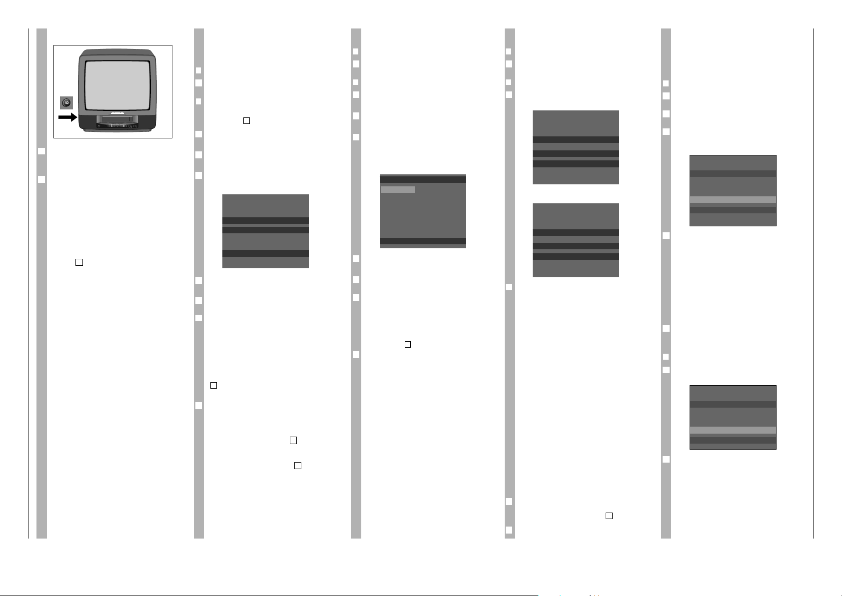
Allgemeiner Teil / General Section TVR 3710 …, TVR 5100 …, TVR 5500 …
1 - 8 GRUNDIG Service
Tuning to TV stations with the
automatic tuning system
(ATS euro plus)
❒
Preparation
Switch the TVR on.
❒
Operation
w
!
When the TVR is operated for the first time, continue with step .
Call up the GRUNDIG-INFOCENTER using the h
button.
Select the "INSTALLATION" line with the
|
or
]
button and confirm with the G button.
Select "ATS EURO PLUS" and confirm with the G
button.
The "LANGUAGE" table appears.
Select the language for your location using the
| ]
buttons and confirm with the G button.
Select the country (location) using the
| ]
buttons.
Start the ATS euro plus search using the G
button.
– Display on TVR: "ATS-SEARCHING".
The TVR searches for TV stations, and sorts and
stores them.
– When the search has been completed, the
"INSTALLATION" table appears.
w
!
How to alter the sequence of TV stations is explained in the chapter "Resorting TV stations" from step
on (see next page).
or
End the setting using the h button.
w
!
If a new run of the ATS should be necessary (for
example, when you have changed your location or
are connnected to a cable system at a later date),
repeat the setting starting at step .
If your TVR is connected to a cable system which
offers the ACI function (Automatic channel Indication), select the "ACI" line after step . ATS then is
started immediately and the TVR takes the channel
numbers from the info table offered by the cable
provider and stores them in memory.
2
1
7
4
6
5
4
LANGUAGE
GB
D
F
M N OK
3
2
1
4
1
Settings
Resorting TV stations
❒
Preparation
Switch on the TVR with the power switch.
❒
Operation
Call up the GRUNDIG-INFOCENTER using the h
button.
Select the "INSTALLATION" line with the
| ]
buttons and confirm with the G button.
"Select RESORT PROG. NR." with the
| ]
buttons and confirm with the G button.
– A table indicating the programme position and the
channel/frequency is displayed. The selected programme position is marked.
Select the programme position with the
| ]
buttons and mark it with the G button.
Select the new programme position with the
| ]
buttons.
Store the setting with the G button.
– The data of the marked programme position will
be transferred to the new programme position.
– The following TV stations are moved by one posi-
tion.
w
!
To sort further TV stations, repeat the procedure
starting at step .
End the setting using the h button.
7
4
6
5
4
RESORT PROG.NR.
01 C06
02 C34
03 C59
04 C40
05 C36
06 C21
M N OK
3
2
1
1
Entering data manually
❒
Preparation
Switch the TVR on.
❒
Operation
Press the
m
CL button.
– The "MANUAL STORE" table appears.
Option
Select the desired item with the E F buttons.
The terms mean:
PR: Programme position.
C/F, FREQU: C (= channel) or F (= frequency) of
the TV programme.
CH: Channel
SY: Norm (PAL BG, SECAM L, PAL I)
F: Frequency
DEC: Activate programme position for
external decoder.
FT, SF: Fine tuning of picture.
w
!
For further operating steps see the dialogue lines of
the table.
w
!
Instead of entering the channel number you can
enter the special channel number or the frequency
of the TV station. To do this, use the E F buttons
to select "C/F" then select the desired item using the
| ]
buttons.
– "C" = Channel entry.
"S" = Special channel entry.
"F" = Frequency entry.
Enter the desired channel/special channel number
as two digits or the frequency as three digits
using the 0 …9 buttons.
w
!
If both the channel number and the frequency are
unknown a search may be started. To do this press
the ] or |button.
Store the entry with the G button.
To enter data for the next programme position,
repeat the setting starting with step .
End the setting with the h button.
4
2
3
2
SYNT. MANUELLE
PR F FREQU SY DEC SF
01 F 285 L ON 00
M N T Z OK
MANUALSTORE
PR C/F CH DEC FT
01 C 06 ON 00
M N T Z OK
1
1
Switching the TVR on and off
Press the power switch located on the left of the
unit.
The red pilot lamp lights up.
The TVR can be switched on from standby:
using the numeric buttons 0… 9,
or the ]button on the remote control,
or the ¢P+ button on the unit,
or by inserting a cassette,
or by starting playback (if a cassette is loaded).
Press the bbutton to switch the TVR to standby.
w
!
When switching the TVR on the first time, the
"LANGUAGE" menu is displayed. Perform the following settings described in the chapter "Tuning to TV
stations with the automatic tuning system" starting
with step .
Tuning to TV stations
Television stations broadcast programmes on different frequencies/channels.
To receive these programmes, you must tune your
TVR to the channels used by the different TV
stations.
69 programme positions are available. They can be
tuned as required to TV stations from the aerial or a
cable connection.
Two options are available for tuning:
1. With the automatic tuning system (ATS euro
plus/ACI). The TVR searches, sorts, and stores
all channels/special channels which can be received at its location.
This procedure depends on the language and
country you select, as well as the quality of
reception of the TV stations.
If you are not satisfied with the order in which
the TV stations are allocated, the order can be
changed later.
2. By entering data directly.
4
2
1
The child lock
It is possible to lock all functions using the child
lock.
Even a cassette which is inserted afterwards
remains in the TVR until it is unlocked.
❒
Activating the child lock
Call up the GRUNDIG-INFOCENTER using the h
button.
Select the "SPEZIAL" option using the
| ]
but-
tons and confirm using the G button.
Select the "CHILD LOCK" option using the
| ]
buttons and confirm using the G button.
– The "CHILD LOCK" table appears.
Enter a four-digit code number using the numbered
buttons 0 … 9 and confirm it using the G
button.
w
!
If the child lock is activated during playback, this is
continued till tape end, then the tape is rewound to
its beginning and the TVR switches to standby.
w
!
If the "SLEEP TIMER" is activated (see page 23), the
TVR switches automatically off when the switch-off
time is reached and activates the child lock.
w
!
A programmed TIMER recording will be executed
even with the child lock activated.
Switch the TVR off using the bbutton.
w
!
The TVR is locked and switched off.
❒
De-activating the child lock
Press any button.
– The "CHILD LOCK" table appears.
Enter the four-digit code number using the numbered buttons 0 … 9 and confirm using the
G button.
– The TVR switches the table off, the lock is de-
activated.
w
!
If you have forgotten or mislaid the personal code,
press the buttons E F
| ]
in this order.
2
CHILD LOCK
ENTER NUMBER
TO UNLOCK
– – – –
OK
1
5
4
CHILD LOCK
ENTER NUMBER
TO LOCK
– – – –
0 9 OK
3
2
1
8
RECORD
TIMER
P
Page 10
TVR 3710 …, TVR 5100 …, TVR 5500 … Allgemeiner Teil / General Section
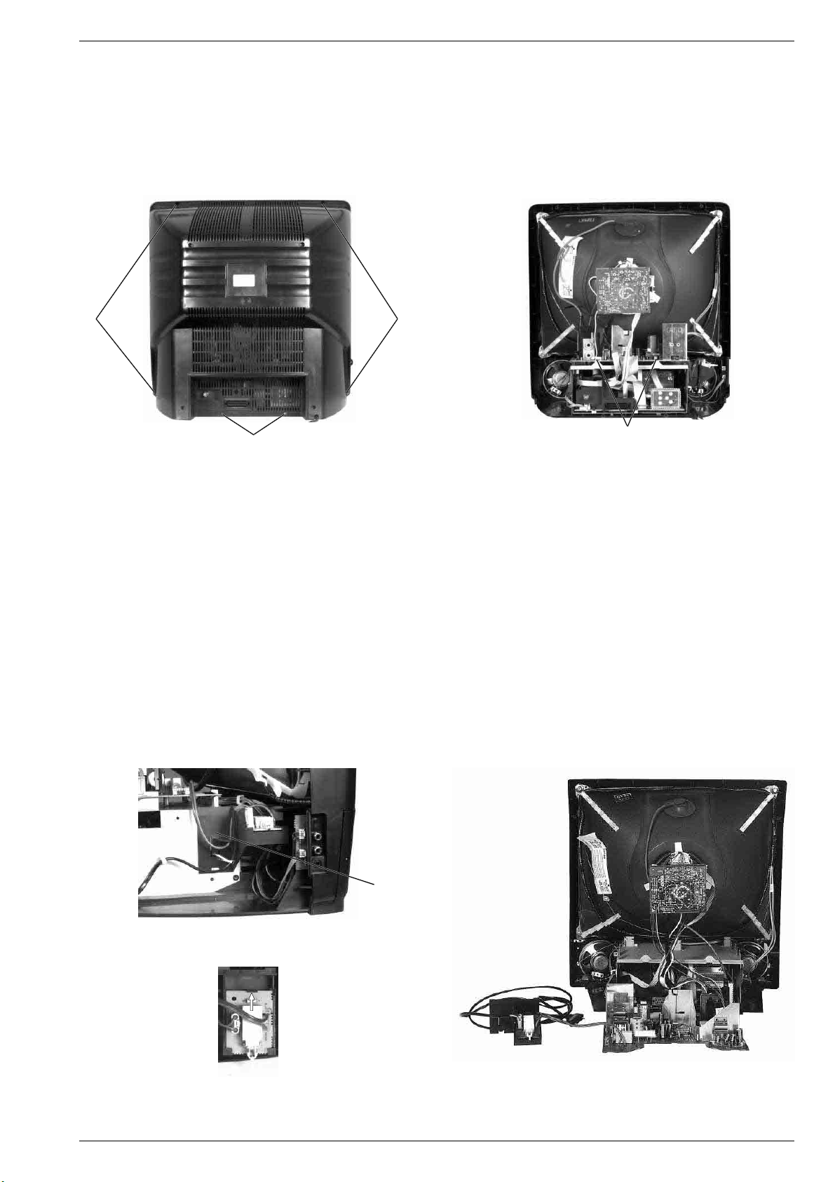
Servicehinweise
1. Ausbauhinweise
1.1 Geräterückwand abnehmen
– Gerät vom Netz trennen.
– 6 Schrauben (Pos. 19) entfernen und Geräterückwand abnehmen
(Fig. 1).
19
19
19
Service Instructions
1. Disassembly Instructions
1.1 Rear Side of the Cabinet
– Disconnect the unit from the mains.
– Undo 6 screws (Pos. 19) and remove the rear side of the cabinet
(Fig. 1).
12
Fig. 2Fig. 1
1.2 Leistungs-Chassis (PLSP) ausbauen
– 2 Schrauben (Pos. 12) entfernen (Fig. 2).
– Steckverbindungen (1921, 1922, 1923, 1924 und 1925) zum Video-
teil und zur Bildröhre lösen (Fig. 6).
– Bei Geräten mit zusätzlicher Netzschalterplatte:
Rastnase (Fig. 3) lösen und Netzschalterplatte mit Halter (Pos. 4)
abmontieren und Netzkabel freilegen.
Achtung: Nur bei einem Defekt auf der Netzschalterplatte die
Rastnase lösen (Fig. 4) und Netzschalterplatte aus dem Halter
nehmen.
– Leistungs-Chassis nach hinten ziehen und nach oben abnehmen.
Achtung: Beim Einbau des Leistungs-Chassis müssen die Ab-
standshalter (Pos. 42, Explosionszeichnung) angebracht
sein.
Betrieb des Gerätes mit ausgebautem Leistungs-Chassis
– Leistungs-Chassis hinter das Gerät wie in Fig. 5 gezeigt legen.
– Steckverbindungen wieder kontaktieren.
Achtung: Das Leistungs-Chassis und die Netzschalterplatte dürfen
dabei nicht das Abschirmgehäuse berühren.
4
1.2 Removing the Power Chassis (PLSP)
– Undo the 2 screws (Pos. 12, Fig. 2)
– Unplug the connectors (1921, 1922, 1923, 1924 and 1925) to the
Video Unit and the picture tube (Fig. 6).
– Concerning TVR's with additional power supply panel:
Disengage the locking lug (Fig. 3), detach the mains switch panel
and the holder (Fig. 4) and uncover the power supply cable.
Attention: Detach the locking lug (Fig. 4) and take out the mains
switch panel from the holder only if the mains switch panel is
defective.
– Withdraw the Power Chassis and take it out towards the top.
Attention: When re-assembling the Power Chassis the spacers must
be fitted (pos. 42, exploded view).
Operating the TVR with the Power Chassis removed
– Place the Power Chassis behind the set as shown in Fig. 5.
– Re-connect the connectors.
Attention: The Power Chassis and the mains switch panel must not
come into contact with the metal screen.
Fig. 3
Fig. 5Fig. 4
GRUNDIG Service 1 - 9
Page 11
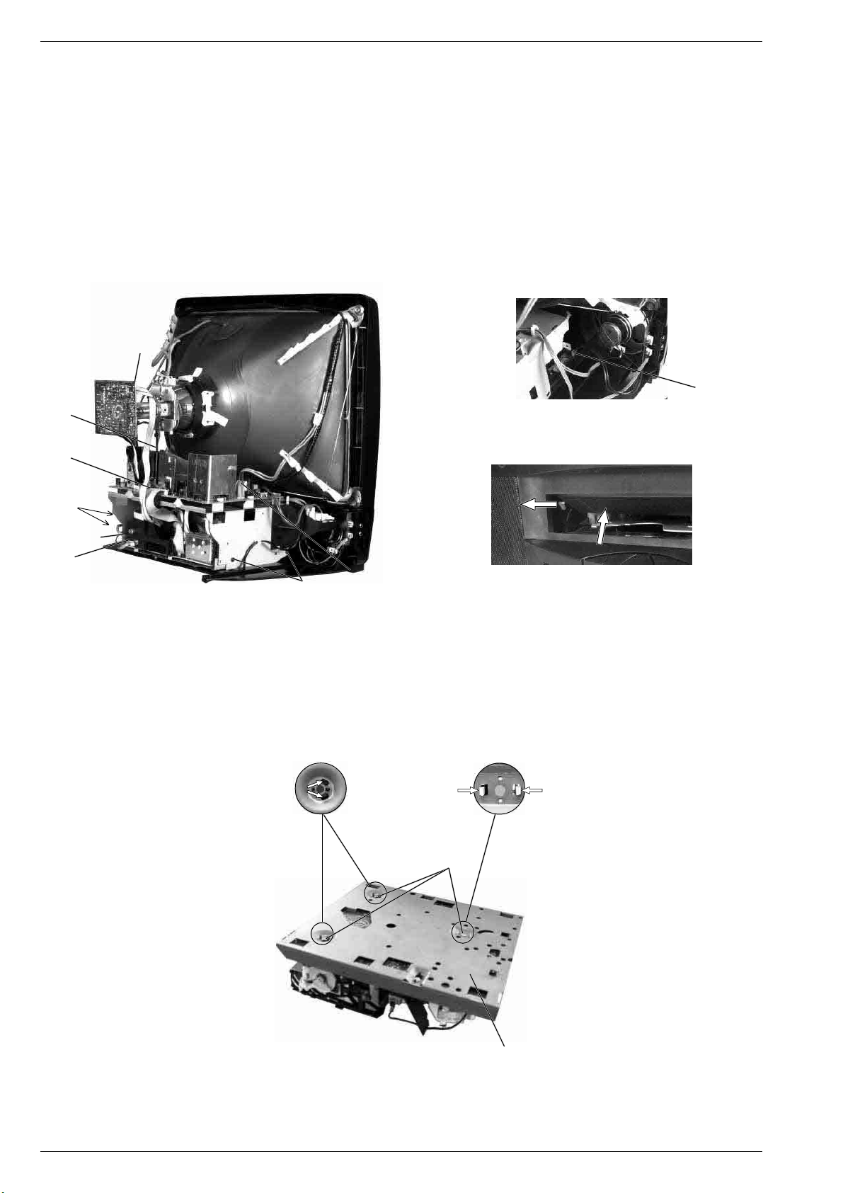
Allgemeiner Teil / General Section TVR 3710 …, TVR 5100 …, TVR 5500 …
1.3 Videoteil ausbauen
– 4 Schrauben (Pos. 12) entfernen (Fig. 6).
– Stecker 1921, 1922 und 1923 (Fig. 6) vom Leistungs-Chassis
abziehen.
– Stecker 1967 (Fig. 6) von der Bildrohrplatte abziehen.
– Leistungs-Chassis und Videoteil mit Montageträger so weit zur
Geräterückseite schieben, daß der Stecker 1918 (Fig. 7) auf dem
Signal-Chassis zugänglich ist.
Stecker 1918 vom Signal-Chassis abziehen.
– Stecker 1971 (Option) vom Signal-Chassis abziehen (Fig. 6).
– Lautsprecherstecker 1914 und 1970 (Option) abziehen (Fig. 6).
– Videoteil vorsichtig anheben und nach hinten herausziehen.
Hinweis zum Zusammenbau: Beim Einschieben des Videoteils in
das Gerät ist die Cassettenklappe so nach innen zu drücken, daß
der Hebel vor der Cassettenklappe ist (Fig. 8).
1967
1925
1921
1922
1923
1.3 Removing the Video Unit
– Undo 4 screws (Pos. 12, Fig. 6).
– Unplug the connectors 1921, 1922 and 1923 (Fig. 6) on the Power
Chassis.
– Unplug the connector 1967 (Fig. 6) on the Tube PCB.
– Push the Power Chassis and the Video Unit towards the back of the
TVR so that the connector 1918 on the Signal Chassis (Fig. 7) is
accessible.
Unplug the connector 1918 from the Signal Chassis.
– Pull out the connector 1971 (option) from the Signal Chassis (Fig. 6).
– Unplug the loudspeaker connectors 1914 and 1970 (option, Fig. 6).
– Raise the Video Unit carefully by a small amount and take it out
towards the back.
Note on re-assembling: When pushing the Video Unit into the TVR
push the cassette flap inwards so that the lever is in front of the
cassette flap (Fig. 8).
1918
Fig. 7
12
1971 (Option)
1914
1970 (Option)
Fig. 6
1.3.1 Laufwerk ausbauen
– Steckverbindungen zwischen Signal-Chassis und Laufwerk lösen.
– 3 Schrauben (Fig. 9, Pos. 31) herausdrehen.
– Rastnasen der Laufwerkhalter ausrasten (Fig. 9).
– Abschirmblech (Pos. 20) mit dem Signal-Chassis abnehmen.
Fig. 9
12
1924
!
Fig. 8
1.3.1 Removing the Drive Mechanism
– Unplug the connections between the Signal Chassis and the drive
mechanism.
– Undo 3 screws (Fig. 9, Pos. 31).
– Release the locking lugs of the drive mechanism holders (Fig. 9).
– Remove the metal screen (Pos. 20) together with the Signal Chassis
31
20
1 - 10 GRUNDIG Service
Page 12
TVR 3710 …, TVR 5100 …, TVR 5500 … Allgemeiner Teil / General Section
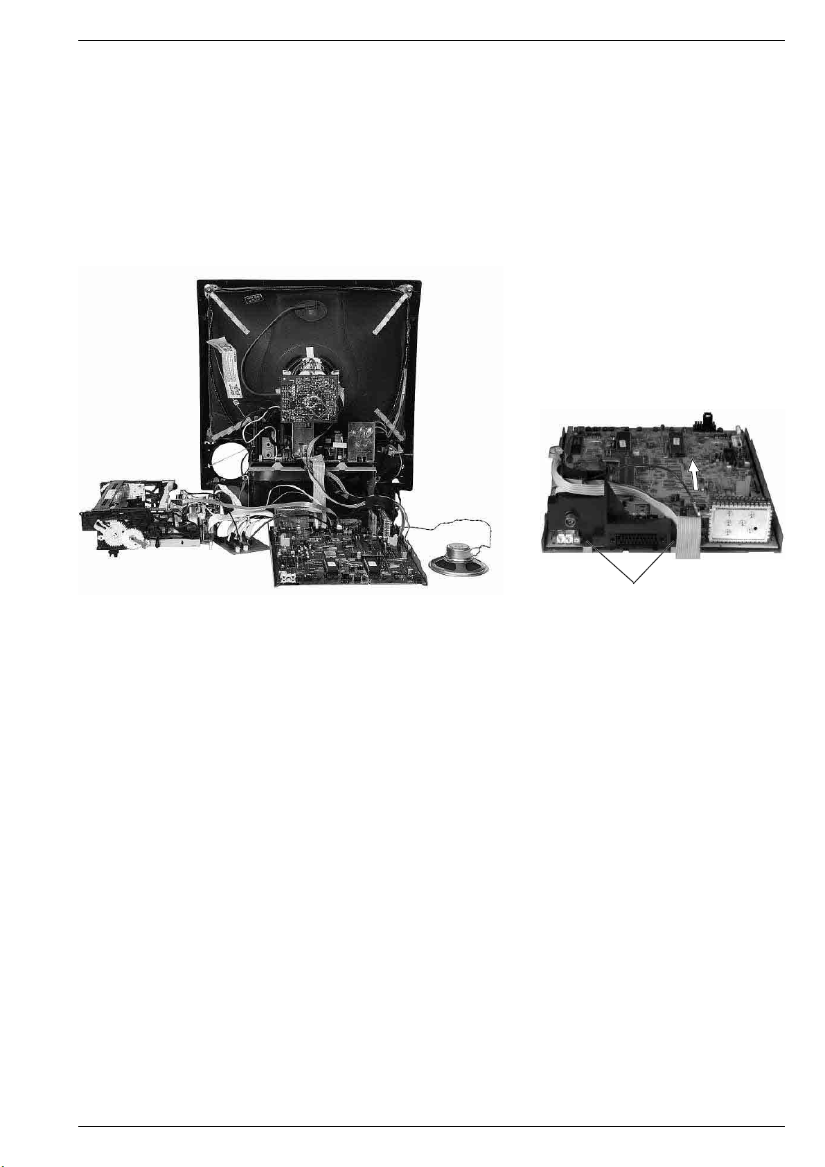
Betrieb des Gerätes mit ausgebautem Laufwerk (Fig. 10)
– Mit dem Kabeladapter (Sach-Nr. 75988-009.79) die Steckverbin-
dungen des Laufwerks mit dem Signal-Chassis verbinden.
– Stecker 1921, 1922 und 1923 mit dem Leistungs-Chassis und
Stecker 1967 mit der Bildrohrplatte verbinden.
– Gegebenenfalls Lautsprecher-Befestigungsfeder lösen und Laut-
sprecher herausnehmen. Lautsprecherstecker 1914 und 1970 (Option) anschließen.
Achtung: Laufwerk nur in horizontaler Lage betreiben.
1.3.2 Signal-Chassis ausbauen
– Laufwerk ausbauen (siehe Pkt.1.3.1).
– 2 Schrauben (Pos. 12, Fig. 11) herausdrehen.
– Signal-Chassis in Pfeilrichtung (Fig. 11) schieben und nach oben
abnehmen.
Operating the dismantled drive mechanism (Fig. 10)
– Use the cable adapter (part no. 75988-009.79) to connect the
connectors of the drive mechanism to the Signal Chassis.
– Connect the connectors 1921, 1922 and 1923 with the Power
Chassis and connector 1967 with the Tube PCB.
– If necessary detach the loudspeaker fastening spring and take out
the loudspeaker. Connect the loudspeaker connectors 1914 and
1970 (option).
Attention: Operate the drive mechanism only in horizontal position.
1.3.2 Removing the Signal Chassis
– Dismantle the drive mechanism (see chapter 1.3.1).
– Undo 2 screws (Pos. 12, Fig. 11).
– Push the Signal Chassis in the direction of the arrow (Fig. 11) and
remove it towards the top.
Kabeladapter / Extension cable kit
Sach-Nr / part no. 75988-009.79
Fig. 10 Fig. 11
2. Wichtige Masseverbindungen!
Beim Zusammenbau des Gerätes ist darauf zu achten, daß die
Masseverbindungen zwischen den einzelnen Bausteinen gewährleistet sind.
3. Durchführen von Messungen
Bei Messungen mit dem Oszilloskop an Halbleitern sollten Sie nur
Tastköpfe mit 10:1 - Teiler verwenden. Außerdem ist zu beachten, daß
nach vorheriger Messung mit AC-Kopplung, der Koppelkondensator
des Oszilloskops aufgeladen sein kann. Durch die Entladung über das
Meßobjekt können diese Bauteile beschädigt werden.
4. Meßwerte und Oszillogramme
Bei den in den Schaltplänen und Oszillogrammen angegebenen
Meßwerten handelt es sich um Näherungswerte!
2. WARNING: Chassis connections!
When re-assembling make sure that the ground connections between
the boards are fitted.
3. Carrying out Measurements
When making measurements on semi-conductors with an oscilloscope, ensure that the test probe is set to 10:1 dividing factor. Further,
please note that, if the previous measurement is made on AC input, the
coupling capacitor in the oscilloscope will be charged. Discharge via
the item being checked can damage components.
4. Measured Values and Oscillograms
The measured values given in the circuit diagrams and oscillograms
are approximates!
12
GRUNDIG Service 1 - 11
Page 13
Allgemeiner Teil / General Section TVR 3710 …, TVR 5100 …, TVR 5500 …
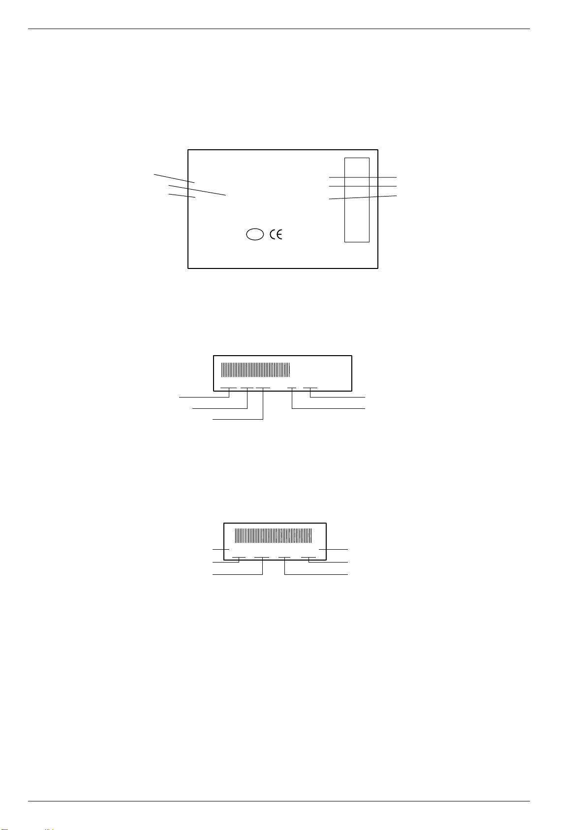
5. Codeaufkleber
Alle wichtigen Komponenten des Gerätes (Laufwerk / Platinen) sind
mit einem Codeaufkleber versehen. Diese Aufkleber beinhalten die
Typenbezeichnung und Produktionsdaten (Seriennummer,
Produktioncode, Produktionsdatum, …).
Typenschild des Gerätes
Hinweis:
Bei wichtigen Änderungen erhöht sich der Produktionscode um eins.
1
Bestellnummer / Order number
Produktionsdatum / Production date
Produktionscode / Production code
Laufwerks-Codeaufkleber
Hinweis:
Der Produktionscode und die Seriennummer auf dem Codeaufkleber
des Laufwerks muß nicht mit dem Produktionscode und der Seriennummer auf dem Typenschild übereinstimmen.
TYPE
G.CC 26-75
VN37 046
220-240V ~ 50Hz 48Watt
(D.M.26-3-1992)
F L A
EIGENSICHERE KATHODENSTRAHLRÖHRE NACH ANLAGE III DER RÖNTGENVERORDNUNG,
BESCHLEUNIGUNGSSPANNUNG MAX. 25KV 0,8mA
INTRINSICALLY SAFE CATHODE RAY TUBE AS SET FORTH IN ANNEX III OF THE RADIATION
EMITTING DEVICES REGULATIONS, ACCELERATING VOLTAGE MAX 25KV 0.8mA
ÖVE
5. Code Labels
All important components of the video recorder (drive mechanism /
printed circuit boards) are provided with a code label. These adhesive
labels indicate the type of product and the production data (serial
number, production code, date of production, …).
Type Plate
Advice:
Important changes are indicated by increasing the change code by
one.
TVR 3710
TVP 762
SER.NR. 100547
D
23kV
Code Label on the Drive Mechanism
Advice:
The production code and the serial number on the code label of the
drive mechanism do not necessarily agree with the production code
and the serial number on the type plate.
UNDER LICENSE FROM
BY GEMSTAR DEVELOPMENT CORP.
GEMSTAR DEVELOPMENT CORPORATION
SHOW VIEW SYSTEMS IS MANUFACTURED
SHOW VIEW IS A TRADEMARK APPLIED FOR
Gerätetype / Type of product
Fernbedienung / Remote Control
Seriennummer / Serial number
09642418222009
82220099 09642 T-P 2/0 9620 10WD41
Seriennummer / Serial number
Fabrikcode / Factory code number
Laufwerkstype / Type of drive mechanism
Platinen-Codeaufkleber
Hinweis:
Der Produktionscode ist nicht generell aufgedruckt. Bei wichtigen
Änderungen erhöht sich die letzte Ziffer der Fabrikscodenummer
(Punktnummer).
Platinenbezeichnung / Name of PCB
Fabrikscode / Factory code number
Produktionsdatum / Production date
PLSP14B 27599-101.23
65284 KW606 VN05 123456
Produktionscode / Production code
Produktionsdatum / Production date
Code Label on the Printed Circuit Boards
Advice:
The production code is not generally printed on the label. Important
changes are indicated by increasing the last figure of the factory code
by one (figure following the point).
Sach-Nummer / Part number
Seriennummer / Serial number
Produktionscode / Production code
1 - 12 GRUNDIG Service
Page 14
TVR 3710 …, TVR 5100 …, TVR 5500 … Allgemeiner Teil / General Section
Servicetestprogramm
Aufruf, Ebenenkontrolle und Beenden des Servicetestprogrammes
Das Servicetestprogramm darf in den folgenden Betriebsarten nicht
gestartet werden:
– Sendersuchlauf
– Install
– Uhr und Cassettenlänge einstellen
Während dem Betrieb des Servicetestprogramms bleiben alle
Laufwerksfunktionen voll einsatzbereit.
Aufruf des Servicetestprogramms
–Die Tasten ¢■(STOP) auf der Fernbedienung und ¢e(Wieder-
gabe) am Gerät in dieser Reihenfolge drücken und für mindestens
5s gedrückt halten.
– Auf dem Monitor erscheinen anschließend die Werte der Service-
ebene "SERVICE STATUS" (siehe Pkt. 1.).
Aufruf der Serviceebene "SERVICE CONTROL"
– In die Serviceebene "SERVICE CONTROL" gelangt man über die
Serviceebene "SERVICE STATUS" durch das Drücken der Taste
G auf der Fernbedienung.
– Auf dem Monitor erscheinen anschließend die Werte und Funktio-
nen der Serviceebene "SERVICE CONTROL" (siehe Pkt. 2.).
Aus- und Einblenden des Servicetestprogramms
– Das Aus- und Einblenden des Servicetestprogramms ist durch das
Drücken der Taste . auf der Fernbedienung möglich. Auf dem
Monitor erscheinen nach dem Einblenden die Werte der Serviceebene "SERVICE STATUS" (siehe Pkt. 1.).
Beenden des Servicetestprogramms
–Taste b (Standby) drücken oder Gerät vom Netz trennen.
Service Test Programme
Calling up, Checking the Levels of and Terminating the Service
Test Programme
The service test programme must not be called up from the following
operating modes:
– station search
– install
– setting the clock and cassette length
During the service test programme, the VCR remains fully operational
for all tape drive functions.
Calling up the Service Test Programme
– Press the ¢■(STOP) button on the remote control and then the
(play) button on the video recorder and hold them down for at
¢e
least 5 seconds.
– The monitor will then show the values of the "SERVICE STATUS"
level (see point 1).
Calling up the "SERVICE CONTROL" Level
– The "SERVICE CONTROL" level can be reached via the
"SERVICE STATUS" level by pressing the G button on the
remote control.
– The values and functions of the "SERVICE CONTROL" level are
then displayed on the monitor (see point 2.).
Fading the Service Test Programme In or Out
– The Service Test Programme can be faded in or out by pressing the
button on the remote control. On fading in the monitor shows the
.
values of the "SERVICE STATUS" level (see point 1).
Terminating the Service Test Programme:
–Press the b (Standby) button or disconnect the mains.
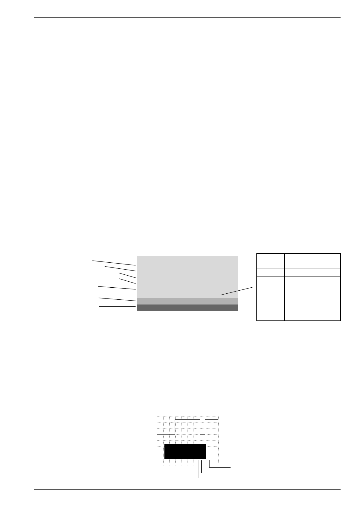
1. Serviceebene "SERVICE STATUS"
Nach dem Aufruf des Servicetestprogramms werden am Bildschirm
die Werte der Serviceebene "SERVICE STATUS" angezeigt.
Laufwerksensoren / Tape Deck Sensors
– Init Schalter / Init Switch
– Fädeltacho / Threading Tacho
– Bandende/-anfang / Tape End/Begin
– Aufnahmesperre / Record Protection
– Wickeltacho Links/Rechts /
Reel Tacho left/right
Serviceebene / Service Level
"SERVICE CONTROL"
Maskennummern / Mask No.
– Bedienrechner / Keyboard Control µC
(IC7801) "PTCG1-1"
– TVC (IC7410) "BTVD2-0P"
Kontrolle der Laufwerksensoren und der Laufwerkstellung
Zur Kontrolle der Laufwerksensoren (Init Schalter, Fädeltacho, Bandanfang, Bandende, Aufnahmesperre, Wickeltacho Links / Rechts)
werden auf dem Monitor die Betriebszustände mit einer Digitalstelle
angezeigt. Mit jeder Betätigung der Sensoren ändern sich die Werte
der Anzeige.
Der Code für die Laufwerkstellung (siehe Tabelle) gibt die Position des
Cassettenschachts und der Fädelschlitten an.
Laufwerkstellung und Funktion des Init Schalters
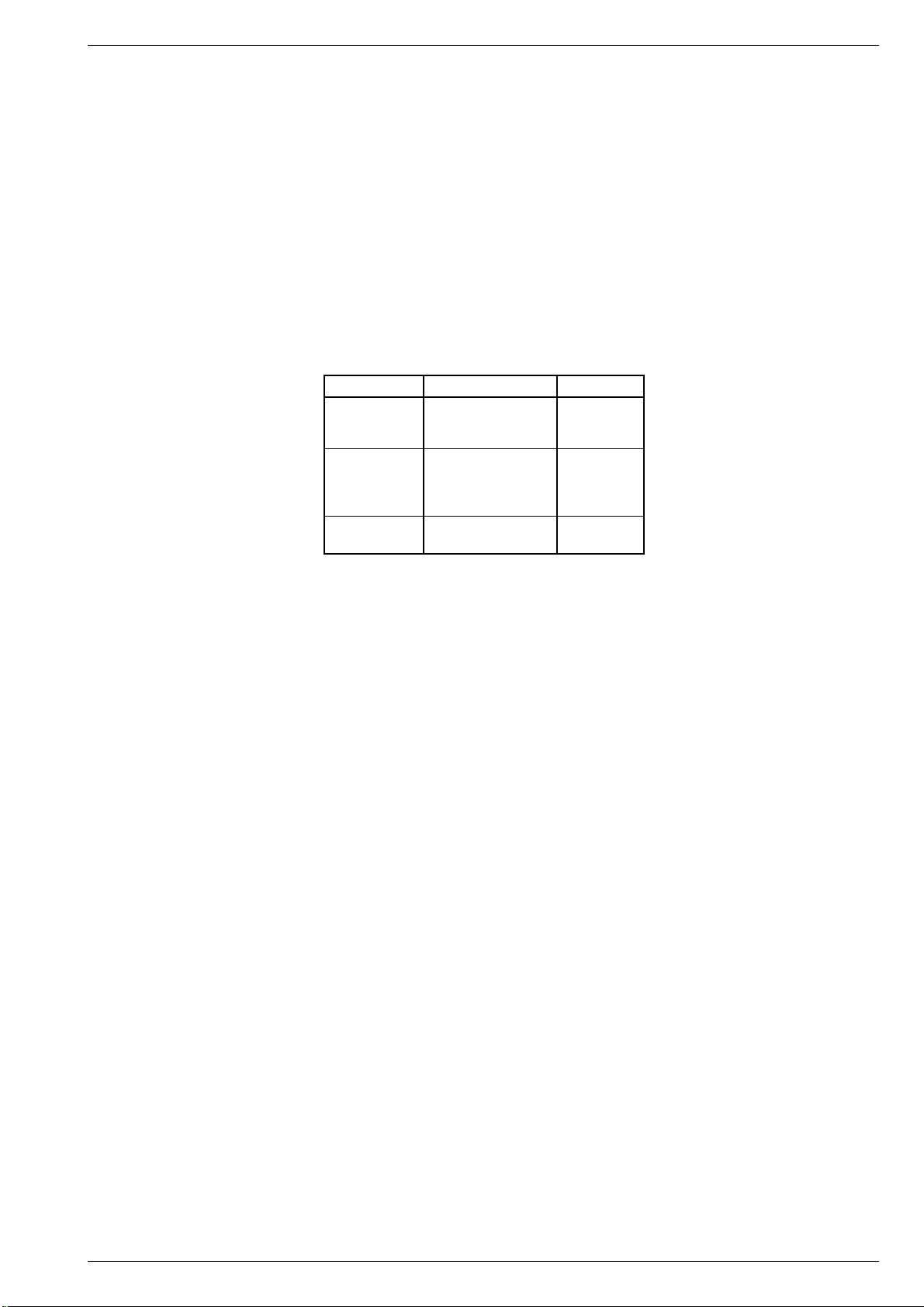
Das Diagramm zeigt die Funktion des Init-Schalters in Abhängigkeit
von der Stellung des Laufwerks. Dafür ist die Anzahl der Fädeltachoimpulse (FTA) wichtig.
Diese Impulse erzeugt
der Fädeltachogeber
(Flügelrad), der mechanisch mit dem Fädelmotor verbunden ist.
A: AC, 2V/Div, 0,5s/Div
B: AC, 2V/Div, 0,5s/Div
SERVICE STATUSSERVICE STATUS
INIT SWITCHINIT SWITCH 00
LOADING PULSELOADING PULSE 00
TAPE BEGIN / ENDTAPE BEGIN / END 0 10 1
RECORD PROTECTRECORD PROTECT 00
REEL PULSE L / RREEL PULSE L / R 0 10 1
TAPE DECK STATUSTAPE DECK STATUS 214214
SERVICE CONTROLSERVICE CONTROL
UP: PTCG1–1 BTVD2–0P UP: PTCG1–1 BTVD2–0P
A
1. The "SERVICE STATUS" Level
On calling up the Service Test Programme the monitor shows the
values of the "SERVICE STATUS" level.
Code Laufwerkstellung /
5…9
100…102
212…216
237…239
Checking the Tape Deck Sensors and the Tape Deck Position
For checking the tape deck sensors (Init switch, threading tacho, tape
beginning, tape end, record protection, reel tacho left / right) the
operating positions are indicated on the monitor by means of one digit.
The indicated value changes with each operation of a sensor.
The code for the tape deck status (see table) indicates the position of
the cassette compartment and the threading roller units.
Tape Deck Position and Function of the Init Switch
The diagram shows the function of the Init switch dependent on the
tape deck position. For this, the number of the threading tacho pulses
(FTA) is important. These signals are generated by the threading tacho
Init Schalter / Init switch
Tape Deck Position
Auswurf / Eject
Ausgefädelt-Stop /
Stop threaded out
Wiedergabeposition /
Play position
Wiedergabe rückwärts /
Play reverse
generator (butterfly sensor) which is mechanically connected with the
threading motor.
Fädeltacho-Impuls (FTA)
B
Cassette eingeschoben / Cassette in
Cassette unten / Cassette down Band halb eingefädelt / half the tape threaded in
GRUNDIG Service 1 - 13
Threading pulse (FTA)
Wiedergabe / Play
Band eingefädelt / tape threaded in
Page 15
Allgemeiner Teil / General Section TVR 3710 …, TVR 5100 …, TVR 5500 …
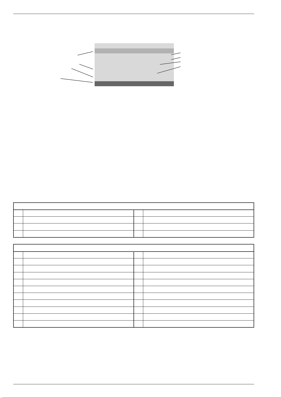
2. Serviceebene "SERVICE CONTROL"
Nach dem Aufruf der Serviceebene "SERVICE CONTROL" werden
am Bildschirm z.B. folgende Werte und Funktionen angezeigt.
SERVICE CONTROLSERVICE CONTROL
Funktionen / Functions
– EEPROM löschen / EEPROM clear
– Kopfradlagengeber / Head gap pos. indicator
– Tunerselektion /Tuner selection
Steuer- und Eingabetasten /
Control and entry keys
2.1 Löschen des EEPROMs IC7813
Achtung: Mit dieser Funktion wird das EEPROM gelöscht und initia-
lisiert (ausgenommen Laufwerkparameter und Optionen).
Dabei wird der gesamte kundenspezifische Senderspeicher und alle
Timer-Daten gelöscht. Die Grundeinstellungen für Kontrast, Helligkeit,
Bildschärfe, Farbsättigung und Lautstärke werden geladen.
Aufruf der Löschfunktion
–Mit den Tasten ]| der Fernbedienung die Zeile "RAM CLEAR"
anwählen.
– Taste
Hinweis: Nach dem Tausch des EEPROMs muß dieses gelöscht und
initialisiert werden. Zusätzlich ist der Abgleich "Kopfradlagengeber
(GAP)" durchzuführen (siehe Kap. 3 - Abgleich der Ablaufsteuerung).
2.2 Fehlercodes und Fehlerstatus
Die drei zuletzt aufgetretenen Fehlercode- und Fehlerstatus-Meldungen werden gespeichert und bleiben auch dann erhalten, wenn das
Gerät vom Netz getrennt wird.
Löschen der Fehlercodes und Fehlerstatus
–Mit den Tasten ]| der Fernbedienung die Zeile "ERROR" oder
"ERROR STATUS" anwählen.
– Taste
CL auf der Fernbedienung drücken.
m
CL auf der Fernbedienung drücken.
m
RAM CLEARRAM CLEAR
ERRORERROR 0000 0000 F0F0
ERROR STATUSERROR STATUS 0000 0000 3636
OPTIONSOPTIONS 5626856268
GAP POSITIONGAP POSITION
HEAD HOURSHEAD HOURS 19801980
DISPLAY TUNERDISPLAY TUNER TVTV
MN
2. The "SERVICE CONTROL"Level
On calling up the "SERVICE CONTROL" level the following values for
example are shown on the screen.
Fehlercodes / Error Codes
Fehlerstatus / Error Status
Geräte-Codenummer / TVR Code Number
Betriebsstundenzähler / Operating Hours
CLEARCLEAR
2.1 Clearing the EEPROM IC7813
Attention: This function clears and initializes the EEPROM (with the
exception of tape deck parameters and options).
The customised station memory and the timer data are also cleared.
The basic settings for contrast, brightness, picture sharpness, colour
saturation and volume level are loaded.
Calling up the Clear Function
– Select the "RAM CLEAR" line with the ]| buttons on the remote
control.
– Press the
Note:
The EEPROM must be cleared and initialized after replacement.
Additionally the "headwheel position indicator (GAP)" must be realigned (see chapter 3 - Adjustment of the System Control).
2.2 Error Codes and Error Status
The three error codes and error status that occurred last are stored and
are saved even if the VCR is disconnected from the mains.
Clearing the Error Codes and Error Status
– With the ]| buttons on the remote control select "ERROR" or
"ERROR STATUS".
– Press the
CL button on the remote control.
m
CL button on the remote control.
m
Laufwerk-Fehlercode / Drive Mechanism Error Code
00
Kein Fehler / No error
F0
Fädelfehler / Threading error
F1
Kein Capstantacho / No capstan tacho
F2
Band gerissen / Tape torn
Laufwerk-Fehlerstatus / Tape Deck Error Status
00
Bereitschaft - kein Fehler / Standby - no error
0C
Bereitschaft / Standby
1F
Wiedergabe rückwärts (3-fach) / Play reverse (3x)
20
Cassettenschacht oben / Lift up
21
Cassettenschacht unten / Lift down
29
Standbild / Still
2A
Bildsuchlauf vorwärts (2- / 3-fach) / Picture search forward (2x / 3x)
2C
Bildsuchlauf rückwärts / Picture search reverse
2E
Bildsuchlauf vorwärts / Picture search forward
2F
Wiedergabe rückwärts / Play reverse
30
Pause
F3
Fehlender Wickeltacho links / Missing left reel tacho (Option)
F4
Fehlender Wickeltacho rechts / Missing right reel tacho
F5
Kopfscheibenmotorfehler / Headwheel motor error
32
Rücklauf / Rewind
34
Vorlauf / Wind
35
Wiedergabe / Play
36
Stop
37
Aufnahme / Record
70
Nächster Index / Next index
71
Vorheriger Index / Previous index
80
Stop - Bandanfang / Stop - Tape Begin
81
Stop - Bandende / Stop - Tape End
C5
Bereitschaft - Schacht oben / Standby - eject
EE
Aufnahme - Pause / Record - Pause
1 - 14 GRUNDIG Service
Page 16
TVR 3710 …, TVR 5100 …, TVR 5500 … Allgemeiner Teil / General Section
Überwachung der Laufwerksfunktionen
Für die Überwachung der Laufwerksfunktionen sind am Laufwerk
Sensoren angebracht. Diese liefern entsprechend der Gerätefunktion
folgende Tachosignale:
– WTR – Wickelteller rechts
– FTA – Fädeltacho
– FG – Capstanmotor
– PG/FG – Kopfscheibenmotor.
Fehlt bei der Ansteuerung des Laufwerks ein Tachosignal, dann
versucht das Gerät, den Cassettenschacht in die Stellung "EJECT" zu
bringen.
2.3 Geräte-Optionscode
–Mit den Tasten ]| der Fernbedienung die Zeile "OPTION CODE"
anwählen.
– 5-stelligen Optionscode, siehe Geräte-Codenummern (z.B. 56268
bei TVR 5500) mit der Fernbedienung eingeben.
Achtung: Nur bei richtiger Optionscode-Eingabe sind alle Geräte-
funktionen gewährleistet.
– Taste O auf der Fernbedienung drücken.
Best-Nr. / Order No. Option-Code
TVR 3710 G.CC 26-75
TVR 3710 FR G.CC 29-75 FB
TVR 3710 GB G.CC 28-75 GB
TVR 5100 G.CC 30-75
TVR 5100 G.CC 31-75
TVR 5100 G.CC 32-75
TVR 5100 FR G.CC 33-75 FB
TVR 5500 G.CC 34-75
TVR 5500 FR G.CC 36-75 FB
Monitoring the Tape Deck Functions
For monitoring the tape deck functions the tape deck is fitted with
sensors which supply the following tacho signals according to the
functions:
– WTR – reel right
– FTA – threading tacho
– FG – capstan motor
– PG/FG – headwheel motor
When one tacho pulse is missing during the operation of the tape deck,
the VCR tries to move the cassette compartment to the "EJECT"
position.
2.3 Option Code
– With the ]| buttons on the remote control, select the line
"OPTION CODE".
– Enter the 5-digit option code - see code number (e.g. 56268 for
TVR 5500) - on the remote control.
Attention: Execution of all TVR functions is only ensured if the
option code is correctly entered.
– Press the O button on the remote control.
23500
57280
16104
03020
04076
04076
00448
56268
57312
2.4 Kopfradlagengeber (GAP)
Hinweis: Nach dem Tausch des EEPROMs IC7813 oder der Kopf-
scheibe ist der Abgleich "Kopfradlagengeber (GAP)" durchzuführen
(siehe Kap. 3 - Abgleich der Ablaufsteuerung).
2.5 Betriebsstundenzähler
Der Betriebsstundenzähler gibt die Betriebsstunden der Kopfscheibe
an.
2.6 Tunerselektion
Bei Geräten mit 2 Tunern wird der Tuner 1702 für den TV-Betrieb
verwendet und der Tuner 1301 für die Video-Aufnahme.
Reparaturtip: Mit der Tunerselektion besteht die Möglichkeit, das Bild
und den Ton des Tuners 1301 in den TV-Signalweg einzuspeisen und
wiederzugeben.
Aktivierung der Tuner
–Mit den Tasten ]| der Fernbedienung die Zeile "DISPLAY
TUNER" anwählen.
– Durch das Drücken der Taste x oder c auf der Fernbedienung
kann zwischen den beiden Tunern hin- und hergeschaltet werden.
Auf dem Bildschirm wird der aktive Tuner (TV / VCR) angezeigt.
Hinweis:
– Bei der Aktivierung des Tuners 1301 wird die Tuner-Regelspannung
nicht ausgewertet.
– Bei der Wiedergabe einer Cassette wird nur der Signalweg zur TV-
Signalelektronik freigegeben, wenn der Tuner 1301 des Video-Teils
angewählt ist.
– Nach dem Beenden des Servicetestprogrammes ist die Grundein-
stellung (Tuner 1702 für TV-Betrieb und Tuner 1301 für Video-
Betrieb) wieder aktiv.
2.4 Headwheel Position Indicator (GAP)
Note: After the EEPROM IC7813 or the headwheel has been replaced
the "headwheel position indicator (GAP)" must be realigned (see
chapter 3 - Adjustment of the System Control).
2.5 Operating Hours Meter
The operating hours meter indicates the number of hours the headwheel has been rotating.
2.6 Tuner Selection
In models fitted with 2 tuners, tuner 1702 is used for TV operation and
tuner 1301 for video signal recording.
Repair tip: With the tuner selection function it is possible to feed picture
and sound of tuner 1301 into the TV signal path and to play these
signals back.
Activating the Tuners
– With the ]| buttons on the remote control, select the line
"DISPLAY TUNER".
– Pressing the x or c button on the remote control allows to switch
over between the two tuners.
The active tuner (TV / VCR) is indicated on the screen.
Note:
– On activation of tuner 1301 the tuner control voltage will not be
evaluated.
– On playback of a cassette, only the signal path to the TV Signal
Electronics is released if tuner 1301 of the video unit is selected.
– On termination of the Service Test Programme, the default setting
(tuner 1702 for TV operation and tuner 1301 for video operation) is
reactivated.
GRUNDIG Service 1 - 15
Page 17

Allgemeiner Teil / General Section TVR 3710 …, TVR 5100 …, TVR 5500 …
Notizen / Notes
1 - 16 GRUNDIG Service
Page 18
IC7310-(1)
IC7310 int.
IC7310 int.
IC7310-(11)
IC7310 int.
IC7310-(3)
IC7310-(1)
V
cc
V
cc prot
V
cc start
V
ref
V
dis2
V
dis1
V
pin11
UVL01
V
ovp out
Output
I
cc
17mA
0,3mA
No-Take Over
Re-Start
Start-Up
Normal Mode
Loop Failure
>2ms
t
t
t
t
t
t
t
TVR 3710 …, TVR 5100 …,TVR 5500 … Beschreibung
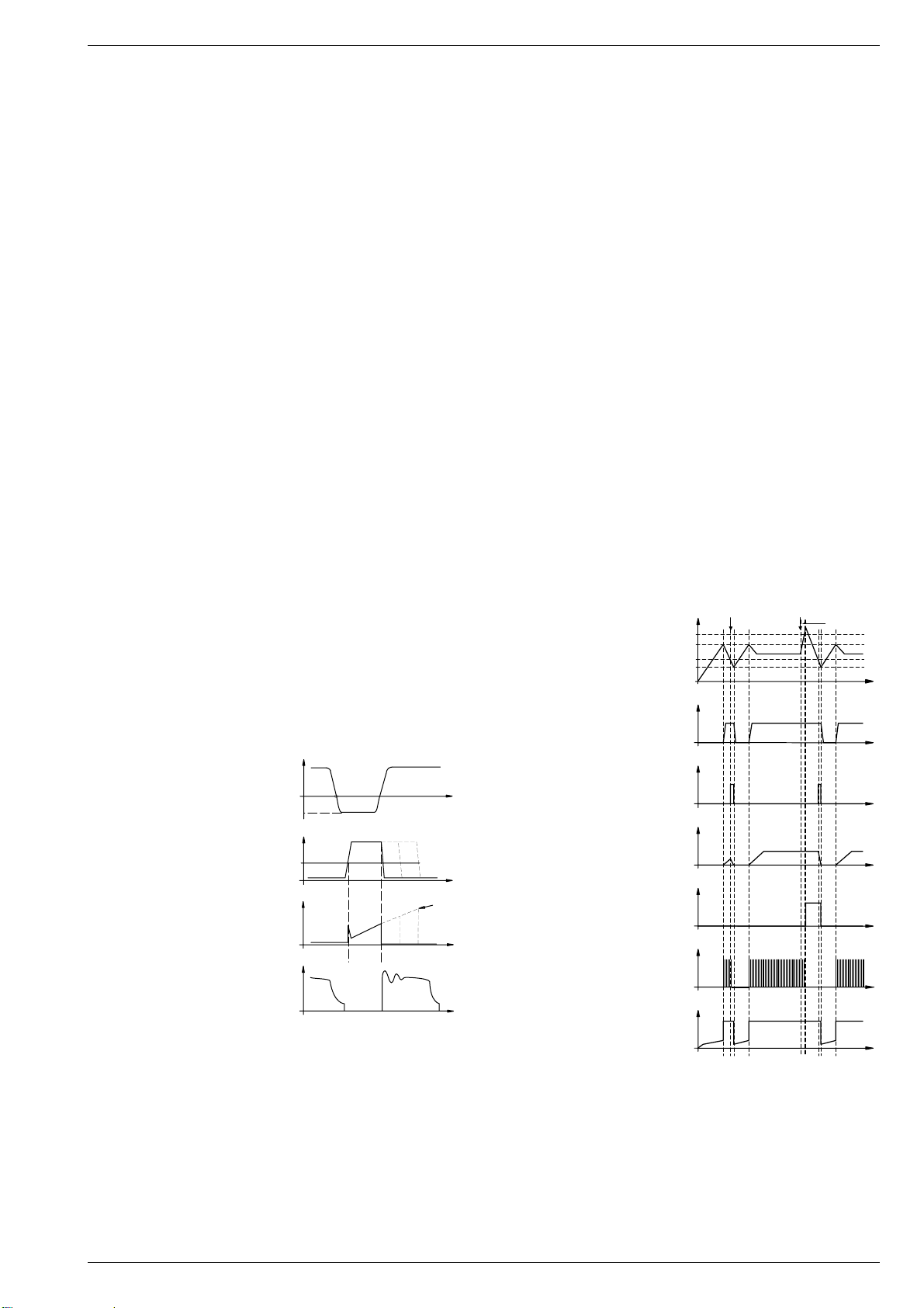
Ist die gesamte im Trafo gespeicherte Energie an die Last abgegeben
Beschreibung
j
und das magnetische Feld abgeklungen, so fallen die Spannungen an
den Sekundärwicklungen unter 0V. Diese Nulldurchgänge erkennt
IC7310 an Pin 8. Der Schalttransistor T7330 wird erneut durch-
1. Leistungs-Chassis (PLSP)
1.1 Leistungs-Chassis – Netzteil
Typische Daten:
Netzspannung: 196…265V~
Netzfrequenz: 45…65Hz
Maximale Leistung: 130W
Schaltfrequenz: 30…85kHz
Wirkungsgrad: 80% bei maximaler Leistung
Alle Ausgänge sind kurzschlußgeschützt
Sperrwandlerprinzip
Während der Leitphase des Schalttransistors T7330 wird Energie vom
Netz in den Trafo übertragen. Diese Energie wird in der Sperrphase an
die Last abgegeben. Mittels der Einschaltzeit und der Frequenz wird
die Energie, die in jedem Zyklus übertragen wird, so geregelt, daß die
Ausgangsspannungen unabhängig von den Änderungen der Last
oder der Eingangsspannung sind. Die Regelung und Ansteuerung des
Schalttransistors übernimmt IC7310.
Verschiedene Lastfälle
– Leerlauf (STANDBY-Betrieb / TIMER-Aufnahmebereitschaft):
Der IC7310 erkennt über die Lastaufnahme den Leerlaufbetrieb und
regelt die Frequenz auf ca. 30kHz herunter, um die Schaltverluste
am Power-MOS-Transistor T7330 zu minimieren.
– Normalbetrieb (Regelbereich):
Die Schaltfrequenz sinkt mit steigender Last. Das Tastverhältnis
wird im wesentlichen durch die Netzspannung kontrolliert. Die
Ausgangsspannungen sind geringfügig lastabhängig.
– Umkehrpunkt:
Bei diesem Punkt der Ausgangscharakteristik ist die übertragene
Leistung am höchsten.
– Überlast:
Das Netzteil arbeitet im Burst-Mode, d.h. die Energie in jedem
Zyklus wird begrenzt, so daß die Ausgangsleistung gering ist.
Schaltungsbeschreibung
Die Netzspannung wird mit dem Brückengleichrichter D6313…D6316
gleichgerichtet und mit C2315 gesiebt. Mit L5311 werden Störimpulse
des Netzteils vom Netz ferngehalten. Während der Anlaufphase erfolgt
die Spannungsversorgung des IC7310 an Pin 1 über R3331 und C2310.
Nach der Anlaufphase wird die Spannungsversorgung über die Trafowicklung 4 / 3 und D6334 übernommen. Die Induktivität der
Primärwicklung 1 / 5…7 bestimmt die Eigenfrequenz des
Schaltnetzteils im Normalbetrieb. Die maximale Frequenz
wird mit C2327 an IC7310-(10)
vorgegeben.
Während der Einschaltzeit des
Schalttransistors T7330 fließt
der Strom der gleichgerichteten
Netzspannung über die Primärwicklung des Trafos (Kontakte
1 / 5…7), T7330 und R3334,
R3335 nach Masse (primärseitig). Da die Spannung am Kontakt 1 des Trafos annähernd
konstant ist, steigt der Strom
linear. Seine Stärke ist abhängig von der Netzspannung und der Induktivität der Primärwicklung. Im
Trafo bildet sich ein magnetisches Feld, welches einer bestimmten
Energiemenge entspricht. Die Sekundärspannungen sind in dieser
Phase so gepolt, daß die Dioden sperren. Über die Widerstände R3334,
R3335, R3359 wird dem IC7310 an Pin 7 eine Spannungsabbildung des
Primärstroms zugeführt. Übersteigt diese Spannung einen bestimmten
Wert, der abhängig ist von der Regelspannung an IC7310-(14), wird der
Schalttransistor T7330 abgeschaltet. Dieser Vorgang wiederholt sich
bei jedem Einschalten des Schalttransistors T7330.
Nach dem Abschalten des Schalttransistors T7330 wird keine Energie
in den Trafo übertragen. Die im Trafo gespeicherte Energie baut sich
nun über die Sekundärwicklungen ab. Durch die Umkehrung der
Polarität der Spannungen am Trafo fließt ein Strom durch die Sekundärwicklungen des Trafos, durch die Dioden, Elkos und die Last.
GRUNDIG Service 2 - 1
+U
IC7310-(8)
U
IC7310-(3)
T7330
U
T7330
-U
GS
Dmax
I
D
DS
I
Point of Reversal
geschaltet und ein neuer Zyklus beginnt.
Die Regelung des Schaltnetzteiles erfolgt durch Verändern der Leitphase des Schalttransistors, so daß entweder mehr oder weniger
Energie vom Netz in den Trafo übertragen wird. Die Regelinformation
kommt von der Trafowicklung 3 / 4 über D6335 / C2337 und
R3356…R3358 zum Pin 14 des IC7310. Der Verstärker "ERROR
AMP" IC7310 vergleicht diese Spannung mit der internen 2,5VReferenzspannung. Dieser Vergleich verändert den Pegel, mit dem
die Spannung an Pin 7 des IC7310 (Primärstromabbildung) verglichen
wird.
In der Sperrphase des T7330 begrenzen C2332 / D6332 und C2331 /
R3345 die Spannungsspitzen auf der Primärseite.
Zur Vermeidung statischer Aufladungen besitzt das Gate des Schalttransistors T7330 den Pull Down-Widerstand R3339. Die Spannung
am Pin 5 des IC7310 wird zur Rückwärtsregelung (FOLD BACK)
benötigt.
Die maximal entnehmbare Sekundärleistung bestimmen R3334 /
R3335. Das Netzteil geht ab 1V (typisch) an IC7310-(7) in den
Umkehrpunkt.
Die Beschaltung an Pin 11 ist eine Option des IC7310. Mittels C2320
wird die Anlaufphase mit verkürzten Impulsen durchgeführt, so daß die
Schaltfrequenz außerhalb des hörbaren Bereiches liegt.
Auf der Sekundärseite stehen elf Spannungen (Ubat, 33A, 14H,
14/9M1, 14M1, 14M2, 9A, 5D1, 5D, 5A und -7V) zur Verfügung, die mit
den zugehörigen Bauteilen (Dioden / Kondensatoren / Drosseln) gleichgerichtet und gesiebt sind. Die Spannungen 5D1, 5D und 5A werden
im Standby-Betrieb mit der Schaltspannung "STBY" über T7351 /
T7532 abgeschaltet.
Anlaufphase
Nach dem Anschließen des Gerätes ans Netz steigen ab dem Zeitpunkt t0 folgende Spannungen an den Pins des IC7310 (siehe Abb.):
– Die Spannung Vcc,
IC7310-(1), steigt entsprechend der Halbwellenladung über R3331,
R3346 bis die Spannung Vcc Start erreicht ist.
Die typische Stromaufnahme (Icc) ist dabei
0,3mA. Die interne Referenzspannung Vref
des IC7310 wird beim
Erreichen von Vcc Start
eingeschaltet und die
t
Stromaufnahme steigt
bis 17mA.
– Die Spannung an Pin 11
des IC7310 nimmt linear
bis 2,4V zu. Der IC7310
t
steuert während dieser
Zeit den Power-MOSTransistors T7330 mit
verkürzten Impulsen an.
– Fällt die Spannung Vcc,
t
IC7310-(1), unter den
Grenzwert Vdis2 bevor
der Umkehrpunkt erreicht wurde, wird der
t
Anlauf gestoppt. Dazu
wird T7330 nicht mehr
angesteuert und der
IC7310 schaltet die interne Vref ab (Icc =
0,3mA). Die Spannung Vcc steigt entsprechend einer Halbwellenladung über R3331. Ein neuer Anlaufzyklus startet.
Normalbetrieb, Überlast und Standby-Betrieb
Nach dem Anlauf arbeitet der IC7310 im Normalbetrieb (Regelbereich). Die Spannung an IC7310-(14) ist 2,5V (typisch). Steigt die
Last sekundärseitig, wird die Einschaltzeit des T7330 verlängert.
Dadurch erhöht sich der Spitzenspannungswert an IC7310-(7) "Drainstromabbildung".
Steigt die Last weiter, d.h. auch die Spannung an IC7310-(7), beginnt
der Überlastverstärker des ICs die Impulsbreite der T7330-Ansteuerspannung an IC7310-(3) zu reduzieren. Dieser Punkt wird als Umkehr-
j
Page 19

Beschreibung TVR 3710 …, TVR 5100 …,TVR 5500 …
punkt bezeichnet. Die IC-Versorgungsspannung Vcc verhält sich wie
die Sekundärspannungen. Auch diese wird mit zunehmender Last
kleiner.
Bei Vcc < Vdis1 wechselt der IC7310 in den Abfragebetrieb (Burst
Mode). Die Kurzschlußleistung ist gering, da das Intervall zwischen
den Halbwellenanläufen groß ist. Bei sinkender Last wird die Impulsbreite reduziert. Die Schaltfrequenz erhöht sich bis zur Oszillatorfrequenz des IC7310, die an Pin 10 mit C2327 festgelegt ist. Sinkt die
Last weiter, schaltet der IC7310 ab einer bestimmten Schwelle der
Spannung an Pin 7 (abhängig von der Beschaltung an den Pins 12 / 16)
die Frequenz auf ca. 30kHz zurück (Standby-Betrieb). Dadurch werden die Schaltverluste am Transistor niedrig gehalten.
Überspannung
Bei einer Betriebsspannung Vcc > 17V an Pin 1 des IC7310 sperrt die
Ausgangsstufe.
Übertemperatur
Der IC7310 besitzt einen Übertemperatursensor, der die Logik bei zu
hohen Chip-Temperaturen (typ. 155oC) blockiert. Nach Rückgang der
Temperatur ist ein erneuter Anlauf möglich nach erneutem Anschließen des Gerätes ans Netz.
1.2 Leistungs-Chassis – Hochspannungsteil
Die Ansteuerung des Hochspannungsteils erfolgt von der TV-Signalelektronik auf dem Signal-Chassis. Diese beinhaltet den TV-IC7200,
mit folgenden Stufen für die Generierung der Ansteuersignale:
– Synchronimpulsabtrennung
– Horizontaloszillator
– Phasenvergleich zwischen Horizontaloszillator und Zeilenrück-
laufimpuls
– Vertikaloszillator
– Phasenvergleich zwischen Vertikaloszillator und Bildrücklauf-
impuls
Horizontalablekung
Der Horizontaloszillator im IC7200 gibt an Pin 37 das Rechteck-Signal
"HDR" aus, das über Steckerkontakt 1922-(4) zur Zeilenablenkstufe
gelangt. Die Zeilenablenkstufe besteht aus der Treiberstufe (T7587 /
T7584 / Trafo 5581), der Zeilenendstufe (T7583), der Horizontalablenkeinheit und dem Zeilentrafo (5550 oder 5551).
Die Horizontalablenkeinheit setzt sich zusammen aus den Ablenkspulen, dem Hinlaufkondensator "Tangenskondensator" (C2584) und
den Rücklaufkondensatoren "Flyback-Kondensatoren" (C2585 /
C2586). Die im Zeilentransistor integrierte Diode ist während der
ersten Hälfte der Hinlaufphase (Ablenkung des Elektronenstrahls vom
linken Bildrand bis zur Mitte) leitend und der Transistor während der
zweiten Hälfte (von der Mitte bis zum rechten Bildrand). Beim Zeilenrücklauf sind der Zeilentransistor und die darin integrierte Diode
gesperrt. Dadurch sind der Hinlauf- und der Rücklaufkondensator in
Serie geschaltet. Dabei erhöht sich die Schwingfrequenz und der
Rücklauf des Elektronenstrahls ist schneller (typisch t = 12µs). Die
horizontale Linearität (S-Korrektur) ist mit dem Hinlaufkondensator
C2584 und der Linearitätsspule L5510 festgelegt (optional). Die typisch bei hohem Strahlstrom auftretenden vertikalen Ausreißer an
Kreuzungspunkten eines Gitterbildes werden mit R3587 / C2587 /
D6582 reduziert. Zur Unterdrückung parasitärer Schwingungen (antiRinging) ist in Serie zum Zeilentrafo optional der Schwingkreis (L5590 /
C2589 / optional R3589 oder R3590) geschaltet.
Der Zeilenrücklaufimpuls (HFB/SC), typische Amplitude 900V, wird für
den Phasenvergleich über den Spannungsteiler (R3597 / R3594 /
R3595), T7585 und Steckerkontakt 1922-(5) dem Signal-Chassis –
TV-Signalelektronik IC7200-(38) zugeführt.
Hochspannungserzeugung
Der Zeilentrafo 5550 oder 5551 wird während der leitenden Phase des
Zeilentransistors T7583 geladen. Damit wird während der Sperrphase
des T7583 die Hochspannung für die Bildröhre erzeugt. Des weiteren
gewinnt man über den Zeilentrafo die notwendigen Spannungen für
Fokussierung, Helligkeit, Kathodenheizung, RGB-Endstufe und
Vertikalablenkung.
Vertikalablenkung
Der Vertikaloszillator im IC7200 gibt an Pin 43 das Sägezahn-Signal
"VDR" aus, das über Steckerkontakt 1922-(1) zur Vertikalendstufe
IC7510-(1/3) gelangt. Der vertikale Ablenkstrom fließt von der Gegentaktendstufe im IC7510-(5) über die vertikalen Ablenkspulen, den
Koppelkondensator C2519 und die Meßwiderstände R3525 / R3559.
Den vertikalen Ablenkspulen sind C2516 und R3517 parallel geschal-
tet zur Bedämpfung und zur Unterdrückung der Horizontal-Ablenksignale, die durch das Übersprechen von den Horizontal- zu den
Vertikalspulen hervorgerufen werden.
Die Bildhöhe ist mit dem Regler R3523 (v-amp.) einstellbar. Dieser ist
den Meßwiderständen R3525 / R3559 parallel geschaltet. Das am
Schleifer stehende Signal (VFB) wird über den Steckerkontakt 1922-(2)
dem Signal-Chassis – TV-Signalelektronik IC7200-(41) als Gegenkopplung zugeführt. Die Bildposition ist durch Anlegen einer Gleichspannung an den vertikalen Ablenkspulen über den Regler R3524
(v-shift) einstellbar. Die vertikale Linearität ist mit R3522 festgelegt.
Dazu wird die an C2519 stehende parabelförmige Spannung mit
C2520 / R3522 integriert und somit ein "S"-förmiger Strom erzeugt, der
zur Entzerrung dient.
Strahlstrombegrenzung
Der Spannungsabfall (BCI) am Fußpunktkondensator C2551 wird für
die Ermittlung des mittleren Strahlstromes verwendet. Dazu führt man
die Spannung BCI über den Steckerkontakt 1923-(3) zur TV-Signalelektronik (Signal-Chassis). Dort wird diese über D6200 zur Verringerung des Kontrastes bei großen Strahlströmen, als auch zur Regelung
der vertikalen Bildamplitude benutzt.
Schutzschaltung
Bei einem unzulässigen Betriebszustand der Bildröhre spricht die
Schutzschaltung (D6550…D6554 / D6556 / T7550) an. Dabei steht
am Steckerkontakt 1923-(2) LOW-Pegel (<1,5V), im Normalbetrieb
HIGH-Pegel (>3,5V). Diese Kontrollspannung "PROT" leitet man für
die Auswertung zum µC IC7801-(53) (Signal-Chassis – Bedieneinheit). Erkennt der µC einen unzulässigen Betriebszustand, so schaltet
dieser über das Status-Signal "MONI" die Ansteuerung der Horizontalendstufe ab und das Gerät somit in den Standby-Betrieb. Dazu ist das
Status-Signal "MONI" LOW und schaltet über T7206 / T7205 (TVSignalelektronik) HIGH-Pegel auf die Horizontalendstufe, so daß
keine Ansteuerung mehr erfolgen kann.
Bei folgenden Betriebszuständen spricht diese Schutzschaltung an:
– zu hoher Strahlstrom (>1,5mA)
Der mittlere Strahlstrom wird über die Spannung an C2551 ermittelt.
Steigt der Strahlstrom auf über 1mA an, so wird die Spannung
negativ. Ab ca. -18V werden die Dioden D6550…D6552 leitend, und
die Spannung an Steckerkontakt 1923-(2) sinkt auf <1,5V.
– zu hohe Hochspannung
Die Spannung an der Sekundärwicklung 10 / 9 des Zeilentrafos
5550 oder 5551 steigt linear mit der Hochspannung und wird zum
Auslösen der Schutzschaltung verwendet. Im wesentlichen bestimmen D6553, D6556, D6554 und R3554 die Schaltschwelle, bei der
T7550 leitend wird und die Spannung an Steckerkontakt 1923-(2)
auf <1,5V absenkt. Die Schutzschaltung spricht entsprechend der
Bildschirmgröße an:
• 14" typ. 29kV
• 20" / 21" typ. 30,5kV
– Fehler in der Vertikalablenkstufe
Bei einem Fehler in der vertikalen Ablenkendstufe gibt der IC7510
an Pin 7 HIGH-Pegel aus, die den T7550 durchschaltet. Dadurch
wird die Spannung an Steckerkontakt 1923-(2) <1,5V und die
Schutzschaltung spricht an.
Ursache für den Fehler:
• Kurzschluß oder Unterbrechung in den vertikalen Ablenkspulen.
• Kurzschluß im Koppelkondensator C2519
• Spannung an IC7510-(8) <1V als Folge eines defekten Bauteils
in der Vertikalablenkung.
2. Bildrohrplatte
Ansteuerung der Bildrohr-Kathoden
Auf der Bildrohrplatte werden die RGB-Signale (ROT / GRÜN / BLAU)
vom Signal-Chassis im IC7900 (TDA6103Q/N2) invertierend verstärkt
und in die der Bildröhre entsprechende Gleichspannungs-Lage gebracht. Die Verstärkung des R-Signals ist fest definiert, die der G- und
B-Signale werden der jeweiligen Verstärkerstufe über die Einsteller
R3919 / R3921 zugeführt. Damit ist die Ausgangsamplitude im Verhältnis zur R-Ausgangsamplitude so einstellbar, daß sich bei einem
Weißbild die gewünschte Farbtemperatur ergibt. Mit den CUT-offReglern R3917, R3918 und R3920 kann die Gleichspannungs-Lage
der Verstärkerausgangssignale verschoben werden. Die Unterschiede der CUT-off-Punkte (Beginn der Strahlemission) der einzelnen
Farbkanonen der Bildröhre sind so ausgleichbar.
2 - 2 GRUNDIG Service
j
Page 20
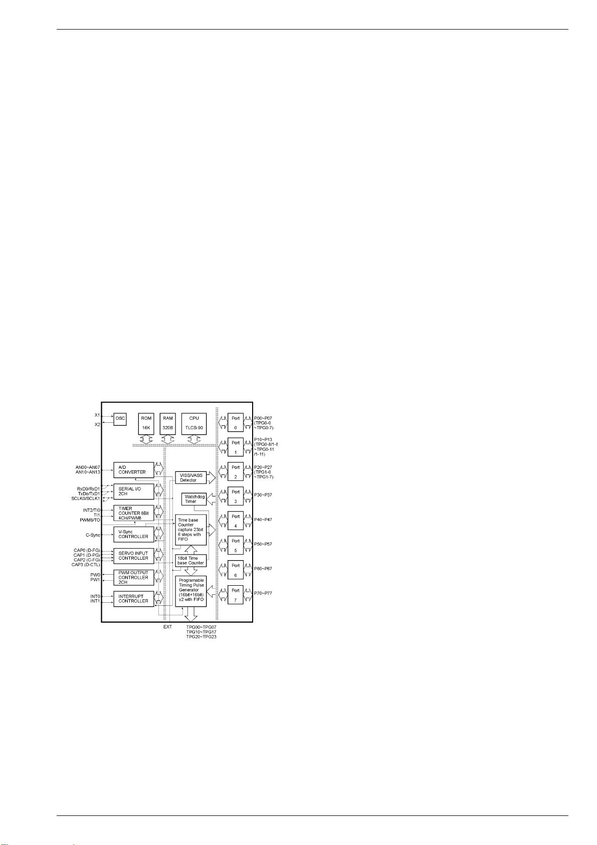
TVR 3710 …, TVR 5100 …,TVR 5500 … Beschreibung
Leuchtfleckunterdrückung und Entladen der Bildröhre
Beim Abschalten des Gerätes ist bei den Zeilentrafos 5550 ohne
Entladewiderstand (Bleeder-Widerstand) die Bildröhre separat zu
entladen und das Nachleuchten des Bildschirms zu unterbinden.
Dabei wird die Emitterschaltung T7902 nicht mehr mit der gleichgerichteten Heizspannung angesteuert. Die folgende Transistorstufe
T7901 wird leitend und zieht die Referenzspannung der RGBVerstärkerstufe nach Masse. Dadurch wird die Bildröhre voll ausgesteuert und entladen. Da keine Fokusspannung mehr anliegt, erscheint am Bildschirm nur ein diffuser Leuchtfleck.
Bei den Zeilentrafos 5551 mit eingebautem Entladewiderstand übernimmt dieser den Abbau der Ladung in der Bildröhre. Damit der
Bildschirm beim Abschalten sofort dunkel ist, wird das Gitter 1 der
Bildröhre zusätzlich gesperrt. Dazu wird im Betrieb C2911 auf +180V
geladen. Beim Abschalten des Gerätes sperrt T7902 und T7903 wird
leitend. Dadurch wird der Plus-Pol des C2911 über T7903 nach Masse
geschaltet und das Gitter 1 der Bildröhre wird mit umgekehrter Polarität angesteuert.
3. Signal-Chassis (PSSP2)
3.1 Signal-Chassis – Laufwerksteuerung /
Deck-Elektronik (DE)
Funktionsübersicht
Die Steuerung des Laufwerks übernimmt der Laufwerksrechner IC7410,
TVC (Toshiba Video Controller) mit dem Mikrocomputer IC7801 auf
der Bedieneinheit. Der Datenaustausch zwischen den Mikrocomputern erfolgt über die bidirektionale serielle Schnittstelle DATD1 / DATD2 /
CLKD1.
Der Laufwerksrechner ist ein speziell für Videorecorder entwickelter
Mikrocomputer. Das Betriebssystem im integrierten maskenprogrammierten ROM des µCs wird durch den Geräteoptionscode im
EEPROM definiert (siehe Servicetestprogramm – Geräte-Optionscode). Die Rechnergeschwindigkeit legt der Quarz Q1400 fest.
TMP91C642
Der Laufwerksrechner übernimmt die Steuerung und die Kontrolle des
Laufwerks inklusive der Servosysteme für den Bandvorschub und die
Kopfscheibensteuerung. Des weiteren steuert dieser die Aufnahme-/
Wiedergabeumschaltung, sowie die Freigabe der Aufsprechströme.
Die Laufwerksteuerung ist in folgende Funktionsgruppen unterteilt:
3.1.1 Reset
3.1.2 Steuerung des Fädelmotors
(Cassettenschacht / Fädelmechanik)
3.1.3 Wickeltachoimpulsverarbeitung
3.1.4 Bandanfang-/ Bandende-Erkennung
3.1.5 Kopfservoregelung
3.1.6 Bandservoregelung
3.1.7 Trackingregelung / Autotracking
3.1.1 Reset
Den Einschaltreset, nach dem Anstecken des Gerätes ans Netz,
erzeugt IC7411 mit dem Resetkondensator C2454 an Pin 4. Der
daraus generierte "POR" (Power On Reset) an IC7411-(17) steht als
HIGH-Impuls (ca. 30ms) über T7405 einmalig am Laufwerksrechner
IC7410-(46) "IPOR" an. Des weiteren gelangt dieser "POR"-Impuls
über die phasendrehende Verzögerungsstufe T7805 auf der Bedieneinheit als negierter Impuls zum Bedienrechner IC7801-(47).
3.1.2 Steuerung des Fädelmotors (Cassettenschacht / Fädelmechanik)
Der Antrieb der Cassettenschacht- und Fädelmechanik erfolgt über
den Fädelmotor. Zur Ansteuerung des Fädelmotors gibt der Laufwerksrechner IC7410 die Steuersignale TMO (Pin 53) und THIO (Pin 16)
aus. Mit diesen steuert man über den Fädelmotor-Treiber IC7402-(5/6,
7/8) und Steckerkontakte 1903-(1/3) den Fädelmotor.
Die Laufwerksposition erkennt der µC durch das Zählen der Fädeltachoimpulse (FTA) in Verbindung mit dem Schalter INIT sowie der Kennung
des "TAS" Bandanfangs sowie des "TAE" Bandendes. Die Fädeltachoimpulse (FTA) werden dem µC über Steckerkontakt 1905-(11) und
IC7411-(5/15) zugeführt (FTAD). Das Laufwerk enthält je einen Schalter
zur Initialisierung des Fädeltachos (INIT) und zur Löschsicherung
(RECP). Die Spannungen entsprechend der Schaltzustände verkoppelt
man über die Steckerkontakte 1905-(14/10), R3471 (INIT) sowie R3472
(RECP) und führt diese dem IC7410-(56) zu.
Der Cassettenschacht ist im angehobenen Zustand mechanisch mit
dem Fädeltachogeber (Flügelrad) verbunden. Beim Einschieben einer
Cassette in den Cassettenschacht muß diese soweit eingeschoben
werden, bis drei Fädeltachoimpulse erzeugt wurden. Danach aktiviert
der Laufwerksrechner den Fädelmotor und übernimmt somit das
Laden der Cassette.
Beim Auswurf (Eject) der Cassette wird kurz vor Erreichen der Endposition des Cassettenschachtes der Empfänger für Bandanfangkennung
mechanisch freigegeben. Kurze Zeit später schaltet der Ablaufrechner
den Fädelmotor ab.
3.1.3 Wickeltachoimpulsverarbeitung
Die Optokoppler am linken und rechten Wickelteller (WTL / WTR)
geben pro Umdrehung des Wickels 8 Impulse ab. Diese werden im
IC7411 (Pins 7/6 –> Pins 13/14) in Rechteckimpulse umgeformt und
über die Pins 15 (WTLD) und 14 (WTRD) dem IC7410 zugeführt.
Dieser errechnet aus dem Verhältnis der beiden Frequenzen den
augenblicklichen Bandstand und die Gesamtlänge der Cassette.
3.1.4 Bandanfang-/ Bandende-Erkennung
Zur Erkennung von Bandanfang und Bandende hat die VHS-Cassette
an den beiden Bandenden eine Klarsichtfolie von 13 bis 19cm Länge.
Über 2 Optokoppler wird Bandanfang und Bandende erkannt. Die über
T7490 getaktete Sendediode taucht dabei in der Cassettenmitte in ein
Loch ein. Die Empfänger sind links und rechts außerhalb der Cassette
angeordnet.
Die Phototransistoren "TAS" (Bandanfang) oder "TAE" (Bandende)
liefern Impulse, wenn sie Bandanfang oder -ende erkennen. Die
Ausgangsspannungen der Phototransistoren werden über die Steckerkontakte 1905-(15/7) den Analogeingängen des µCs IC7410-(55/57)
zugeführt.
3.1.5 Kopfservoregelung
Die Kopfservoregelung sorgt für die richtige Drehzahl und Phase des
Kopfscheibenantriebs. Die gesamte Regelung erfolgt dabei im µC
(IC7410). Die Istwerte werden im Kopfscheibenmotor-Treiber (IC7301)
auf der Kopfverstärkerplatte von den Informationen des Hallgenerators bzw. der Positionsspule im Kopfscheibenmotor (Dreiphasenmotor) in Verbindung mit den Phasenspannungen abgeleitet. Am
Ausgang IC7301-(6) stehen sowohl die PG-Impulse (Phasengenerator)
von 25Hz für die Phasenregelung als auch die FG-Impulse (Frequenzgenerator) von 450Hz für die Drehzahlregelung. Über die Steckverbindung 1904-(1) gelangen die PG-/FG-Impulse zum Laufwerksrechner IC7410-(18).
An IC7410-(30) gibt der µC ein impulsbreitenmoduliertes Rechtecksignal (REEL) aus, das sowohl Drehzahl- als auch Phaseninformationen
enthält. Dieses wird über Steckerkontakt 1904-(6) dem Kopfscheibenmotortreiber IC7301 auf der Kopfverstärkerplatte als Regelspannung
zugeführt.
3.1.6 Bandservoregelung
Der Capstanmotor ist ein Dreiphasenmotor, der mit Hallgeneratoren
bestückt ist. Diese erzeugen Signale, die dem Capstanmotor-TreiberIC (LB1897) auf der Capstanmotor-Einheit über die Pins 8…13 zugeführt werden. Abhängig von diesen Signalen erfolgt in diesem die
Kommutierung der einzelnen Phasen des Capstanmotors.
GRUNDIG Service 2 - 3
j
Page 21

Beschreibung TVR 3710 …, TVR 5100 …,TVR 5500 …
Die Drehrichtungsumschaltung (CREV) erfolgt über den Pin 26 des
LB1897. Dazu gibt der µC (IC7410) an Pin 44 für die Drehrichtung
vorwärts LOW-Pegel bzw. rückwärts HIGH-Pegel aus. Dieses Steuersignal wird über Steckerkontakt 1905-(4) dem Capstanmotor-Treiber
zugeführt. Für die Drehzahlregelung gibt das FG-Hallelement (Magneto
Recitive Element) des Capstanmotors Impulse mit einer Frequenz von
1514Hz bei Nenndrehzahl ab. Die Impulse (FG) vom CapstanmotorTreiber-IC (LB1897) Pin 3 für die Drehzahlregelung werden über
Steckerkontakt 1905-(2), IC7411-(8), dem internen Komparator und
IC7411-(11) dem IC7410-(19) zugeführt. Die Tachoimpulse (Istwert)
werden im IC7410 mit einem intern erzeugten Sollwert verglichen.
Über IC7410-(31) gibt der µC eine impulsbreitenmodulierte Rechteckspannung (CAP) aus. Diese wird mit R3476 / C2471 integriert und
über Steckerkontakt 1905-(3) als Regelspannung dem CapstanmotorTreiber-IC (LB1897) zugeführt.
Bei den Funktionen "Spulen" und "Bildsuchlauf" (≥3) wird die
Versorgungsspannung des Capstanmotor-Treibers von +8,8V auf
+14,6V umgeschaltet. Dies erfolgt über das Steuersignal (IWIND) vom
Laufwerksrechner IC7410-(51) und die Transistorstufe T7493 / T7492 /
T7491.
3.1.7 Trackingregelung / Autotracking
Während der Aufnahme werden über den Synchronkopf codierte
25Hz-CTL-Impulse auf das Band aufgezeichnet, die bei Wiedergabe
zur Spurnachführung benötigt werden.
Diese 25Hz-Impulse gelangen bei Aufnahme von IC7410-(22) zum
IC7411-(16) und von hier über IC7411-(2) und die Steckverbindung
1901-(7) an den Synchronkopf.
Bei Wiedergabe werden die aufgesprochenen CTL-Impulse vom
Synchronkopf abgetastet, im IC7411 in Rechteckimpulse umgeformt
und über IC7411-(16) dem IC7410-(17/20) zugeführt.
Nach dem Einlegen einer Cassette wird bei Wiedergabe mit Hilfe der
Autotracking-Funktion die optimale Spurlage ermittelt. Zu diesem
Zweck führt man dem Hauptrechner IC7410 über den Analogeingang
(Pin 59) eine von der Hüllkurve der FM-Pakete abgeleitete Spannung
"TRIV" (Trackinginformation Video) zu. Diese wird im Kopfverstärker
erzeugt.
Ausgehend von der Tracking-Mittellage wird der Tracking-Sollwert
vergrößert und verkleinert. Für jede der beiden Richtungen wird nun
der zugehörige Sollwert ermittelt, bei dem die von der FM-Hüllkurve
"TRIV" abgeleitete Spannung gegenüber dem maximal ermittelten
Spannungswert abzunehmen beginnt. Als optimaler Trackingwert
wird der Mittelwert zwischen den beiden Eckwerten eingestellt. Nach
Abschluß dieser Messung wird die Autotracking-Funktion abgeschaltet und die ermittelte Phasenlage über die CTL-Impulse geregelt.
Fehlen mehr als zwei aufeinanderfolgende CTL-Impulse, wird das
Autotracking erneut gestartet. Es wird in diesem Fall davon ausgegangen, daß eine neue Aufnahme mit anderer Trackinglage vorliegt.
3.2 Signal-Chassis – Bedieneinheit (CO)
Der Mikrocomputer IC7801 ist das Kernstück der Bedieneinheit und
erfüllt folgende Aufgaben mit den entsprechenden Funktionsgruppen:
– Auswertung der Tastaturmatrix.
– Decodierung der Fernbedienbefehle vom Infrarot-Empfänger
IC7812.
– Quarz-Uhr
– Integriertes RAM zum Speichern der Timer-Daten.
– Leuchtdiodenansteuerung (Timer / Aufnahme / Standby) über
die Pins 28 / 29 / 31
– Bidirektionale serielle Schnittstelle (DATD1 - Pin 7, DATD2 - Pin 8
und CLKD1 - Pin 9) zum Datenaustausch zwischen Bedienrechner
und Laufwerksrechner.
– Über den I2C-Bus (SDA - Pin 56, SCL - Pin 55) sind folgende
Funktionsgruppen miteinander verbunden:
EEPROM – IC7813
Tuner 1 – 1701 oder 1702
Tuner 2 – 1301
VPS/PDC – IC7840
Teletext – IC7881 oder IC7880 (Teletext / VPS / PDC)
– Analog-Ausgänge zur Steuerung folgender Einstellungen über die
Pins:
Pin 18 (VOL) – Lautstärke
Pin 14 (BRI) – Helligkeit
Pin 17 (CONTR) – Kontrast
Pin 15 (SHP/COIN) – Bildschärfe
Pin 19 (SAT) – Farbsättigung
Pin 16 (HUE) – Farbton (TINT für NTSC)
– Die Farbnormumschaltung (optional) erfolgt für Tuner 1 über
folgende Pins:
Pin 5 (PSS) – PAL / SECAM
Pin 11 (MES) – MESECAM / SECAM-L
Pin 63 (SB1_1) – SECAM-L - Band I / III / UHF
Für Tuner 2 (optional) erfolgt die Umschaltung über:
Pin 3 (PSS2) – PAL / SECAM
Pin 6 (MNT2) – MESECAM / SECAM-L
Pin 54 (SB1_2) – SECAM-L - Band I / III / UHF
– Für die Hochspannungsüberwachung erhält der Bedienrechner
über Pin 53 die Kontrollspannung "PROT". Bei einem Fehler im
Hochspannungsteil ist die Spannung <1,5V und die Hochspannungserzeugung wird über die Schaltspannung "MONI" an
Pin 61 abgeschaltet (LOW),
– Bei OSD-Einblendungen gibt der Bedienrechner die Austast-
signale (Pin 33 - ROT, Pin 34 - GRÜN, Pin 35 - BLAU und Pin 36 BLANKING) aus. Der Oszillatorkreis für den internen Spaltenzähler
ist zwischen den Pins 42 und 43. Zur Synchronisation, damit die
richtigen Pixel an der richtigen Position des Bildschirms angezeigt
werden, erhält der Zeichengenerator im Bedienrechner die Horizontal- und Vertikal-Synchronsignale über die Pins 37 und 38. Diese
generiert man mit den Komparatoren im IC7870 aus den "SuperSandcastle"-Impulsen (HFB/SC).
– Das Driften des Tuners 1701 / 1702 oder des Antennensignales
erzeugt im Empfangsschaltungsteil der TV-Signalelektronik die
Regelspannung AFC1. Diese gelangt an Pin 24 und der Bedien-
rechner regelt die Tuner-Abstimmspannung über den I2C-Bus nach.
– Bei einem Netzausfall versorgt der Kondensator C2802 an Pin 64
die Uhr und das RAM mit Spannung. Die Diode D6801 verhindert,
daß sich der Kondensator entlädt. Während dem Netzausfall ist an
Pin 48 LOW-Pegel, so daß weitere Funktionen des ICs mit dem
Systemquarz Q1801 an Pins 45 / 46 abgeschaltet werden.
– Im EEPROM (IC7813) speichert der Bedienrechner (IC7801)
kunden- und gerätespezifische Daten (z.B. Optionscode, Sendereinstellungen-Kanäle, Software-Abgleichwerte). Die Datenübertragung erfolgt über den I2C-Bus (SDA / SCL).
– VPS/PDC-Programmabfrage
Der Bedienrechner schaltet bei mehr als einer vorprogrammierten
VPS-Sendung in einen Abfrage-Modus. Dazu stimmt er in einem
bestimmten Zyklus den Tuner kurzzeitig auf die entsprechenden
Sender ab. Der IC7840 liest die aktuellen VPS-Daten aus und
überträgt sie über den I2C-Bus zum Bedienrechner. Damit ist
gewährleistet, daß der Rechner auch von den Sendeanstalten
vorgezogene Beiträge erkennt und den Videorecorder entsprechend steuert.
3.3 Signal-Chassis – TV-Signalelektronik (TV)
Die TV-Signalelektronik besteht im wesentlichen aus folgenden
Funktionseinheiten, die zum größten Teil im IC7200 integriert sind:
– Empfangseinheit
– Bildsignalverarbeitung
– Tonsignalverarbeitung
– Horizontal- und Vertikal-Synchronisation
3.3.1 Empfangseinheit
Die Empfangseinheit hat die Aufgabe, das vom Tuner kommende ZFSignal zu verstärken und zu demodulieren. Es entstehen dabei das
FBAS-Signal und das Audio-Signal.
Vom Kontakt 17 des Tuners 1701 oder 1702 kommend durchläuft das
ZF-Signal das Oberflächenwellenfilter F1720, das die ZF-Durchlaßkurve bestimmt. Über IC7200-(45/46) führt man es einem regelbaren
Breitbandverstärker mit Synchrondemodulator und danach einem
Videoverstärker zu. Des weiteren erzeugt man in diesem IC die
Regelspannung für den Breitbandverstärker und den Tuner. Diese
Regelspannung gelangt über IC7200-(47) zum Tuner (Kontakt 5). Ihr
Regeleinsatz ist mit R3712 (AGC1) einstellbar. Das demodulierte ZFSignal koppelt man an Pin 7 des IC7200 aus. Nach der Verstärkerstufe
T7762 teilt sich der Signalweg.
– Für die Bildsignalverarbeitung führt man das demodulierte
ZF-Signal über den Ton-Trap 1740, wo man den Tonanteil im
FBAS-Signal absenkt. Dies ist bei den Normen SECAM DK und L
nicht erforderlich. Der Ton-Trap 1740 wird in diesem Fall mit
IC7705-(3…5 / 9) überbrückt. Anschließend gelangt es über den
Impedanzwandler T7216 und IC7200-(13) zum Eingangswahlschalter der Bildsignalverarbeitung (Luminance Switch). Zusätzlich wird es dem "IN/OUT"-Schaltungsteil über T7215 als
"VFV1"-Signal zugeführt.
2 - 4 GRUNDIG Service
j
Page 22

TVR 3710 …, TVR 5100 …,TVR 5500 … Beschreibung
– Das demodulierte ZF-Signal leitet man für die FM-Audiosignal-
verarbeitung über das ZF-Filter F1745 bzw. optional F1746 und
IC7705-(11…14) zum IC7200-(5). Anschließend durchläuft die herausgefilterte Ton-ZF den Begrenzer, den PLL-Demodulator und
gelangt zur Vorverstärker Mute-Schaltung. Danach führt man das
demodulierte Ton-Signal "AFV1" über IC7200-(1) und der
Verstärkerstufe T7703 zum "IN/OUT"-Schaltungsteil.
Bei der AM-Audiosignalverarbeitung (SECAM-L) führt man das ZFSignal vom Kontakt 17 des Tuners 1701 oder 1702 zum Oberflächenwellenfilter 1750. Dieses enthält einen zusätzlichen Eingang entsprechend der im Band I der Empfangsnorm SECAM-L getauschten Bildund Tonträger. Die Eingänge, Pin 1 (Band I) oder Pin 2, des
Oberflächenwellenfilters 1750 werden mit der Schaltspannung "SB1_1"
über T7707 / T7708 freigegeben. Diese führt LOW-Pegel im Band I
der Norm SECAM-L. Das gefilterte ZF-Signal gelangt anschließend
zum IC7754-(1/16). Im IC7754 durchläuft es einen regelbaren Verstärker und einen AM-Demodulator. Danach führt man es über IC7754-(7)
dem Ton-Normumschalter zu. An Pin 8 wird das Audiosignal "AFV1"
ausgekoppelt und dem "IN/OUT"-Schaltungsteil zugeführt.
3.3.2 Bildsignalverarbeitung
Dem Eingangswahlschalter der Bildsignalverarbeitung (Luminance
Switch) wird zum einen das FBAS-Signal der Empfangseinheit an
IC7200-(13) zugeführt und zum anderen über IC7200-(15) das externe FBAS-Signal "VEXT", z.B. des Video-Teils. Danach teilt sich der
Signalverlauf in der "Trap and Bypass"-Stufe in einen für die Luminanzsignalverarbeitung und einen für die Chrominanzsignalverarbeitung.
– Die "Trap"-Stufe filtert aus dem FBAS-Signal den Luminanz-Anteil
(BAS) heraus. Die folgende Verzögerungsleitung (Y-Delay/
Peaking) kompensiert Laufzeitunterschiede zwischen Luminanz-
und Chrominanzsignal. Die "Peaking"-Stufe verbessert die Kanten-
schärfe. Anschließend gelangt das BAS-Signal zur "Luminance/
Matrix"-Stufe, wo die R- / G- / B-Signale gebildet werden.
– Das Chrominanzsignal wird in der "Chrominance-Bandpaß"-Stufe
herausgefiltert. Im Regelkreis (ACC Amplifier) wird die Amplitude
des Chrominanzsignals für die Farbbegrenzung und Farbregelung
kontrolliert und dem PAL-Farbdemodulator zugeführt. Für die Farb-
Demodulation filtert man im Phasendetektor den Burst aus dem
Chrominanzsignal zur Synchronisierung des "XTal"-Oszillators. Die
Frequenz 4,433664MHz legt der Quarz Q1200 an Pin 35 fest. Mit
Hilfe dieser Farbträgerfrequenz werden nun die Farbkomponenten-
signale demoduliert und verlassen als R-Y (Pin 30) und B-Y (Pin 31)
den IC7200. Die SECAM-Demodulation (optional) erfolgt extern im
IC7202. Dazu führt man das Chrominanzsignal über IC7200-(27)
dem IC7202-(16) zu. Die Farbträgerfrequenz erhält der IC7202-(1)
über IC7200-(32) vom "XTal"-Oszillator. Die demodulierten R-Y-
und B-Y-Signale werden an IC7202-(10/9) ausgegeben. Nach der
Verzögerungsleitung IC7201 werden beide Signale (R-Y / B-Y) in
den IC7200-(29/28) eingespeist und geklemmt. Zusätzlich ist in der
Klemmstufe die Farbsättigung mit der Steuerspannung "SAT" an
IC7200-(26) einstellbar. In den folgenden "Matrix"-Stufen bildet man
mit Hilfe des Luminanzsignales die R- / G- / B-Signale.
Die gewonnenen R- / G- / B-Signale durchlaufen den RGB-Wahlschalter (Clamp Switch) und in der Ausgangsstufe (Output Stages) ist
die Helligkeit (BRI) über Pin 17 und der Kontrast (CONTR) über Pin 25
einstellbar. Zusätzlich wird der Kontrast automatisch bei hohen Strahlströmen über Pin 25, D6200 und der "BCI"-Spannung reduziert.
Anschließend verlassen die R- / G- / B-Signale den IC7200-(20/19/18)
und gelangen über den Stecker 1913 zur Bildrohrplatte.
3.3.3 Tonsignalverarbeitung
Das im "IN/OUT"-Schaltungsteil selektierte Audio-Signal (ATV) gelangt direkt zur Audio-Endstufe IC7240-(3). Dieser arbeitet als Brückenverstärker und beinhaltet einen thermischen Überlastschutz. Die Lautstärke ist mit der "VOL"-Steuerspannung an IC7240-(5) einstellbar.
Bei einer kleineren Steuerspannung als 0,4V mutet der IC7240 automatisch.
3.3.4 Horizontal- und Vertikal-Synchronisation
Das im Eingangswahlschalter der Bildsignalverarbeitung (Luminance
Switch) selektierte FBAS-Signal gelangt über die "Trap and Bypass"Stufe zum Amplitudensieb (H AND V SEP.). Dort werden die Horizontal- und Vertikal-Synchronimpulse separiert. Die HorizontalSynchronimpulse gelangen zur "Phase 1"-Regelung und die Vertikal-Synchronimpulse starten den Zeilenzähler (Vertikal Divider) für
die Vertikalsynchronisation.
Mit der "Phase 1"-Regelung wird die Frequenz des internen Horizontaloszillators (Line Oscillator) geregelt. Die Regelzeitkonstande bestimmen die an IC7200-(40) angeschlossenen Bauteile. Die folgende
"Phase 2"-Regelung stellt den Bezug zwischen der tatsächlichen
Position des Elektronenstrahls und dem Zeilensynchronimpuls her.
Dafür werden die Zeilenrückschlagimpulse dem IC7200-(38) zugeführt und ausgewertet. Die dabei resultierende Regelspannung wird
mit C2204 an IC7200-(39) geglättet. Die horizontale Position des
Bildes ist ebenfalls über Pin 39 durch einen Gleichspannungsoffset
mit dem Einsteller R3206 (H-SHIFT) festgelegt. Die Horizontalimpulse
(HDR) gelangen über IC7200-(37) und Steckerkontakt 1911-(2) zur
Horizontalendstufe auf dem Leistungs-Chassis.
Der Zeilenzähler (Vertikal Divider) gibt bei 312 Zeilen den Bildsynchron-Impuls ab. Dieser triggert den Sägezahngenerator der "Vertikal
Output"-Stufe des IC7200, der auf dem Prinzip einer Konstantstromquelle funktioniert. Hierfür ist der Kondensator C2200 an IC7200-(42)
angeschlossen. Für diverse Einstellungen (Bildlinearität, Bildhöhe
und vertikale Lage) erhält die "Vertikal Output"-Stufe des IC7200 von
der Vertikal-Endstufe (Leistungs-Chassis) über IC7200-(41) das "VFB"Signal als Rückkopplung. Die Einstellregler sind auf dem LeistungsChassis und beeinflussen das Rückkoppel-Signal "VFB". Der geregelte Ablenksägezahn "VDR" verläßt den IC7200 an Pin 43 und gelangt
über den Steckerkontakt 1922-(5) zur Vertikalendstufe auf dem
Leistungs-Chassis.
3.4 Signal-Chassis – Empfangseinheit 2 (TU2)
Die Empfangseinheit 2 hat die Aufgabe, bei Geräten mit 2 Tunern
(einer für TV, der andere für Video) für die Videoaufzeichnung das vom
Tuner kommende ZF-Signal zu verstärken und zu demodulieren. Es
entstehen dabei das FBAS-Signal und das Audio-Signal.
Signalverarbeitung bei Bestückung des IC7300
Vom Kontakt 17 des Tuners 1301 kommend durchläuft das ZF-Signal
das Oberflächenwellenfilter F1320, das die ZF-Durchlaßkurve bestimmt. Über IC7300-(1/2) führt man es einem regelbaren Breitbandverstärker mit Synchrondemodulator und danach einem Videoverstärker zu. Des weiteren erzeugt man in diesem IC die Regelspannung für den Breitbandverstärker und den Tuner. Diese Regelspannung
gelangt über IC7300-(12) zum Tuner (Kontakt 5). Ihr Regeleinsatz ist
mit R3341 (AGC2) einstellbar. Das demodulierte ZF-Signal durchläuft
zwischen Pin 13 und Pin 14 des IC7300 einen Ton-Trap F1340, wo
man den Tonanteil im FBAS-Signal absenkt. Anschließend wird es
verstärkt und über IC7300-(7) sowie der Verstärkerstufe T7310 dem
"IN/OUT"-Schaltungsteil (als "VFV2"-Signal) zugeführt.
Das demodulierte ZF-Signal für die FM-Tonverarbeitung wird über
IC7300-(13) ausgekoppelt. Über das ZF-Filter F1345 und IC7300-(11)
führt man es der FM-Demodulation zu. An IC7300-(9) steht das NFSignal "AFV2", das nach dem Deemphasisglied R3324 / C2319 und
der Verstärkerstufe T7309 über den "IN/OUT"-Schaltungsteil dem
Ton-Schaltungsteil zugeführt wird.
Signalverarbeitung bei Bestückung des IC7301
Im IC7301 werden das Videosignal und das Audiosignal getrennt von
einander aufbereitet und demoduliert.
– Video-Signalverarbeitung
Vom Kontakt 17 des Tuners 1301 kommend durchläuft das ZFSignal das Oberflächenwellenfilter F1320, das die ZF-Durchlaßkurve bestimmt. Über IC7301-(1/2) führt man es einem regelbaren
Breitbandverstärker mit Synchrondemodulator und danach einem
Videoverstärker zu. Des weiteren erzeugt man in diesem IC die
Regelspannung für den Breitbandverstärker und den Tuner. Diese
Regelspannung gelangt über IC7301-(16) zum Tuner (Kontakt 5).
Ihr Regeleinsatz ist mit R3341 (AGC2) einstellbar. Das demodulierte ZF-Signal durchläuft zwischen Pin 18 und Pin 19 des IC7301
einen Ton-Trap F1340, wo man den Tonanteil im FBAS-Signal
absenkt. Dies ist bei den Normen SECAM-DK und SECAM-L nicht
erforderlich. Der Ton-Trap 1340 wird in diesem Fall mit
IC7312-(11…14) überbrückt. Anschließend wird es verstärkt und
über IC7301-(8) sowie der Verstärkerstufe T7310 dem "IN/OUT"Schaltungsteil (als "VFV2"-Signal) zugeführt.
– Audio-Signalverarbeitung
Vom Kontakt 17 des Tuners 1301 kommend durchläuft das ZFSignal das Oberflächenwellenfilter F1322, das die ZF-Durchlaßkurve bestimmt. Über IC7301-(27/28) führt man es einem regelbaren
Breitbandverstärker mit Synchrondemodulator zu. Das demodulierte ZF-Signal gelangt zum einen über den AM-Demodulator direkt
zum Ausgangsverstärker. Zum anderen wird es für die FM-Demodulation über IC7301-(17) ausgekoppelt. Nach dem ZF-Filter F1345
oder F1346, dem Wahlschalter IC7312-(1/2/10/15) und
IC7301-(15) führt man es über den FM-Demodulator (FM-PLL) dem
Ausgangsverstärker zu. Anschließend gelangt es als "AFV2"-Signal
über IC7301-(10) zum "IN/OUT"-Schaltungsteil.
GRUNDIG Service 2 - 5
j
Page 23

Beschreibung TVR 3710 …, TVR 5100 …,TVR 5500 …
3.5 Signal-Chassis – IN/OUT (IO)
Allgemeines
Die universelle Einsatzmöglichkeit der Geräte erfordert eine spezielle
Verteilung der Eingangs- und Ausgangs-Signale, entsprechend der
Betriebsart. Dazu sind die Schalter-ICs IC7591, IC7592 und IC7593
nötig.
3.5.1 Eingangs- / Ausgangswahlschalter
Die Selektion und Verteilung der Signale erfolgt in Schalt-ICs. In den
einzelnen Geräten sind je jach Ausführung folgende Wahlschalter
eingesetzt:
– IC7591 Eingangswahlschalter (optional) für die TV-Signal-
elektronik. Am TV-Eingangswahlschalter stehen die Bild- und Audiosignale des Tuners 1, der Buchse EURO-AV, der Buchsen
Cinch-AV (für Camcorder) und der Schaltungsteile Video/Chroma
und Standardton.
– IC7592 Eingangswahlschalter für den Video/Chroma-Schaltungs-
teil
Am Video-Eingangswahlschalter stehen die Bild- und Audiosignale
des Tuners 1 oder 2, der Buchse EURO-AV und der Buchsen CinchAV (für Camcorder).
– IC7593 Ausgangswahlschalter für die Buchse EURO-AV (optional)
Am EURO-AV-Ausgangswahlschalter stehen die Bild- und Audiosignale des Tuners 1, des Tuners 2 und des TV-Eingangswahl-
schalters bzw. des Video-Teils.
Diese werden entsprechend der Betriebsart ausgewählt und den
Schaltungsteilen für Video/Chroma "VR", Standardton "AMLR" TVSignalverarbeitung "VTV" / "ATV" und der Buchse EURO-AV zugeführt.
Die Steuerung übernimmt der Laufwerksrechner IC7410 über die
Steuerleitungen VS1 / VS2 für IC7591, RS1 / RS2 für IC7592 und
OS1 / OS2 für IC7593.
3.3.2 Decoder-Betrieb
Aus urheberrechtlichen und finanztechnischen Gründen verschlüsseln einige private Fernsehanstalten die Bild- und Tonsignale. Zum
Entschlüsseln dieser Signale benötigt der Empfänger einen entsprechenden PAY-TV-Decoder.
Technische Ausführung
An der Buchse EURO-AV ist der PAY-TV-Decoder anzuschließen.
Bei der Benutzung des PAY-TV-Decoders leitet man die codierten
Bild- und Audiosignale über die Buchse EURO-AV zum PAY-TVDecoder. In diesem werden die Signale decodiert und über die Buchse
EURO-AV dem "IN/OUT"-Schaltungsteil wieder zugeführt. Dieser
Signalweg muß beim Einstellen der Programme programmbezogen
freigegeben sein.
Dieser Signalweg wird im TV-Betrieb über die Schalt-ICs (IC7593 /
IC7591) freigegeben. Beim Video-Betrieb erfolgt die Freigabe über die
Schalt-ICs (IC7593 / IC7592).
3.6 Signal-Chassis – Video/Chroma (VS)
Durchschleif-Signalweg (EE)
Das im "IN/OUT"-Schaltungsteil ausgewählte FBAS-Signal (VR) gelangt zum Pin 12 des IC7051. In diesem durchläuft es die VIDEO-AGCStufe, einen R/P-Schalter und verläßt nach dem Video-Verstärker
(VIDEO AMP) den IC7051 an Pin 16. Danach leitet man das FBASSignal (VP) zum "IN/OUT"-Schaltungsteil.
nahme unwirksam sind und verläßt nach dem R/P-Schalter den
IC7051 an Pin 4. An der Basis der folgenden Verstärkerstufe T7007 ist
ein 4,43MHz-Sperrkreis, der den Chromaanteil im FBAS-Signal unterdrückt. Das herausgefilterte BAS-Signal leitet man über einen Emitterfolger (T7007) und C2027 zum IC7051-(5). In diesem durchläuft es
eine Klemmstufe, einen DETAIL ENHANCER und die NLE-Stufe
(nichtlineare Anhebung).
Bei der Betriebsart SP ist der DETAIL ENHANCER und bei LP
zusätzlich die NLE-Stufe wirksam. Die Aktivierung (LOW-aktiv) der
NLE-Stufe erfolgt über IC7051-(25). In der folgenden linearen Preemphasis (MAIN EMPH) hebt man die hochfrequenten Anteile des BASSignals linear an. Diese Anhebung wird bei Wiedergabe rückgängig
gemacht. Man erreicht dadurch einen besseren Signal-/Rauschabstand. Die äußere Beschaltung für das nichtlineare Netzwerk besteht
aus C2024 und R3012 (an Pin 8), die für das lineare Netzwerk aus
R3014, C2025, C2026, C2062 und R3013 (an Pin 7). Über IC7051-(7)
stellt man an der MAIN EMPH-Stufe den Synchronwert (R3010) des
Luminanz-Signales ein. Der Weißwert ist nicht veränderbar. Das
Luminanz-Signal führt man intern im IC7051 zum FM-Modulator.
Das frequenzmodulierte Signal verläßt an Pin 2 den IC7051 und
gelangt über ein Tiefpaßfilter (T7010) zum Knotenpunkt R3023 /
R3029 / R3027. An diesem wird es mit dem Chroma-Signal addiert.
Das Summenprodukt (FMRV) führt man über die Verstärkerstufe
T7018 / T7019 und Steckerkontakt 1902-(2) dem Kopfverstärker zu.
Wiedergabe
Bei Wiedergabe gelangt das Signal vom Band (FMPV) über Steckerkontakt 1902-(9) zu einigen Anpaßstufen, für Frequenzgang und
Laufzeit (C2043…T7014). Anschließend führt man es über den Emitterfolger T7013 zum Pin 1 des IC7051.
Im IC7051 teilt sich der Signalweg. Zum einen gelangt das Signal vom
Band für die Dropout-Erkennung zum Dropout-Detektor (DO DET),
der bei einem Pegeleinbruch mit definierter Größe einen Impuls an die
Drop–Out-Kompensations-Schalter (DO) abgibt. Zum anderen führt
man es über eine Begrenzerstufe (DOUBLE LIM), einen FM-Demodulator, ein Tiefpaßfilter (SUB LPF), eine Deemphasis-Stufe (MAIN
DEEMPH) mit Wiedergabe-Amplitudeneinstellung und einen R/PSchalter zum Pin 4 des IC7051. Danach gelangt das BAS-Signal über
eine Verstärkerstufe (T7007) und C2027 zum IC7051-(5). Das Signal
wird im IC7051 vor und nach dem R/P-Schalter geklemmt (CLAMP).
Nach dem folgenden Tiefpaßfilter (Y-LPF) teilt sich der Signalweg.
Zum einen durchläuft das Luminanz-Signal einen Dropout-Schalter
und verläßt nach einem R/P-Schalter den IC7051 am Pin 20. In der
folgenden Verzögerungsschaltung (IC7060) wird es um eine Zeile
verzögert und über IC7051-(18) und die folgende Verstärkerstufe
(VCA) dem Dropout-Schalter zugeführt. Treten dropoutbehaftete Signale auf, werden diese durch Umschalten des Dropout-Schalters
durch das einwandfreie, verzögerte Signal ersetzt. Zum anderen wird
das unverzögerte und das verzögerte BAS-Signal in einem Differenzverstärker subtrahiert und die dabei entstehende, niederfrequente
Rauschspannung über ein Bewertungsfilter mit dem unverzögerten YSignal gegenphasig addiert. Das rauschverminderte Y-Signal durchläuft die nichtlineare Deemphasis (NL DEEMPHASIS), die Rauschunterdrückung (WHI NOI CAN) für hochfrequente Rauschspannungen
und eine Stufe zur Höhenanhebung (PICTURE CONTROL). In der
nachfolgenden "Y/C-MIX"-Stufe wird das Y-Signal mit dem intern
zugeführten Chromasignal addiert. Das zurückgewonnene FBASSignal durchläuft einen R/P-Schalter, die V-Impulseintastung (QH/QV
INS, CHARA INS), einen Video-Verstärker (VIDEO AMP) und verläßt
an Pin 16 den IC7051. Danach leitet man das FBAS-Signal (VP) zum
"IN/OUT"-Schaltungsteil.
3.6.1 Signal-Chassis – Video
Funktionsübersicht
Bei Aufnahme bereitet das Videoschaltungsteil das FBAS-Signal auf
und setzt das Luminanz-Signal in ein frequenzmoduliertes Signal um.
Bei Wiedergabe durchläuft das vom Band abgetastete, frequenzmodulierte Signal den Demodulator, einen Dropout-Kompensator, eine
Entzerrerstufe und die Bildschärfestufe. Anschließend wird das BASSignal mit dem Farbsignal addiert und dem "IN/OUT"-Schaltungsteil
zugeführt.
Aufnahme-Signalweg
Das im "IN/OUT"-Schaltungsteil ausgewählte FBAS-Signal (VR) gelangt im IC7051 vom Pin 12 zur Video-AGC-Stufe, durchläuft anschließend einen -6dB-Abschwächer (1/2), einen R/P-Schalter, eine Klemmstufe (CLAMP), ein Tiefpaßfilter (Y-LPF), einige Stufen, die bei Auf-
2 - 6 GRUNDIG Service
j
3.6.2 Signal-Chassis – Chroma "PAL/SECAM-BG"
Funktionsübersicht
Bei Aufnahme wird das 4,43MHz-F-Signal mit Hilfe einer Mischfrequenz (5,06MHz) auf 627kHz umgesetzt.
Bei Wiedergabe wird aus dem 627kHz-F-Signal mit Hilfe der Mischfrequenz (5,06MHz) das ursprüngliche 4,43MHz-F-Signal wiedererstellt.
Es wird verstärkt, zum Luminanz-Signal addiert und dem "IN/OUT"Schaltungsteil zugeführt.
Aufnahme
Der Signalweg ist bei Aufnahme für PAL und MESECAM (Secam Ost)
gleich. Das FBAS-Signal (VR) vom "IN/OUT"-Schaltungsteil wird über
Pin 12 dem IC7051 zugeführt. In diesem IC durchläuft es die VideoAGC-Stufe, einen -6dB-Abschwächer (1/2), einen R/P-Schalter und
einen integrierten Bandpaß (FSC BPF). Hier wird das Chroma-Signal
vom FBAS-Signal herausgefiltert. Anschließend gelangt das Chroma-
Page 24

TVR 3710 …, TVR 5100 …,TVR 5500 … Beschreibung
Signal über zwei R/P-Schalter, einen Regelverstärker (ACC AMP) und
eine Burst-Emphasisstufe (unwirksam) zum Hauptmischer (MAIN
CONV). Im Hauptmischer werden das Chromasignal (4,43MHz) und
die anstehende Hilfsträgerfrequenz (5,06MHz) gemischt. Das umgesetzte Chromasignal (627kHz) wird im internen Tiefpaß von unerwünschten Mischprodukten befreit. Nach dem folgenden R/P-Schalter, dem Chroma-Tiefpaßfilter (C-LPF) und dem Farbkiller gelangt es
zum Pin 38 des IC7051. Danach führt man es über den Einsteller für
den Chroma-Aufsprechstrom, R3029 (PAL CURR.), zum Knotenpunkt R3023 / R3029. An diesem wird es mit dem Y-Signal addiert.
Das Summenprodukt (FMRV) führt man über die Verstärkerstufe
T7018 / T7019 und Steckerkontakt 1902-(2) dem Kopfverstärker zu.
Wiedergabe
Über den Steckerkontakt 1902-(9) erreicht das Signal vom Band
(FMPV) den IC7051-(38) im Chromaschaltungsteil. Von hier läuft es
über zwei R/P-Schalter zum Chroma-Tiefpaßfilter, wo das 627kHzChroma-Signal selektiert wird. Anschließend durchläuft das 627kHzChroma-Signal einen 6dB-Verstärker, einen geregelten Verstärker
(ACC AMP) und gelangt über eine Burst-Emphasis-Stufe (unwirksam)
zum Hauptmischer (MAIN CONV). Hier wird es mit der Hilfsträgerfrequenz (5,06MHz) gemischt. Das zurückgewonnene Chromasignal
(4,43MHz) gelangt danach über einen R/P-Schalter zum integrierten
Chroma-Bandpaß (FSC BPF). Danach kommt es zum einen direkt
über IC7051-(24) und IC7060-(2) zum Kammfilter im IC7060. Zum
anderen wird es zusätzlich für PAL/NTSC invertiert und über den
MESECAM-Schalter, IC7051-(23) und IC7060-(4) an das Kammfilter
im IC7060 weitergeleitet.
Die Funktion des Kammfilters besteht darin, das invertierte Signal von
IC7060-(4) bei PAL um 2 Zeilen (bei NTSC um eine Zeile) zu
verzögern und es mit dem direkten Signal von IC7060-(2) kommend zu
addieren. Diese beiden Signalwege zusammen bilden das "Kammfilter" zur Übersprechkompensation. Beim MESECAM-Betrieb wird
dem Kammfilter nur das direkte Signal zugeführt. Dadurch kann das
Kammfilter nichts mehr addieren und ist somit ohne Funktion. An
Pin 23 gibt das Kammfilter IC7060 das Chromasignal aus und führt es
über Pin 26 dem IC7051 zu. In diesem durchläuft es einen MESECAMWahlschalter, ein Tiefpaßfilter (LPF), einen R/P-Schalter und eine
Verstärkerstufe mit Farbkiller. Nach dem Chroma-Bandpaßfilter (FSC
BPF), IC7051-(29/28) und der Chroma-Rauschunterdrückung (CHROMA N.C.) wird es in der "Y/C-MIX"-Stufe zu dem intern zugeführten
Luminanzsignal addiert. Der weitere Signalverlauf entspricht dem des
Luminanzsignales.
Trägeraufbereitung (PAL/NTSC)
– Aufnahme (PAL)
Zur Trägeraufbereitung verwendet man einen spannungsgesteuerten
Quarzoszillator (VXO) im IC7051, dessen Oszillatorfrequenz
(4,433619MHz) von dem an den Pins 32 und 31 angeschlossenen
Quarz (Q1000) bestimmt wird. Der REC-APC-Detektor vergleicht die
Phase des ankommenden Senderbursts mit der des VXO und regelt
diesen nach. Die an IC7051-(33) stehende Regelspannung wird mit
C2008, R3001 und C2009 geglättet. Des weiteren verwendet man
einen im IC7051 integrierten Oszillator (321FH VCO). Dieser wird von
der Synchronfrequenz geregelt. Der VCO schwingt auf einem Vielfachen der Zeilenfrequenz (321fH). Das entspricht einer Frequenz von
5,015625MHz. In einem 4-Phasenschieber teilt man diese Frequenz
durch 8 und führt sie dem Hilfsmischer (SUB CONV) zu. Hier wird sie
mit der Oszillatorfrequenz des VXO (4,433619MHz) gemischt. Dabei
entsteht der Hilfsträger von 5,06MHz. Dieser durchläuft einen internen
5,06MHz-Bandpaß (SUB BPF) und wird anschließend dem Hauptmischer (MAIN CONV) zugeführt.
– Wiedergabe (NTSC/PAL)
Bei Wiedergabe verwendet man den frei auf der Quarzfrequenz
(Q1000 – 4,433619MHz) schwingenden XO-Quarzoszillator als Referenz und den VCO-Oszillator. Der VCO wird jetzt, nach erfolgter
Rückmischung des Chromasignals von 627kHz (PAL) bzw. 629kHz
(NTSC) auf 4,43MHz-Hilfsträgerfrequenz, vom Burst des wiedergegebenen F-Signals synchronisiert. Die PB-APC-Stufe erzeugt die Regelspannung für den VCO und vergleicht dabei die Phase des Quarzoszillators mit der Phase des rückgemischten 4,43MHz-Bursts. Die
Zeitkonstante des Siebgliedes an IC7051-(37) ergibt sich aus C2003,
R3000 und C2004. Im 4-Phasenschieber teilt man diese Frequenz
durch 8 und führt sie dem Hilfsmischer (SUB CONV) zu. Hier wird sie
mit der Oszillatorfrequenz des XO gemischt. Dabei entsteht unter
anderem der Hilfsträger von 5,06MHz. Dieser wird über das interne
Bandfilter (SUB BPF) dem Hauptmischer (MAIN CONV) zugeführt.
3.6.3 Signal Chassis – Chroma "SECAM L"
Aufnahme
Das FBAS-Signal (VR) vom "IN/OUT"-Schaltungsteil gelangt über den
Emitterfolger T7101 zu der Stufe für die Chromaselektion (Q5103 /
T7100). Danach leitet man das selektierte Chromasignal über die
Trapschaltung (L5102 / C2102 / L5101 / C2101 / R3102) zum
IC7151-(29). Diese Trapschaltung erhöht die Selektionswirkung des
"Glockenkreises" (Q5103). Anschließend durchläuft es einen 15dBVerstärker und wird über die Pins 25 und 24 einem Begrenzerverstärker mit nachfolgendem Frequenzteiler zugeführt. Dieser erzeugt durch
1:4-Teilung des Chroma-Signals das für die Aufnahme benötigte
1,1MHz-Signal, das zum Pin 21 des IC7151 durchgeschaltet wird.
Dieses gelangt nach dem folgenden Bandpass, in dem die bei der
Frequenzteilung entstandenen Oberwellen abgesenkt werden, zum
Pin 19 des IC7151. Danach durchläuft es einen 10dB-Verstärker und
wird zum Pin 15 durchgeschaltet. Zwischen den Pins 15 und 14 führt
man das 1,1MHz-Signal über den "Antiglockenkreis" (Q5108). Im
IC7151 wird es begrenzt und gelangt über Pin 17 zum Einsteller für den
SECAM-Chroma-Aufsprechstrom, R3027 (SECAM-CURR.), zum Knotenpunkt R3027 / R3023. An diesem wird es mit dem Y-Signal addiert.
Das Summenprodukt (FMRV) führt man über die Verstärkerstufe
T7018 / T7019 und Steckerkontakt 1902-(2) dem Kopfverstärker zu.
Steuerung der Umschalter im IC7151
Bei Aufnahme liegt LOW-Pegel (0,7V) am Kollektor des Transistors
T7105. Dieser wirkt wie eine Diode, wird leitend und legt ca. 1,3V an
IC7151-(23). Die nachfolgende Detektionsstufe erkennt dadurch Aufnahmebetrieb und schaltet alle IC-internen Schalter in Stellung Aufnahme.
Wiedergabe
Bei Wiedergabe wird das "ungeregelte FM-Signal vom Band" (FMPV)
zum Pin 23 des IC7151 geleitet und anschließend um 6dB verstärkt.
Von Pin 21 aus leitet man es über einen Bandpaß zum IC7151-(19).
Das gewonnene 1,1MHz-Signal durchläuft zwischen den Pins 19 und
18 einen 10dB-Verstärker und wird über Pin 16 einem weiteren
Verstärker im IC7151 zugeführt, dessen Rückkopplungszweig einen
"Antiglockenkreis" (Q5108) enthält. Dieser ist zwischen den Pins 14
und 15 angeschlossen. In der dem Verstärker folgenden AGC-Stufe
wird das Signal ausgeregelt und dessen Frequenz in der Zweiweggleichrichterstufe "RECTIFIER f x2" verdoppelt (2,2MHz). Über IC7151-(10)
leitet man das 2,2MHz-Signal dem Bandpass R3126…R3127 zu, der
das Nutzsignal von störenden Oberwellen befreit. In einer weiteren
Verdopplerstufe, der das 2,2MHz-Signal über IC7151-(8) zugeführt
wird, bildet man das 4,4MHz-Signal. Anschließend wird es um 10dB
verstärkt und gelangt über Pin 31, den Antiglockenkreis (Q5100) und
Pin 32 zum Colour-Killer. Von IC7151-(1) leitet man das 4,4MHzSignal dem Bandpass (R3122…C2121) zu, der das Nutzsignal von
störenden Oberwellen befreit. Das gewonnene SECAM-Chroma-Signal gelangt über den Impedanzwandler T7106 zum IC7051-(28) und
wird dort zum BAS-Signal addiert.
3.7 Signal-Chassis – Standardton (AL)
Funktionsübersicht
Die bei Aufnahme dem Standardton-Schaltungsteil zugeführten NFSignale gelangen zum Aufnahmeeingang des IC7601 und werden
anschließend für die Längsspuraufzeichnung aufbereitet.
Bei Wiedergabe wird das NF-Signal vom AW-Kopf abgenommen, verstärkt
und der TV-Signalelektronik sowie der Buchse EURO-AV zugeführt.
3.7.1 Aufnahme
Das im "IN/OUT"-Schaltungsteil ausgewählte NF-Signal (AMLR) gelangt über IC7601-(11) und eine Aussteuerungsautomatik (ALC-Automatic Level Control) an einen linearen Verstärker (AMP). Das Signal
erreicht über IC7601-(13), C2611, R3612, R3613 sowie IC7601-(14)
den integrierten Aufnahme-Entzerrerverstärker (AMP). An Pin 17
verläßt es den IC7601. Das NF-Signal wird am Knotenpunkt R3617 /
R3618 zum Aufsprechstrom addiert und anschließend über Steckerkontakt 1901-(1) dem AW-Kopf zugeführt. Das andere Ende des AWKopfes liegt über 1901-(3), R3600 und IC7601-(2) an Masse. Die
Vormagnetisierungs-Spannung ist mit R3618 (BIAS) einstellbar.
Für die Funktion "LP" wird die Umschaltung der Aufnahme-Entzerrung
mit dem Schalter EP CTL im IC7601 durchgeführt.
GRUNDIG Service 2 - 7
j
Page 25
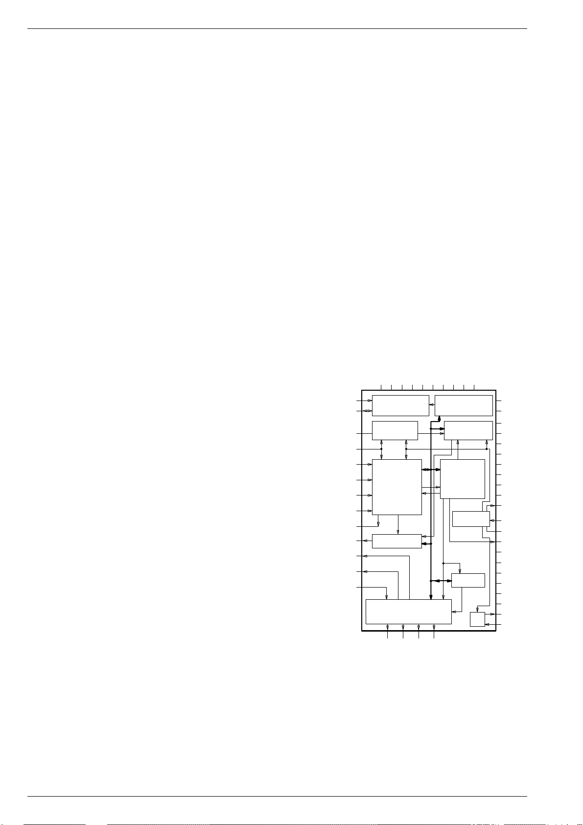
Beschreibung TVR 3710 …, TVR 5100 …,TVR 5500 …
3.7.2 Löschoszillator
Der selbstschwingende Oszillator für den Haupt- und Tonlöschkopf
besteht aus dem Transistor T7603 und dem Resonanzkreis F5603 /
C2622. Von diesem wird auch die Vormagnetisierungsspannung
(BIAS) abgeleitet. Die Ansteuerung des Oszillators erfolgt über den
Aufnahme-Schaltpegel "IREC" (aktiv bei LOW) vom Laufwerksrechner
IC7410-(9) und die folgenden Transistoren T7606 / T7605 / T7604.
3.7.3 Wiedergabe
Bei Wiedergabe erhält der AW-Kopf über IC7601-(1) und Steckerkontakt 1901-(1) Massepotential. Das vom AW-Kopf abgetastete NF-Signal
gelangt über 1901-(3) an IC7601-(2). Es durchläuft im IC7601 den
integrierten Wiedergabeentzerrer (EQ), wird über IC7601-(8) und den
Pegeleinsteller für Wiedergabe R3606 (PB-LEVEL) dem IC7601-(9)
zugeführt. Anschließend wird es in einem linearen Verstärker (AMP)
verstärkt. An Pin 13 verläßt das NF-Signal den IC7601. Nach der
Verstärkerschaltung IC7608 mit Zeilenfrequenz-Sperrfilter wird das
Signal (AMLP) über den "IN/OUT"-Schaltungsteil der TV-Signalelektronik
bzw. der Buchse EURO-AV zugeführt.
Bei "LP"-Wiedergabe bewirkt der Schalter EP CTL die EntzerrungsUmschaltung.
3.7.4 Stummschaltung
Der Mute-Befehl (MTA) vom Laufwerksrechner IC7410-(40) dient dazu,
die Tonausgänge des IC7601 bei allen Funktionen, außer Wiedergabe
und Aufnahme, sowie bei Servofehlern stummzuschalten. Dazu erhält
der IC7601 über Pin 22 den Mute-Befehl "MTA" (aktiv bei HIGH).
4. Teletext "DOS" (TXT)
Funktionsübersicht
Der Teletext-Schaltungsteil enthält einen Testbild-/Datengenerator
und die VPS-/PDC-/Teletextverarbeitung. Das Kernstück ist der IC7881
oder IC7880 (mit VPS- und PDC-Verarbeitung). Diese Beschreibung
bezieht sich auf den IC7880. Dieser IC7880, IVT (Integrated VideoInput-Processor and Teletext), beinhaltet folgende Funktionsgruppen:
– Datenabtrennung
Die adaptive Datenabtrennstufe gewinnt aus dem über IC7880-(8)
zugeführten FBAS-Signal (VTV) die VPS-/PDC-/Teletextdaten. Zu
diesem Zweck gelangt das Videosignal auf einen A/D-Wandler. Auf
digitaler Basis erfolgt anschließend die Abtrennung der Daten und
die Aufbereitung des zugehörigen Taktes (6,9375MHz für PDC/
Teletext und 2,5MHz für VPS). Der Schwarzwert des FBAS-Signals
wird mit C2888 an IC7880-(7) gespeichert. Der Referenzstrom für
die analoge Signalverarbeitung wird über IC7880-(9) abgeleitet.
– Takt-PLL
Die freilaufende 27MHz-Oszillatorfrequenz wird mit dem Quarz
Q1800 an IC7880-(2…4) festgelegt und zunächst für den A/D-
Wandler verwendet. Zum anderen erzeugt daraus eine digital arbei-
tende PLL die Grundfrequenzen 6MHz, 1MHz und 15,625kHz. Die so
erzeugte Zeilenfrequenz wird dann, ebenso wie die aus dem FBAS-
Signal abgetrennten Zeilensynchronsignale, einem Phasenvergleich
zugeführt. Die Charakteristik des nachgeschalteten digitalen Schlei-
fenfilters wird durch ein Steuerregister beeinflußt und der 6MHz-
Oszillator entsprechend nachgeregelt. Auf diese Weise sind alle vom
IVT generierten Frequenzen mit dem FBAS-Signal zeilenverkoppelt.
Im Freilauf (z.B. Testbild) ist der Phasenvergleich abgeschaltet.
–I2C-Bus-Interface
Über dieses Interface können alle Abläufe vom Hauptrechner
(IC7880) gesteuert und jede Stelle im Seitenspeicher beschrieben
oder gelesen werden.
– Steuerlogik
Die Steuerlogik besteht aus mehreren Zählern, Gatterverknüpfungen
und Steuerregistern, die über den I2C-Bus ansteuerbar sind. Diese
wird mit den intern erzeugten 6MHz-, 1MHz-, H- und V-frequenten
Impulsen versorgt. Auf diese Weise entstehen unter anderem das
Sync.-Signal (IC7880-(12)), der Pixel-Takt für den Zeichengenerator,
sowie die Steuersignale für das Seitenspeicher-Interface.
– Datenakquisition
In den Zeilen 16 für VPS, 2…22 und 315…335 für PDC/Teletext
liefert die Steuerlogik ein sog. Dateneingangsfenster. Der
Akquisitionskreis erkennt entsprechende Daten anhand eines festgelegten Rahmencodes. Anschließend erfolgt eine Seriell-/Parallelwandlung und eine Fehlererkennung bzw. Fehlerkorrektur. Fordert
der Benutzer eine Textseite an, wird über den I2C-Bus ein Register
mit der Seitennummer geladen. Die Akquisition vergleicht nun alle
ankommenden Seitennummern mit der angeforderten Seite und
leitet deren Abspeicherung im Seitenspeicher ein.
– Seitenspeicher
In dem 8k x 8-DRAM sind bis zu 8 Teletextseiten sowie die PDCund VPS-Daten speicherbar.
– Zeichengenerator
Man unterscheidet 256 Zeichen. Jedem dieser Zeichen ist ein 8BitDatenwort zugeordnet. 32 davon sind Steuerzeichen, der Rest ist
graphisch bzw. alphanumerisch in Form einer Rasterpunktmatrix
aus 12 horizontalen und 10 vertikalen Punkten zusammengesetzt.
Abgelegt sind diese Zeichen im Character-ROM des IVT. Der
zeilenverkoppelte 1MHz-Takt schaltet die Adressen am
Seitenspeicher weiter. Der das jeweilige Zeichen repräsentierende
8Bit-Code wiederum bildet einen Teil der Adresse am CharacterROM. Der andere Teil wird durch einen Zeilenzähler gebildet. Am
Ausgang des ROM entsteht so nach jeweils 1µs ein der Helligkeitsinformation entsprechendes 12Bit-Datenwort. Dieses wird in ein
Schieberegister geladen und mit einem vom 6MHz-Takt abgeleiteten 12MHz-Pixeltakt ausgelesen. Die entsprechenden R-/G-/BSignale stehen an den Push-Pull-Ausgängen IC7880-(15…17) zur
Verfügung. Den maximalen Ausgangspegel der R-/G-/B-Signale
legt die Spannung am IC7880-(18) fest. Das Blank-Signal von
IC7880-(19) verwendet man zur Steuerung der R-/G-/B-Eintastung
im IC7200 der TV-Signalelektronik (Signal-Chassis).
IC7880
SAA5281
23
24
11
13
12
21
20
22
18
26 27 28 29 30 31 32 33 34 35
Clamp
AD-Conversion
8
7
Sync separation
and processing
9
Digital PLL
ODD/EVEN OR DV
Character Generator Buffers
Character ROM
15 16 17
19
Control RegistersI2C Businterface
Data slicing
and Acquisition
Acquisition
and Display
Line Counters
Oscillator
8k Memory
10
1
4
56
14
25
48
47
46
45
2
3
4
44
43
42
41
40
39
38
37
/2
36
2 - 8 GRUNDIG Service
j
Page 26
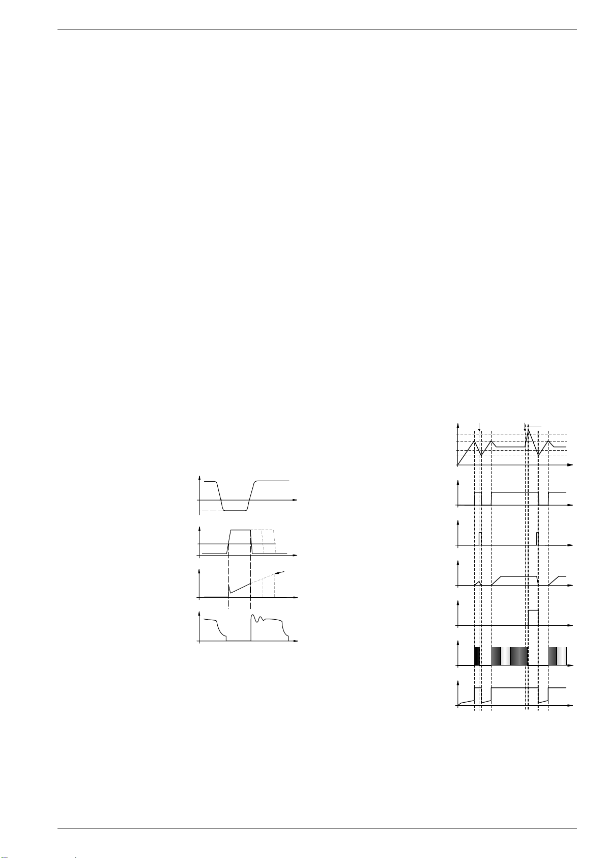
IC7310-(1)
IC7310 int.
IC7310 int.
IC7310-(11)
IC7310 int.
IC7310-(3)
IC7310-(1)
V
cc
V
cc prot
V
cc start
V
ref
V
dis2
V
dis1
V
pin11
UVLO1
V
ovp out
Output
I
cc
17mA
0,3mA
No-Take Over
Re-Start
Start-Up
Normal Mode
Loop Failure
>2ms
t
t
t
t
t
t
t
TVR 3710 …, TVR 5100 …,TVR 5500 … Descriptions
current flows through the secondary windings of the transformer,
Description
k
through the diodes, electrolytic capacitors into the load.
When the whole amount of energy stored in the transformer has been
transferred to the load and no magnetic field is left in the transformer,
1. Power Chassis (PLSP)
1.1 Power Chassis – Power Supply
Typical Data:
Mains voltage: 196…265V~
Mains frequency: 45…65Hz
Maximum power: 130W
Switching frequency: 30…85kHz
Efficiency: 80% at maximum load
Short-circuit protection provided for all outputs
Principle of the Blocking-Oscillator Type Transformer
During the conducting phase of the switching transistor T7330 energy
is transferred from the mains to the transformer. This energy is fed out
to the load during the phase the transistor is switched off. By means of
the switch-on period and the frequency the energy transfer during each
cycle is so controlled that the output voltages are independent of
changes in the load or the input voltage. Controlling and driving the
switching transistor is effected by IC7310.
The Different Load Conditions
– No-load operation (STANDBY / TIMER record programming):
From the power consumption the IC7310 recognizes no-load condition and reduces the frequency to 30kHz to minimize the switching
losses at the Power-MOS transistor T7330.
– Normal operation (control range):
The switching frequency decreases along with the increasing load.
The duty cycle is mainly controlled by the mains voltage. The output
voltages are influenced by the load to a minor extent.
– Reversal point:
At this point of the output characteristic the maximum power is
transferred.
– Overload:
The power supply operates in Burst Mode (polling operation mode),
i.e. the energy of each cycle is limited so that the output power is low.
Circuit Description
The mains voltage is rectified by the bridge rectifier D6313…D6316
and filtered by C2315. L5311 is provided to protect the power supply
against interfering pulses from the mains. During the starting phase the
power for IC7310 is supplied to
Pin 1 via R3331 and C2310.
After the starting phase the
power is obtained from the
transformer winding 4 / 3 and
D6334. The inductance of the
primary windings 1 / 5…7 determines the natural frequency
of the switched mode power
supply in normal operating
mode. The maximum frequency
is determined by C2327 at
IC7310-(10).
During the switch-on period of
the switching transistor T7330
the current of the rectified mains
voltage flows through the primary winding of the transformer
(contacts 1 / 5…7), T7330 and
R3334, R3335 to ground (in the primary side). Since the voltage at
contact 1 of the transformer is almost constant the current rises
linearly. The intensity of this current depends on the mains voltage and
the inductance of the primary winding. In the transformer, a magnetic
field develops which corresponds to a certain amount of energy.
During this phase, the diodes are cut off due to the polarity of the
secondary voltages. Via the resistors R3334, R3335, R3359 a voltage
which represents the primary current is fed to Pin 7 of IC7310. If this
voltage exceeds a certain level depending on the control voltage at
IC7310-(14), the switching transistor T7330 is switched off. This
process is repeated whenever the switching transistor T7330 is
switched on.
As soon as the switching transistor T7330 is switched off the energy
transfer to the transformer is stopped. The energy accumulated in the
transformer is now transferred to the secondary windings. Due to the
fact that the polarities of the voltages are reversed by the transformer
GRUNDIG Service 2 - 9
+U
IC7310-(8)
U
IC7310-(3)
T7330
U
T7330
-U
GS
Dmax
I
D
DS
I
Point of Reversal
the voltages at the secondary windings fall below 0V. These zero
passages are detected by IC7310 at Pin 8. The transistor T7330 is
switched on again and the next cycle is started.
Control of the switched mode power supply is effected by varying the
conducting phase of the switching transistor to the effect that the
energy transferred from the mains to the transformer is increased or
reduced. The control information is obtained from the transformer
winding 3 / 4 and is taken via D6335 / C2337 and R3356…R3358 to
Pin 14 of IC7310. The amplifier "ERROR AMP" IC7310 compares this
voltage with an internal 2.5V reference voltage. By means of this
comparison the level of the voltage used to be compared with the
voltage at Pin 7 of IC7310 (representing the primary current) is
changed.
During the period T7330 is switched off, C2332 / D6332 and C2331 /
R3345 limit the voltage peaks in the primary side.
To avoid static charges the gate of the switching transistor T7330 is
provided with the pull-down resistor R3339. The voltage at Pin 5 of
IC7310 is used for stepping down the current and the voltage in shortcircuit conditions (FOLD BACK).
The maximum power possible to be taken from the secondary side is
determined by R3334 / R3335. At 1V (typically) on IC7310-(7) the
power supply unit reaches the reversal point.
The external circuit at Pin 11 is an option of IC7310. By means of
C2320 the pulses in the start-up phase are shorter so that the switching
frequency is outside the audible range.
From the secondary side, eleven voltages (Ubat, 33A, 14H, 14/9M1,
14M1, 14M2, 9A, 5D1, 5D, 5A and -7V) are available which are rectified
and filtered by the respective components (diodes / capacitors / chokes).
In Standby mode, the 5D1, 5D, and 5A voltages are switched off by the
"STBY" switching voltage via T7351 / T7532.
The Start-up Phase
When connecting the video recorder to the mains the following
voltages at the pins of IC7310 start to rise at time t0 (see fig.):
– The voltage Vcc,
IC7310-(1), increases
according to the halfwave charge via R3331
until it reaches the voltage level Vcc Start at the
typical current consumption (Icc) of 0.3mA.
t
The internal reference
voltage Vref of IC7310
is switched on as soon
as Vcc Start is reached
and the current consumption increases to
t
17mA.
– The voltage at Pin 11 of
IC7310 rises linearly up
to 2.4V. During this pe-
t
riod, IC7310 drives the
Power-MOS transistor
T7330 by shortened
pulses.
– If the voltage Vcc,
t
IC7310-(1), falls below
the limit value Vdis2 before the reversal point is
reached the start-up is
stopped. For this, the
drive to T7330 is
stopped and IC7310
switches off the internal
Vref (Icc = 0.3mA). The
voltage Vcc increases according to a half-wave charge via R3331.
The next start-up cycle commences.
Normal Operation, Overload and Standby Operation
As soon as the power supply stage is working, IC7310 operates in the
normal mode (control range). The voltage at IC7310-(14) is 2.5V
(typically). If the load in the secondary side increases, the switch-on
period of T7330 is increased. As a result the peak voltage value at
IC7310-(7) "representation of drain current" increases.
k
Page 27

Descriptions TVR 3710 …, TVR 5100 …,TVR 5500 …
If the load continues to increase, that is also the voltage at IC7310-(7),
the overload amplifier of the IC starts to reduce the pulse width of the
T7330 driving voltage at IC7310-(3). This point is the so-called reversal
point. The IC supply voltage Vcc behaves in the same way as do the
secondary voltages. This voltage decreases also along with the
increasing load.
With Vcc < Vdis1, the IC7310 changes to the polling operation mode
(Burst Mode). The short-circuiting power is low because the interval
between the half-wave starts is large. The pulse width is reduced along
with the decreasing load. The switching frequency increases to the
oscillator frequency of IC7310 which is determined at Pin 10 by C2327.
If the load continues to decrease, IC7310 switches the frequency back
to approx. 30kHz (standby operation) from a certain threshold of the
voltage at Pin 7 (depending on the external circuit connected to
Pins 12 / 16). As a result, the switching losses at the transistor are low.
Overvoltage
At an operating voltage Vcc > 17V at Pin 1 of IC7310 the output stage
is switched off.
Excess Temperature
IC7310 is fitted with an excess-temperature sensor for blocking the
logic if the permissible chip temperature is exceeded (typ. 155oC). After
the temperature has fallen a new start-up is possible by re-connecting
the video recorder to the mains.
1.2 Power Chassis – High Voltage Section
The high voltage section is driven by the TV Signal Electronics on the
signal chassis. It contains the TV-IC7200 with the following circuit
stages for generating the drive signals:
– Sync pulse separation
– Horizontal oscillator
– Phase comparison between the horizontal oscillator and the line
flyback pulse
– Vertical oscillator
– Phase comparison between the vertical oscillator and the field
flyback pulse
Horizontal Deflection
The horizontal oscillator within IC7200 feeds out the "HDR" squarewave signal on pin 37 which is then taken via plug contact 1922-(4) to
the horizontal deflection stage. This horizontal deflection consists of
the driver stage (T7587 / T7584 / transformer 5581), the horizontal
output stage (T7583), the horizontal deflection and the line transformer
(5550 or 5551).
The horizontal deflection is made up of the deflection coils, the forward
scan capacitor "S-correction capacitor" (C2584) and the flyback capacitors (C2585 / C2586). Current flows through the diode, integrated
in the line transistor, during the first half of scan (the electron beam
moves from the left edge to the middle of the screen), and the transistor
is switched on during the second half period of scan (from the middle
to the right edge of the screen). During the line flyback period, the line
transistor and the diode integrated in it are not conducting. The forward
scan and flyback capacitors are now in series. The resonant frequency
is increased and consequently the flyback speed as well (typ. t = 12µs).
The horizontal linearity (S-correction) is determined by the forward
scan capacitor C2584 and the linearity coil L5510 (optional). Line
tearing, a typical symptom occuring at the cross-over points in a grid
pattern test picture in high beam current condition, is eliminated by
R3587 / C2587 / D6582. Suppression of the ringing behaviour (antiringing) is achieved by series connection of the line transformer and an
optional resonant circuit (L5590 / C2589 / optionally R3589 or R3590).
The horizontal flyback pulse (HFB/SC), 900V typical amplitude, is fed
for phase comparison through the voltage divider R3597 / R3594 /
R3595, T7585 and plug contact 1922-(5) to the signal chassis - TV
Signal Electronics IC7200-(38).
EHT Generation
When the line transistor T7583 is conducting, the line output transformer 5550 or 5551 is charged up. In this way, the high voltage for the
picture tube during the non-conducting period of T7583 is produced.
The line output transformer is also used to obtain the necessary
voltages for focussing, brightness, cathode heating, the RGB output
stage and the vertical deflection.
Vertical Deflection
The vertical oscillator within IC7200 feeds out at pin 43 the "VDR" sawtooth signal which is taken through plug contact 1922-(1) to the vertical
output stage IC7510-(1/3). The vertical deflection current flows from
2 - 10 GRUNDIG Service
k
the push-pull output stage in IC7510-(5) through the vertical deflection
coils, the coupling capacitor C2519 and the measuring resistors
R3525 / R3559. For attenuating and suppressing the horizontal deflection signals resulting from crosstalk from the horizontal to the vertical
deflection coils, C2516 and R3517 are connected in parallel with the
vertical deflection coils.
The picture height is adjustable with the control R3523 (v-amp.) which
is in parallel with the measuring resistors R3525 / R3559. The signal
(VFB) provided at the wiper is fed via plug contact 1922-(2) as a
negative feedback signal to the signal chassis - TV Signal Electronics
IC7200-(41). Adjustment of the correct vertical position is achieved by
applying a DC current to the vertical deflection coils via the preset
R3524 (v-shift). The picture linearity is determined by the setting of the
preset R3522. For this function, the parabolic voltage at C2519 is
integrated by C2520 / R3522 altering the current into a "S-"shaped
form which is used for correction.
Beam Current Limiting
The voltage drop (BCI) at the low-end capacitor C2551 is used for
determining the average beam current. For this function, the BCI
voltage is fed through plug contact 1923-(3) to the TV Signal Electronics (signal chassis). Together with the diode D6200 located there the
BCI voltage is used to reduce the contrast setting when the beam
current is too high, and to control the vertical picture amplitude.
The Safety Circuit
If the picture tube develops a fault condition the safety circuit
(D6550…D6554 / D6556 / T7550) will be activated. In this case, a
LOW level (<1.5V) is present at plug contact 1923-(2), in normal
operating condition the level is HIGH (>3.5V). This control voltage,
called "PROT", is fed to the µC IC7801-(53) (signal chassis - keyboard
control unit) for evaluation. If the µC identifies a fault condition, the µC
uses the "MONI" status signal to stop the drive to the horizontal output
stage and thus switches the TVR to standby mode. For this purpose,
the "MONI" status signal is at LOW level thus applying via T7206 /
T7205 (TV Signal Electronics) a HIGH level to the horizontal output
stage so that the drive to this stage is stopped.
The safety circuit is triggered in the following operating conditions:
– beam current is too high (>1.5mA)
The average beam current is measured as a voltage drop on C2551.
If the beam current exceeds 1mA, the voltage will be negative going.
Form a level of approx. -18V, the diodes D6550…D6552 conduct
and the voltage at plug contact 1923-(2) decreases to <1.5V.
– EHT is too high
The voltage at the secondary winding 10 / 9 of the line output
transformer 5550 or 5551 rises linearly with the increasing EHT and
is used to trigger the safety circuit. The threshold at which T7550
starts to conduct thus causing the voltage at plug contact 1923-(2)
to decrease to <1.5V is mainly determined by the diodes D6553,
D6556, D6554 and R3554. The triggering threshold for the safety
circuit depends on the screen size:
• 14" typ. 29kV
• 20" / 21" typ. 30.5kV
– failure of the vertical deflection stage
A failure of the vertical deflection stage causes IC7510 to feed out
a HIGH level from pin 7 so that T7550 starts to conduct. Consequently, the voltage at plug contact 1923-(2) rises to levels <1.5V so
activating the safety circuit.
The failure is caused by:
• short circuit or interruption in the vertical deflection coils
• short circuit in the coupling capacitor C2519
• voltage at IC7510-(8) <1V resulting from a defective component
in the vertical deflection.
2. Tube PCB
Drive to the CRT Cathodes
On the picture tube panel the RGB signals (RED / GREEN / BLUE)
coming from the signal chassis are inverted and amplified within
IC7900 (TDA6103Q/N2) to correspond to the CD level of the picture
tube. The gain of the red channel is fixed, the gain of the amplifiers for
the green channel and blue channel is adjusted by the presets R3919 /
R3921. As a result, the output amplitude can be adjusted in respect to
the red output amplitude to yield the desired colour temperature at
white level. The CUT-off presets R3917, R3918 and R3920 are
provided to adjust the DC level of the amplifier output signals making
it possible to compensate for the differences in the cut-off points (start
of beam emission) of the individual picture tube guns.
Page 28
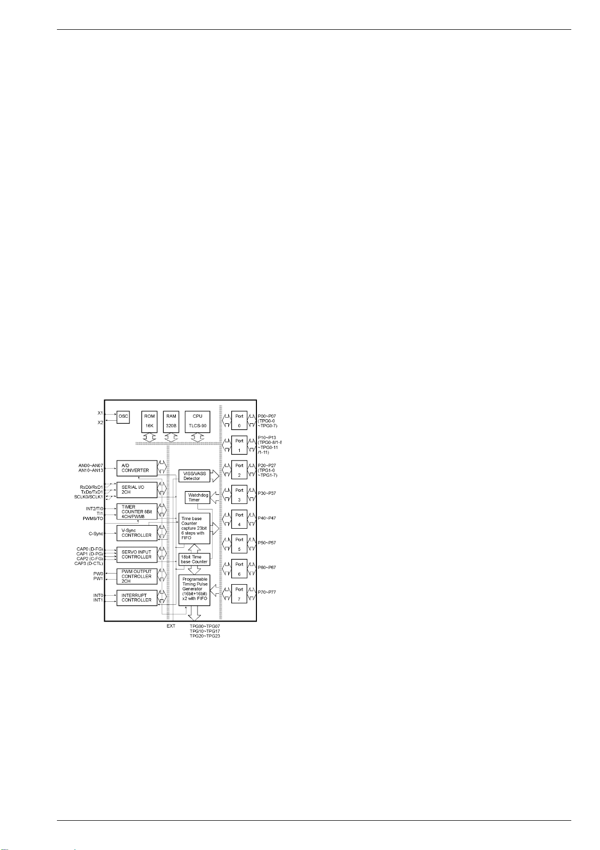
TVR 3710 …, TVR 5100 …,TVR 5500 … Descriptions
Beam Spot Suppression and CRT Discharge
When switching off a TVR the line output transformers 5550 of which
are not provided with a bleeder resistor, the picture tube must be
discharged separately and afterglow of the screen must be prevented.
For this, the rectified heater supply for the emitter stage T7902 is
stopped. The transistor stage T7901 which follows will conduct and
pulls the reference voltage of the RGB amplifier stage to chassis
potential. As a result, the picture tube is fully driven and discharged.
Because there is no focusing voltage, there is only a diffuse spot to be
seen on the screen.
In line output transformers 5551 with integrated bleeder resistor, this
resistor takes over the function of discharging the picture tube. To
ensure that the electron beam is immediately cut off when the TVR is
switched off, grid 1 of the picture tube is also cut off. For this, C2911
is charged up to +180V during operation. When the TVR is switched off,
so does T7902 and T7903 conducts. Consequently, the positive plate
of C2911 receives chassis potential via T7903 and grid 1 of the picture
tube is driven at reverse polarity.
3. Signal Chassis (PSSP2)
3.1 Signal Chassis – Deck Control /
Deck Electronic (DE)
Function Overview
Deck control is effected by the deck computer IC7410, TVC (Toshiba
Video Controller) together with the microcomputer IC7801 on the
keyboard control unit. Data communication between the two microcomputers takes place via the bidirectional serial interface DATD1 /
DATD2 / CLKD1.
The deck computer is a microcomputer especially developed for video
recorders. The operating system stored in the integrated maskprogrammed ROM of the µC is defined by the VCR option code in the
EEPROM (see Service Test Programme - Option Code). The computing speed is determined by quartz Q1400.
TMP91C642
The deck computer is responsible for driving and checking the tape
deck including the servo systems for the tape transport and headwheel
control. It also controls the record/playback switching process and the
release of the recording currents.
The deck control consists of the following function groups:
3.1.1 Reset
3.1.2 Threading Motor Control
(cassette compartment / threading mechanism)
3.1.3 Winding Tachopulse Processing
3.1.4 Beginning of Tape / End of Tape Detection
3.1.5 Head Servo Control
3.1.6 Tape Servo Control
3.1.7 Tracking / Autotracking
3.1.1 Reset
When connecting the video recorder to the mains, the IC7411 generates the switch-on reset pulse with the reset capacitor C2454 on pin 4.
The resulting "POR" (Power On Reset) on IC7411-(17) is applied once
as a HIGH pulse (approx. 30ms) via T7405 to the deck computer
IC7410-(46) "IPOR". On another path, this "POR" pulse is also fed via
the phase-shifting delay circuit T7805 on the keyboard control unit to
the control computer IC7801-(47) as a negated pulse.
3.1.2 Threading Motor Control (cassette compartment /
threading mechanism)
The cassette compartment and threading mechanism is driven by the
threading motor. For driving the threading motor, the deck computer
IC7410 feeds out the control signals TMO (Pin 53) and THIO (Pin 16).
These signals drive the threading motor via the threading motor driver
IC7402-(5/6, 7/8) and plug contact 1903-(1/3).
The µC detects the position of the tape deck by counting the threading
tachopulses (FTA) in connection with the INIT switch and the identification "TAS" for the beginning of the tape, and "TAE" for the end of the
tape. The threading tachopulses (FTA) are supplied to the µC via plug
contact 1905-(11) and IC7411-(5/15) (FTAD). The tape deck is fitted
with a switch for initialisation of the threading tacho (INIT) and another
for erase protection (RECP). The voltages resulting from the switch
settings are coupled via the plug contacts 1905-(14/10), R3471 (INIT)
and R3472 (RECP) and fed to the IC7410-(56).
The cassette compartment is mechanically connected with the threading tacho generator (vane wheel). When loading a cassette into the
cassette compartment, the cassette must be inserted as far as is
necessary to generate three threading tachopulses. Afterwards, the
deck computer activates the threading motor which then takes over the
loading of the cassette.
When ejecting the cassette, the phototransistor detecting the beginning of the tape is released mechanically a short time before the lift
reaches the end position. A short time later, the threading motor is
automatically switched off by the sequence control computer.
3.1.3 Winding Tachopulse Processing
The optocouplers on the left (WTL) and right (WTR) reels produce 8
pulses per revolution. These pulses are formed into rectangular
signals by IC7411 (pins 7/6 –> pins 13/14) and applied to pins 15
(WTLD) and 14 (WTRD) of IC7410. This IC calculates the instantaneous tape position and the total length of the cassette from the ratio of
these two frequencies.
3.1.4 Beginning of Tape / End of Tape Detection
To identify the beginning of tape and end of tape, the VHS cassette has
a clear foil, 13 -19cm long, on each end of the tape. The beginning and
end of tape is identified by two optocouplers. For this purpose, the
transmitting diode which is triggered by T7490 is inserted into a hole
in the middle of the cassette. The phototransistors are located at the
outside, left and right, of the cassette.
The phototransistors "TAS" (beginning of tape) or "TAE" (end of tape)
supply pulses as soon as they detect the beginning or end of tape. The
output voltages of the phototransistors are fed via the plug contacts
1905-(15/7) to the analog inputs of the µC IC7410-(55/57).
3.1.5 Head Servo Control
The head servo control ensures that the rotational speed and the
phase of the headwheel drive are correct. The complete control is
carried out in the µC (IC7410). The actual values are derived in the
headwheel motor driver (IC7301) on the head amplifier board from the
information given by the Hall generator or the position coil located in the
headwheel motor (threephase motor) in connection with the phase
voltages. At the output IC7301-(6) there are the PG (phase generator)
pulses of 25Hz for the phase control and also the FG (frequency
generator) pulses of 450Hz for the speed control. From the connector
1904-(1) the PG/FG pulses are fed to the deck computer IC7410-(18).
On IC7410-(30) the µC feeds out a pulse-width-modulated squarewave signal (REEL) containing information on the speed and the
phase. This signal is fed via the plug contact 1904-(6) to the headwheel
motor driver IC7301 located on the head amplifier board and is used
as a control voltage.
3.1.6 Tape Servo Control
The capstan motor is a three-phase motor which is fitted with Hall
generators. These generate signals which are fed to the capstan motor
driver IC (LB1897) in the capstan motor assembly via the pins 8…13.
Depending upon these signals the IC commutates the individual
phases of the capstan motor.
Switching over of the sense of rotation (CREV) is carried out via pin 26
of the LB1897. For this the µC (IC7410) feeds out from pin 44 a LOW
GRUNDIG Service 2 - 11
k
Page 29

Descriptions TVR 3710 …, TVR 5100 …,TVR 5500 …
level for the forward sense of rotation or a HIGH level for the reverse
direction. This control signal is passed through plug contact 1905-(4)
to the capstan motor driver. For speed control, the FG Hall element
(Magneto Recitive Element) in the capstan motor generates pulses at
a frequency of 1514Hz at the rated speed. The pulses (FG) from the
capstan motor driver IC (LB1897) pin 3 for speed control are fed via
plug contact 1905-(2), IC7411-(8), to the internal comparator and
IC7411-(11) to IC7410-(19). The tachopulses (actual value) are compared in the IC7410 with an internally generated reference value. From
IC7410-(31) the µC feeds out a pulse-width-modulated square wave
voltage (CAP). This is integrated by R3476 / C2471 and fed via plug
contact 1905-(3) as a control voltage to the capstan motor driver IC
(LB1897).
For the functions "Wind/Rewind" and "Picture Search Forward/Backward" (≥3) the supply for the capstan motor driver is switched over from
+8.8V to +14.6V. This is done by the control signal (IWIND) from the
deck computer IC7410-(51) and the transistor stage T7493 / T7492 /
T7491.
3.1.7 Tracking / Autotracking
During recording, encoded 25Hz-CTL-pulses are recorded onto the
tape via the sync head. These pulses are required on playback for
tracking control.
On recording, the 25Hz pulses are taken from IC7410-(22) to
IC7411-(16) and are then passed through IC7411-(2) and the connector 1901-(7) to the sync head.
On playback, the recorded CTL pulses are scanned by the sync head
to be subsequently converted to square wave pulses in IC7411 and
passed on via IC7411-(16) to IC7410-(17/20).
When a cassette is loaded, the Autotracking function determines the
optimum track position on playing back. For this, a voltage "TRIV"
(Tracking Information Video) is derived from the envelope of the FM
packages and fed in to the main computer IC7410 on the analog input
(pin 59). This voltage is generated in the head amplifier.
On the basis of the tracking centre position, the nominal tracking value
is increased or reduced. For each of the two directions, the appropriate
nominal value is determined at which the voltage derived from the FM
envelope "TRIV" starts to decrease as against the maximum determined voltage level. The mid-value between the two limit values is then
used as the optimum tracking value. On completion of this measurement, the Autotracking function is switched off and the determined
phase is controlled by the CTL pulses.
If more than two successive CTL pulses are missing, the Autotracking
function is reactivated assuming, in this case, that a new recording with
a different tracking position is played back.
– Chroma standards switching (optional) for tuner 1 is effected via:
Pin 5 (PSS) – PAL / SECAM
Pin 11 (MES) – MESECAM / SECAM-L
Pin 63 (SB1_1) – SECAM-L - Band I / III / UHF
For tuner 2 (optional) the switching of chroma standards is effected via:
Pin 3 (PSS2) – PAL / SECAM
Pin 6 (MNT2) – MESECAM / SECAM-L
Pin 54 (SB1_2) – SECAM-L - Band I / III / UHF
– For monitoring the EHT, the control voltage "PROT" is applied via
pin 53 to the keyboard control computer. If there is a fault in the EHT
stage, the voltage level is <1.5V and the EHT generation is stopped
by the switching voltage "MONI" on pin 61 (LOW).
– For on-screen-display of information the keyboard control com-
puter feeds out the blanking signals (pin 33 - RED; pin 34 - GREEN;
pin 35 - BLUE, and pin 36 BLANKING). The oscillator circuit for the
internal column counter is located between pin 42 and pin 43. For
synchronising the inserted display, for determining the position of
the appropriate pixels on the screen, the horizontal and vertical
synchronising pulses are fed through pins 37 and 38 to the character
generator within the keyboard control computer. These synchronising pulses are generated from the Super Sandcastle pulses (HFB/
SC) by the comparators in IC7870.
– The drifting of tuner 1 or of the aerial signal produces the AFC1
control voltage in the Frontend circuit of the TV-Signalelectronic.
This voltage is supplied to pin 24 and the keyboard control computer
readjusts the tuner tuning voltage via the I2C bus.
– In the case of power failure the capacitor C2802 provides the
supply for the clock and the RAM at Pin 64. The diode D6801
prevents the capacitor from discharging. During the time of the
power failure, a LOW level exists at Pin 48 so that further functions
of the IC are switched off by the system quartz Q1801 at pins 45 / 46.
– In the EEPROM (IC7813) the control computer (IC7801) stores
special data of the customer and the machine (eg. option code,
station tuning data/channels, software/adjustment values). The
data is transferred via the I2C-bus (SDA / SCL).
– VPS/PDC programme scanning
The keyboard control computer takes up a scanning mode if two and
more VPS transmissions have been preprogrammed. For this, the
computer tunes the tuner at certain intervals and for a short time to
the respective TV stations. The IC7840 reads out the current VPS
data and transfers it on the I2C-bus to the keyboard control computer. It is therefore ensured that the computer detects also transmissions for which the TV stations have fixed an earlier broadcasting
time than originally planned, and that the video recorder is controlled
accordingly.
3.2 Signal Chassis – Keyboard Control Unit (CO)
The microcomputer IC7801 is the heart of the keyboard control unit and
takes over the following functions together with the corresponding
function groups:
– Evaluation of the keyboard matrix.
– Decoding of the remote control commands from the infra-red
receiver IC7812.
– Quartz clock
– Integrated RAM for storing the timer data
– Driving the light emitting diodes (Timer / Record / Standby) via
pins 28 / 29 / 31
– Bidirectional serial interface (DATD1 - pin 7, DATD2 - pin 8 and
CLKD1 - pin 9) for data communication between the keyboard
control computer and the deck computer.
– I2C-bus (SDA - pin 56, SCL - pin 55) connecting the following
function groups with each other:
EEPROM – IC7813
Tuner 1 – 1701 or 1702
Tuner 2 – 1301
VPS/PDC – IC7840
Teletext – IC7881 or IC7880 (Teletext / VPS / PDC)
– Analog outputs controlling the following settings via:
pin 18 (VOL) – volume level
pin 14 (BRI) – brightness
pin 17 (CONTR) – contrast
pin 15 (SHP/COIN) – picture sharpness
pin 19 (SAT) – colour saturation
pin 16 (HUE) – hue (TINT for NTSC)
3.3 Signal Chassis – TV Signal Electronics (TV)
The TV Signal Electronics consists essentially of the following function
groups, most of which are integrated in IC7200:
– Frontend
– Video signal processing
– Audio signal processing
– Horizontal and vertical synchronisation
3.3.1 Frontend
The Frontend has the function of amplifying and demodulating the IF
signal fed in from the tuner. The resulting signals are the CCVS signal
and the audio signal.
Coming from the tuner contact 1701-(17) or 1702-(17), the IF signal
passes through the surface acoustic wave filter F1720, which determines the IF band pass. Via IC7200-(45/46), the signal is fed to a
gain controlled wideband amplifier with synchronous demodulator,
and subsequently, to a video amplifier. Another stage in this IC is used
to generate the control voltage for the wideband amplifier and the
tuner. This control voltage is fed from IC7200-(47) to the tuner
(contact 5). The control threshold level is adjustable with R3712
(AGC1). The demodulated IF signal is fed out from pin 7 of IC7200.
After the amplifier stage T7762 the signal path divides.
– For video signal processing, the demodulated IF signal passes
through the sound trap F1740, in which the audio component of the
CCVS signal is attenuated. For the SECAM DK and L television
standards, the signal does not need to be subjected to the sound trap
1740 which is bridged by IC7705-(3…5 / 9) for this purpose. Subsequently, the signal is fed through the impedance converter T7216
and IC7200-(13) to the input selection switch of the video signal
processing stage (Luminance Switch). Additionally, the signal is
passed to the "IN/OUT" circuit stage via T7215 as the "VFV1"-signal.
2 - 12 GRUNDIG Service
k
Page 30

TVR 3710 …, TVR 5100 …,TVR 5500 … Descriptions
– The demodulated IF signal for FM audio signal processing is fed via
the IF filter F1745, or optionally via F1746 and IC7705-(11…14), to
IC7200-(5). Subsequently, the filtered sound IF is subjected to the
limiter, the PLL demodulator and is passed on to the preamplifier /
mute circuit. The demodulated audio signal "AFV1" passes through
IC7200-(1) and amplifier T7703 to arrive at the IN/OUT circuit stage.
The IF signal for AM audio signal processing (SECAM-L) is fed from
contact 17 of the tuner 1701 or 1702 to the surface acoustic wave filter
F1750. This filter is provided with an additional input for the vision and
sound carriers in Band I of the SECAM-L standard which are reversed
when compared to the other Bands. The inputs, pin 1 (Band I) and pin
2, of the surface acoustic wave filter F1750 are released by the
switching voltage "SB1_1" via T7707 / T7708. This voltage is at LOW
level on Band I of the SECAM-L standard. The filtered IF signal is then
taken to IC7754-(1/16). In IC7754, the signal is passed to a gain
controlled amplifier and an AM demodulator. Subsequently, it is fed
through IC7754-(7) to a sound standards switch. The "AFV1" audio
signal is fed out from pin 8 and taken to the "IN/OUT" circuit stage.
3.3.2 Video Signal Processing
The input selection switch of the video signal processing stage
(Luminance Switch) receives two CCVS signals for selection, the
signal from the frontend at IC7200-(13) and the external signal "VEXT",
e.g. from the VCR stage, at IC7200-(15). Subsequently, the signal path
in the "trap and bypass" stage divides. One path is to the luminance,
the other path to the chrominance processing stage.
– The trap separates the luminance component (CVS) from the CCVS
signal. The integrated delay line (Y-delay/peaking) compensates for
the time differences between the luminance and the chrominance
signal. The peaking stage improves the sharpness of the edges. The
CVS signal is then taken to the luminance/matrix stage where the
R/G/B signals are generated.
– The chrominance signal is filtered by passing it through the chromi-
nance bandpass. The amplitude of the chrominance signal is
controlled in a control circuit (ACC amplifier) for colour limiting and
colour gain and is then fed to the PAL colour demodulator. For colour
demodulation, the burst is sampled from the chrominance signal in
a phase detector. The burst is used to synchronise the XTal
oscillator. The quartz for the 4.433664MHz oscillator is connected to
pin 35. This colour carrier frequency is used to demodulate the
colour component signals which leave the IC7200 as R-Y (pin 30)
and B-Y (pin 31). The SECAM demodulation (optional) is carried out
in the external IC7202. For this, the chrominance signal is supplied
from IC7200-(27) to IC7202-(16). The colour carrier frequency for
IC7202-(1) is obtained via IC7200-(32) from the XTal oscillator. The
demodulated R-Y and B-Y signals are fed out from IC7202-(10/9).
After the delay line IC7201, the two signals (R-Y / B-Y) are fed into
IC7200-(29/28) for being clamped. Additionally, the colour satura-
tion can be controlled in the clamping stage by the "SAT" control
voltage at IC7200-(26). In the "matrix" stage which follows the R/G/B
signals are generated using the luminance signal.
The generated R/G/B signals pass through the R/G/B selection switch
(Clamp Switch). In the output stage, the R/G/B signals are controlled
in brightness (BRI) via pin 17 and in contrast (CONTR) via pin 25.
Automatic contrast control is additionally provided via pin 25, D6200
and the BCI voltage if the beam current rises to too high a level.
Subsequently, the R/G/B signals leave the IC7200-(20/19/18) and
arrive at the picture tube panel via the connector 1913.
3.3.3 Audio Signal Processing
The audio signal (ATV) selected in the "IN/OUT" circuit stage is fed out
from IC7200-(50) is directly supplied to the audio output stage
IC7240-(3). This IC works to the principle of a bridge amplifier and is
provided with a thermal overload protection stage. The volume setting
is effected by the "VOL" control voltage at IC7240-(5). If the control
voltage is lower than 0.4V, the IC7240 automatically switches to the
mute mode.
3.3.4 Horizontal and Vertical Synchronisation
The CCVS signal selected by the input selection switch of the video
signal processing stage (Luminance Switch) is fed through the trap and
bypass stage to the sync separator (H AND V SEP.). The horizontal
and vertical synchronising signals are filtered off from the Y-signal. The
horizontal synchronising signal is passed on to the Phase 1 controlling
stage and the vertical synchronising signal starts up the line counter
(Vertical Divider) for vertical synchronisation.
The Phase 1 control is a control of frequency of the line oscillator. The
time constant of the control loop is determined by the components
connected to IC7200-(40). The following Phase 2 control sets a phase
reference between the horizontal synchronising signal and the actual
position of the electron beam. To establish the position of the beam the
line flyback pulses are fed back to IC7200-(38) for evaluation. The
resulting control voltage is smoothed by C2204 at IC7200-(39). The
horizontal position of the picture is also determined by the preset
R3206 (H-SHIFT) on pin 39. This introduces a DC voltage off-set to
shift the picture. The horizontal pulses (HDR) are passed through
IC7200-(37) and plug contact 1911-(2) to the horizontal output stage
on the Power Chassis.
After counting up to 312 line pulses, the line counter (Vertical Divider)
feeds out a vertical synchronising pulse. This pulse triggers the sawtooth generator of the vertical output stage of IC7200 which works to the
principle of a constant current source. For this, the capacitor C2200 is
connected to IC7200-(42). For various settings (vertical linearity, picture
height, and vertical position) the vertical output stage of IC7200 obtains
from the vertical output stage on the Power Chassis the "VFB" feedback
signal via IC7200-(41). The preset controls influencing the "VFB"
feedback signal are located on the Power Chassis. The compensated
deflection saw-tooth leaves the IC7200 from pin 43 and passes on via
plug contact 1922-(5) to the vertical output stage on the Power Chassis.
3.4 Signal Chassis – Frontend 2 (TU2)
In models fitted with 2 tuners (one for TV, one for video) the Frontend
2 has the function of amplifying and demodulating the IF signal fed in
from the tuner for video recording. The resulting signals are the CCVS
signal and the audio signal.
Signal Processing with IC7300
Coming from the tuner contact 1301-(17), the IF signal passes through
the surface acoustic wave filter F1320, which determines the IF band
pass. Via IC7300-(1/2), the signal is fed to a gain controlled wideband
amplifier with synchronous demodulator, and subsequently, to a video
amplifier. Another stage in the IC is used to generate the control
voltage for the wideband amplifier and the tuner. This control voltage
is fed from IC7300-(12) to the tuner (contact 5). The control threshold
level is adjustable with R3341 (AGC2). Between pin 13 and pin 14 of
the IC7300, the demodulated IF signal passes through a sound trap
F1340, in which the audio component of the CCVS signal is suppressed. Subsequently, the signal is amplified and passed on to the
"IN/OUT" circuit stage (as a "VFV2"-signal) via IC7300-(7) and the
amplifier T7310.
The demodulated IF signal for FM sound processing is fed out from
IC7300-(13). Via the IF filter F1345 and IC7300-(11), the signal is fed
in for FM demodulation. On IC7300-(9) the AF signal "AFV2" is present
and, following the deemphasis circuit R3324 / C2319 and the amplifier
T7309, it is fed via the "IN/OUT" circuit stage to the Sound stage.
Signal Processing with IC7301
In IC7301, the video and audio signals are separately processed and
demodulated.
– Video signal processing
From tuner contact 1301-(17), the IF signal passes through the surface
acoustic wave filter F1320, which determines the IF band pass. Via
IC7301-(1/2), the signal is fed to a gain controlled wideband amplifier with
synchronous demodulator, and subsequently, to a video amplifier. Another stage in the IC is used to generate the control voltage for the
wideband amplifier and the tuner. This control voltage is fed through
IC7301-(16) to the tuner (contact 5). The control threshold level is
adjustable with R3341 (AGC2). Between pin 18 and pin 19 of the IC7301,
the demodulated IF signal passes through a sound trap F1340, in which
the audio component of the CCVS signal is suppressed. This is not
necessary for the SECAM-DK and SECAM-L standards. In this case, the
sound trap 1340 is bridged by IC7312-(11…14). Finally, the signal is
amplified and fed through IC7301-(8) and the amplifier T7310 to the "IN/
OUT" circuit stage (as a "VFV2" signal).
– Audio signal processing
From the tuner contact 1301-(17), the IF signal passes through the
surface acoustic wave filter F1322, which determines the IF band
pass. Via IC7301-(27/28), the signal is fed to a gain controlled
wideband amplifier with synchronous demodulator. On one path,
the demodulated IF signal is directly fed through the AM demodulator to the output amplifier. On another path, the signal is fed out from
IC7301-(17) for FM demodulation. After the IF filter F1345 or F1346,
the selection switch IC7312-(1/2/10/15) and IC7301-(15), the signal
is passed through the FM demodulator (FM-PLL) to the output
amplifier. As "AFV2", the signal is taken via IC7301-(10) to the
"IN/OUT" circuit stage.
GRUNDIG Service 2 - 13
k
Page 31

Descriptions TVR 3710 …, TVR 5100 …,TVR 5500 …
3.5 Signal Chassis – IN/OUT (IO)
General
The universal applicability of these video recorders requires special
facilities for distributing the input and output signals corresponding to
the operating mode. For this, the switching ICs IC7591, IC7592 and
IC7593 are necessary.
3.5.1 Input/Output Selection Switches
Selection and distribution of the signals is effected with switch-IC's.
The following switches are used according to the design of the
individual models:
– IC7591: Input selection switch (optional) for the TV Signal Electron-
ics. The TV input selection switch is supplied with the video and
audio signals from Tuner 1, from the EURO-AV socket, from the
Cinch-AV sockets (for camcorders), and the Video/Chroma and
Standard Sound stages.
– IC7592: Input selection switch for the Video/Chroma stage. The
VCR input selection switch is supplied with the video and audio
signals from Tuner 1 or 2, from the EURO-AV socket and the CinchAV sockets (for camcorders).
– IC7593: Output selection switch for the EURO-AV socket (optional).
The EURO-AV output selection switch is supplied with the video and
audio signals from Tuner 1, Tuner 2, and from the TV input select
switch or the video part.
The signals are selected according to the operating mode and fed to
the circuit stages for Video/Chroma "VR", Standard Sound "AMLR",
TV signal processing "VTV" / "ATV", and the EURO-AV socket. The
switches are controlled by the deck computer IC7410 via the control
leads VS1 / VS2 for IC7591; RS1 / RS2 for IC7592; and OS1 / OS2 for
IC7593.
3.3.2 Decoder Operation
For financial and copyright reasons, a couple of independent television
stations transmit scrambled video and audio signals so that a Pay-TVDecoder is required to descramble the signals.
Technical realization
The Pay-TV-Decoder is to be connected to the EURO-AV socket.
When using the PAY-TV-Decoder, the coded video and audio signals
are taken via the EURO-AV socket to the Pay-TV-Decoder. The
Decoder descrambles the signals and feeds them back to the "IN/OUT"
circuit stage via the EURO-AV socket. This signal path must be
released on a per-programme basis when setting the programmes.
This signal path is released in TV mode by the switch IC's (IC7593 /
IC7591). In VCR mode, release is effected via the switch IC's (IC7593 /
IC7592).
3.6 Signal Chassis – Video/Chroma (VS)
Loop-through Signal Path (EE)
The CCVS signal (VR) selected in the "IN/OUT" circuit stage is fed to
pin 12 of IC7051. In this circuit, the signal passes through the VIDEOAGC-stage, an R/P-switch and, after the video amplifier (VIDEO AMP),
it is fed out from IC7051 on pin 16. Subsequently, the CCVS signal (VP)
is taken to the "IN/OUT" circuit stage.
3.6.1 Signal Chassis – Video
Function Overview
On record, the CCVS signal is processed and the luminance signal is
converted to a frequency-modulated signal in the video circuit stage.
On playback, the frequency-modulated signal obtained from the tape
passes through a demodulator, a dropout compensator, an equalizer
stage and the crispening stage. Thereafter, the CVS signal is added to
the chroma signal and fed to the "IN/OUT" circuit stage.
Record Signal Path
The CCVS signal (VR) selected in the "IN/OUT" circuit stage is fed from
pin 12 of the IC7051 to the Video-AGC-stage, then passes through a
-6dB attenuator (1/2), an R/P-switch, a clamping stage (CLAMP), a
lowpass filter (Y-LPF), and a few stages which are not active on record
mode. After the R/P-switch the signal is fed out from the IC7051 on Pin
4. At the base of the following amplifier stage T7007, a 4.43MHz trap
is provided for suppressing the chroma component of the CCVS signal.
The filtered out CVS signal is fed via an emitter follower (T7007) and
C2027 to IC7051-(5). In this IC, the signal is subjected to a clamping
stage, a DETAIL ENHANCER and the NLE-stage (non-linear emphasis).
On SP mode the DETAIL ENHANCER and on LP mode additionally the
NLE-stage is active. The NLE-stage is activated (at LOW level) via
IC7051-(25). The linear pre-emphasis (MAIN EMPH) which follows
increases the high-frequency components of the CVS signal linearly.
This preemphasis is reversed on playback mode to achieve a better
signal-to-noise ratio. The peripheral circuit for the non-linear network
consists of C2024 and R3012 (at pin 8), and for the linear network it is
made up of R3014, C2025, C2026, C2062 and R3013 (at pin 7). Via
IC7051-(7) the sync level (R3010) of the luminance signal is adjusted
at the MAIN EMPH stage. The white level cannot be changed. The
luminance signal is then fed to the FM Modulator in IC7051.
The frequency-modulated signal is fed out from pin 2 of IC7051 and is
taken via a low pass filter (T7010) to the junction R3023 / R3029 /
R3027 where it is added to the chroma signal. The sum signal (FMRV)
is passed through the amplifier stage T7018 / T7019 and plug contact
1902-(2) to the head amplifier.
Playback
On playback, the signal from the tape (FMPV) passes through plug
contact 1902-(9) to a few matching circuits for correction of the
frequency response and the delay time (C2043…T7014). Subsequently, the signal is fed through the emitter follower T7013 to Pin 1 of
the IC7051.
In IC7051, the signal path divides. For dropout identification, the signal
from the tape is supplied to the dropout detector (DO DET) which
produces a defined period pulse corresponding to the loss of level, to
the dropout compensation switch (DO). On another path, the signal is
fed through a limiting stage (DOUBLE LIM), a FM-demodulator, a
lowpass filter (SUB LPF), a deemphasis stage (MAIN DEEMPH)
containing a playback amplitude control, and an R/P-switch to pin 4 of
the IC7051. Afterwards, the CVS signal is passed through an amplifier
stage (T7007) and C2027 to IC7051-(5). In IC7051, the signal is
clamped (CLAMP) before and after the R/P-switch. After the lowpass
filter (Y-LPF) which follows the signal path divides. In one path, the
luminance signal is fed through a dropout switch and, after an R/Pswitch, leaves the IC7051 on pin 20. In the following delay circuit
(IC7060) the signal is delayed by one line and is then taken via
IC7051-(18) and the following amplifier stage (VCA) to the dropout
switch. If dropouts occur in the signal, the dropout switch changes over
replacing the faulty signal by the faultless delayed signal. In the other
path, the non-delayed and delayed CVS signals are subtracted in a
difference amplifier. The resulting low-frequency noise voltage is
added at opposite phase to the non-delayed Y-signal via a weighting
network. The noise-reduced Y-signal passes through the non-linear
deemphasis (NL DEEMPHASIS), the noise reduction stage (WHI NOI
CAN) for high-frequency noise voltages and a high-frequency preemphasis (PICTURE CONTROL). In the following "Y/C-MIX" stage the Ysignal is added to the internally fed in chroma signal. The regenerated
CCVS signal is passed through an R/P-switch, the V-pulse insertion
stage (QH/QV INS, CHARA INS), a video amplifier (VIDEO AMP) and
is fed out from pin 16 of the IC7051. Subsequently, the CCVS signal
(VP) is taken to the "IN/OUT" circuit stage.
3.6.2 Signal Chassis – Chroma "PAL/SECAM-BG"
Function Overview
On record the 4.43MHz chroma signal is converted to 627kHz with the
aid of a mixing frequency of 5.06MHz.
On playback the 627kHz chroma signal is reconverted into the original
4.43MHz chroma signal with the aid of the mixing frequency (5.06MHz).
The signal is amplified, added to the luminance signal and passed on
to the "IN/OUT" circuit stage.
Record
On record the signal path is the same for PAL and MESECAM (Secam
East). The CCVS signal (VR) is supplied from the "IN/OUT" circuit
stage to the IC7051 via pin 12. In this IC, the signal passes through the
Video-AGC-circuit, a -6dB-attenuator (1/2), an R/P-switch and an
integrated bandpass (FSC BPF). Here, the chroma signal is separated
from the CCVS signal. The chroma signal is then taken via two R/Pswitches, a gain controlled amplifier (ACC AMP) and a burst emphasis
stage (not active) to the main converter (MAIN CONV). In the main
converter, the chroma signal (4.43MHz) is mixed with the subcarrier
frequency (5.06MHz). In an internal lowpass filter unwanted mixing
products are eliminated from the converted chroma signal (627kHz).
Having passed the R/P-switch, the chroma lowpass filter (C-LPF) and
the colour killer which follow the signal arrives at pin 38 of IC7051. It is
then fed through an adjustment control for the chroma recording
current, R3029 (PAL CURR.) to the junction R3023 / R3029 where the
2 - 14 GRUNDIG Service
k
Page 32

TVR 3710 …, TVR 5100 …,TVR 5500 … Descriptions
signal is added to the Y-signal. The sum signal (FMRV) is passed
through the amplifier stage T7018 / T7019 and plug contact 1902-(2)
to the head amplifier.
Playback
Via plug contact 1902-(9) the signal from the tape (FMPV) arrives at
IC7051-(38) in the chroma circuit stage. The signal is then fed through
two R/P switches to the chroma lowpass filter where the 627kHz
chroma signal is selected. Subsequently, the 627kHz chroma signal
passes through a 6dB amplifier, a gain controlled amplifier (ACC
AMP), and arrives via a burst emphasis stage (not active) at the main
converter (MAIN CONV) where it is mixed with the subcarrier frequency (5.06MHz). The reconverted chroma signal (4.43MHz) is fed
through an R/P-switch to the integrated chroma bandpass (FSC BPF).
On one path, the signal is then taken via IC7051-(24) and IC7060-(2)
directly to the comb filter in IC7060. On another path, it is additionally
inverted for PAL/NTSC and passed on via the MESECAM switch,
IC7051-(23) and IC7060-(4), to the comb filter in IC7060.
The function of the comb filter is to delay the inverted signal from
IC7060-(4) by 2 lines periods for the PAL system (by one line for NTSC)
and to add it to the direct signal coming from IC7060-(2). These two
paths form the so-called "comb filter" for crosstalk compensation. On
MESECAM mode, only the direct signal is taken to the comb filter.
Consequently, there is no other signal available for the comb filter to
add so that it is out of operation. At Pin 23, the comb filter IC7060 feeds
out the chroma signal and passes it on via pin 26 to IC7051. In this IC,
the signal is fed through a MESECAM selection switch, a lowpass filter
(LPF), an R/P switch and an amplifier stage with colour killer. Having
passed the chroma bandpass filter (FSC BPF), IC7051-(29/28), and
the chroma noise reduction (CHROMA N.C.), the signal is added in the
"Y/C-MIX" stage with the internally supplied luminance signal. The
following signal path corresponds to that of the luminance signal.
Carrier Preparation (PAL/NTSC)
– Record (PAL)
For carrier preparation use is made of a voltage-controlled quartz
oscillator (VXO) in IC7051 the oscillating frequency (4.433619MHz) of
which is determined by the quartz (Q1000) connected to pins 32 and
31. The REC-APC detector compares the phase of the transmitted
burst with that of the VXO and controls the latter accordingly. The
control voltage provided on IC7051-(33) is smoothed by C2008, R3001
and C2009. In addition, an oscillator (321FH VCO) is used which is
integrated in IC7051 and controlled by the synchronising frequency.
The VCO oscillates at a multiple of the line frequency (321fH) which
corresponds to a frequency of 5.015625MHz. This frequency is divided
by 8 in a 4-phase shifter. Subsequently, it is fed to the sub-converter
(SUB CONV) where it is mixed with the VXO oscillator frequency
(4.433619MHz). The result is the subcarrier frequency of 5.06MHz.
The subcarrier passes through an internal 5.06MHz bandpass (SUB
BPF) and is then fed to the main converter (MAIN CONV).
– Playback (NTSC/PAL)
On playback use is made of the quartz frequency (Q1000 –
4.433619MHz) of the free running XO quartz oscillator as a reference,
and the VCO oscillator. After reconversion of the chroma signal from
627kHz (PAL) or 629kHz (NTSC) to the 4.43MHz subcarrier frequency
the VCO is now synchronised by the burst of the played back chroma
signal. The PB-APC stage generates the control voltage for the VCO
comparing the phase of the quartz oscillator with the phase of the
reconverted 4.43MHz burst. The time constant of the filter circuit which
is connected to IC7051-(37) is determined by C2003, R3000 and
C2004. In the 4-phase shifter, the frequency is divided by 8 and fed to
the sub-converter (SUB CONV) where it is mixed with the XO oscillator
frequency. The result is, among others, the subcarrier frequency of
5.06MHz. The subcarrier is supplied via an internal bandpass filter
(SUB BPF) to the main converter (MAIN CONV).
3.6.3 Signal Chassis – Chroma "SECAM-L"
Recording
The CCVS signal (VR) from the "IN/OUT" circuit stage is fed through
the emitter follower T7101 to a stage for chroma selection (Q5103 /
T7100). The selected chroma signal then passes through the trap
circuit (L5102 / C2102 / L5101 / C2101 / R3102) to arrive at IC7151-(29).
The trap circuit increases the selective effect of the "gaussian filter
circuit" (Q5103). Subsequently, the signal passes through a 15dB
amplifier and is then taken via pins 25 and 24 to a limiting amplifier with
a following frequency divider. Dividing the chroma signal in a ratio of
1:4 this divider generates the necessary 1.1MHz signal for recording
which is applied to pin 21 of IC7151. The bandpass which follows then
reduces the harmonics resulting from the frequency division and the
signal is routed to pin 19 of IC7151. Afterwards, it is subjected to a 10dB
amplifier and switched to pin 15. Between pins 15 and 14, the 1.1MHz
signal is fed through an "anti-gaussian filter circuit" (Q5108). The signal
is limited then in IC7151 and passed via pin 17 to the adjustment control
for the SECAM chroma recording current, R3027 (SECAM-CURR.), to
the junction R3027 / R3023 where the signal is added to the Y-signal.
The sum signal (FMRV) is taken via the amplifier stage T7018 / T7019
and plug contact 1902-(2) to the head amplifier.
Control of the switches in IC7151
On recording, a LOW level (0.7V) is present at the collector of the
transistor T7105. This transistor works like a diode, turns on and
applies approximately 1.3V to IC7151-(23). From this level, the following detection stage can identify the recording mode and switches all incircuit switches to record position.
Playback
On playback, the "uncontrolled FM signal from the tape" (FMPV) is
taken to pin 23 of the IC7151 and is then amplified by 6dB. From pin 21,
the signal is fed via a bandpass to IC7151-(19). Between pins 19 and
18, the obtained 1.1MHz signal passes through a 10dB amplifier; via
pin 16, it is fed to another amplifier in IC7151 whose feedback path
contains an "anti-gaussian filter circuit (Q5108)" which is connected
between pin 14 and pin 16. In the AGC stage following the amplifier,
the signal undergoes an automatic gain control (AGC) and its frequency is doubled (2.2MHz) in the full-wave rectifier "RECTIFIER f x2.
From IC7151-(10), the 2.2MHz signal is fed to the bandpass
(R3126…R3127) which removes disturbing harmonics from the wanted
signal. In another doubling stage which obtains the 2.2MHz signal from
IC7151-(8), a 4.4 MHz signal is generated. This signal is subsequently
amplified by 10dB and is fed to the colour killer via pin 31, the antigaussian filter circuit (Q5100) and pin 32. From IC7151-(1) the 4.4MHz
signal is fed into the bandpass (R3122…C2121) which separates
disturbing harmonics from the wanted signal. The resulting SECAM
chroma signal is taken via the impedance converter T7106 to
IC7051-(28) where it is added to the CVS-signal.
3.7 Signal Chassis – Standard Sound (AL)
Function Overview
On record, the AF signals fed into the Standard Sound circuit stage are
supplied to the record input of IC7601 and are afterwards prepared for
longitudinal track recording.
On playback the AF signal obtained from the R/P-head is amplified and
then fed to the TV Signal Electronics and the EURO-AV socket.
3.7.1 Record
The AF signal (AMLR) selected in the "IN/OUT" circuit stage is fed via
IC7601-(11) and an automatic level control stage (ALC) to a linear
amplifier (AMP). The AF signal is taken from IC7601-(13) via C2611,
R3612, R3613 and IC7601-(14) to the integrated record equalizing
amplifier (AMP). It leaves the IC7601 on pin 17. The AF signal is added
to the record bias current at the junction R3617 / R3618 and passed on
via the plug contact 1901-(1) to the R/P-head. The other end of the R/Phead is connected to chassis via 1901-(3), R3600 and IC7601-(2). The
record bias voltage is adjustable with R3618 (BIAS).
For the "LP" function, switchover of the record equalizing circuit is
carried out by the switch EP CTL in IC7601.
3.7.2 Erase Oscillator
The free running oscillator for the full-track and sound erase heads
consists of the transistor T7603 and the resonant circuit F5603 /
C2622. From this oscillator also the bias voltage (BIAS) is derived. The
oscillator is operated from the record switching voltage "IREC" (active
at LOW level) from the deck computer IC7410-(9) and the transistors
T7606 / T7605 / T7604 which follow.
3.7.3 Playback
On playback the R/P-head is connected to ground potential via
IC7601-(1) and the plug contact 1901-(1). The AF signal picked up by
the R/P-head is fed via 1901-(3) to IC7601-(2). The signal passes in
IC7601 through an integrated playback equalizer (EQ) and is then fed
via IC7601-(8) and the level control for playback, R3606 (PB-LEVEL),
to IC7601-(9). Afterwards it is amplified in a linear amplifier (AMP). The
AF signal leaves the IC7601 from pin 13. After the amplifier circuit
IC7608 with line frequency rejection filter, the signal (AMLP) is fed via
GRUNDIG Service 2 - 15
k
Page 33
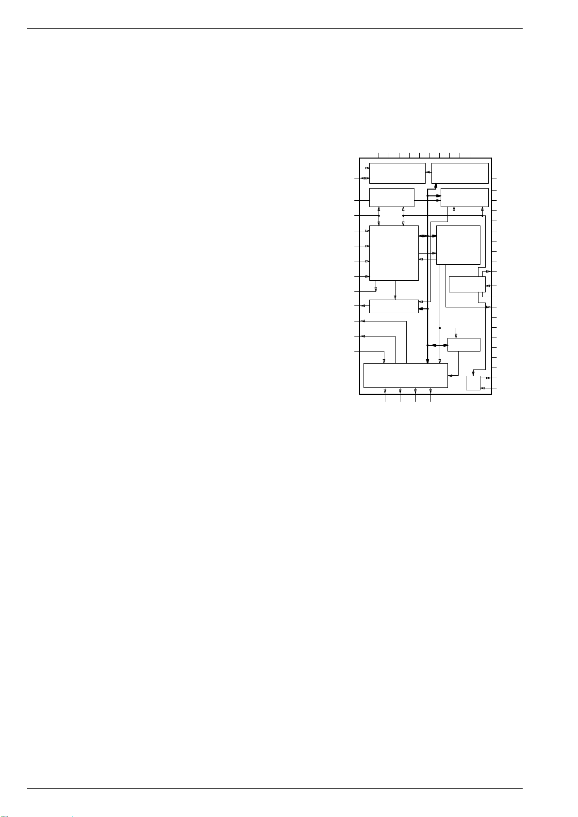
Descriptions TVR 3710 …, TVR 5100 …,TVR 5500 …
the "IN/OUT" circuit stage to the TV Signal Electronics and the EUROAV socket respectively.
On "LP" mode, switchover of the equalizing circuit is carried out by the
switch EP CTL.
3.7.4 Muting Circuit
The mute command (MTA) from the deck computer IC7410-(40) mutes
the audio outputs of IC7601 in all functions, with the exception of
playback and record, and also in the case of servo faults. For this, the
IC7601 obtains the mute command "MTA" via pin 22 (HIGH active).
4. Teletext "DOS" (TXT)
Function Overview
The DOS unit contains a Test Pattern / Data Generator and the VPS/
PDC/Teletext processing stage with IC7881 or IC7880 (with VPS and
PDC processing) being the heart of it. The following description refers
to IC7880. This IC7880, named IVT (Integrated Video-Input-Processor
and Teletext) includes the following function groups:
– Data Slicer
The adaptive data slicer extracts the VPS/PDC/teletext data from
the CCVS signal (VTV) fed in via IC7880-(8). For this, the video
signal is taken to an A/D converter. The text data is then separated
and the appropriate clock (6.9375MHz for PDC/Teletext and
2.5MHz for VPS ) is generated from the digitised video signal. The
black level of the CCVS signal is stored by C2888 at IC7880-(7). The
reference current for analog signal processing is derived via
IC7880-(9).
– Clock-PLL
The free-running 27MHz oscillator frequency is determined by the
quartz Q1800 at IC7880-(2…4) and is used first of all for the A/D
converter. Secondly, a digital PLL generates from it the basic
frequencies 6MHz, 1MHz, and 15.625kHz. The generated line
frequency is then fed to a phase comparator along with the line sync
signals separated from the CCVS signal. The characteristic of the
digital loop filter which follows is influenced by a control register and
the 6MHz oscillator is controlled accordingly. By this method, all
frequencies generated in the IVT are synchronized to the line
frequency of the incoming CCVS signal. In unsynchronized condi-
tion (eg. test pattern) no phase comparison takes place.
–I2C-bus Interface
This interface permits the central computer (IC7880) to control all
operations and also to read data into and out of each storage
location of the page memory.
– Control Logic
The control logic consists of various counters, gate circuits and
control registers which can be controlled via the I2C-bus. The control
logic is supplied with the internally generated 6MHz, 1MHz, H and
V-frequency pulses. In this way, the sync signal (IC7880-(12)), the
pixel clock for the character generator, and the control signals for the
page memory interface are produced among others.
– Data Acquisition
During the lines 16 for VPS, 2…22 and 315…335 for PDC/Teletext
the control logic provides a so-called data input window. The
acquisition circuit identifies the corresponding data by a determined
frame code. Subsequently, the data is subjected to a serial/parallel
conversion and an error detection or correction. When the user calls
up a text page a register with the page number is loaded via the I2C-
bus. The acquisition circuit then compares all incoming page num-
bers with the requested page and initializes the storage of the page
in the page memory.
– Page Memory
The 8k x 8-DRAM is used to store up to 8 teletext pages as well as
the PDC and VPS data.
– Character Generator
There are 256 different characters. Each of these characters is
allocated a 8bit data word. Apart from 32 control characters, the set
consists of graphic or alphanumeric characters composed in the
form of a raster point matrix of 12 horizontal and 10 vertical points.
The characters are stored in the Character ROM in the IVT. The line-
coupled 1MHz clock is used to switch the addresses fed in to the
page memory. The 8bit code representing the respective character
in turn forms one part of the address fed in to the character ROM. The
other part is produced by a line counter. The result is a 12bit data
word corresponding to the brightness information and is present at
the output of the ROM after every 1µs. This data word is entered into
a shift register and is read out at a 12MHz pixel clock derived from
the 6MHz clock. The corresponding R/G/B signals are available at
the push-pull outputs IC7880-(15…17). The maximum output level
of the R/G/B signals is determined by the voltage present on
IC7880-(18). The blank signal from IC7880-(19) is used to control
the insertion of the R/G/B signals in IC7200 within the TV Signal
Electronics (signal chassis).
IC7880
SAA5281
26 27 28 29 30 31 32 33 34 35
23
24
Clamp
AD-Conversion
8
7
Sync separation
and processing
9
11
Digital PLL
13
12
21
ODD/EVEN OR DV
20
22
18
Character Generator Buffers
Character ROM
15 16 17
19
Control RegistersI2C Businterface
Data slicing
and Acquisition
Acquisition
and Display
Line Counters
Oscillator
8k Memory
10
1
4
56
14
25
48
47
46
45
2
3
4
44
43
42
41
40
39
38
37
/2
36
2 - 16 GRUNDIG Service
k
Page 34
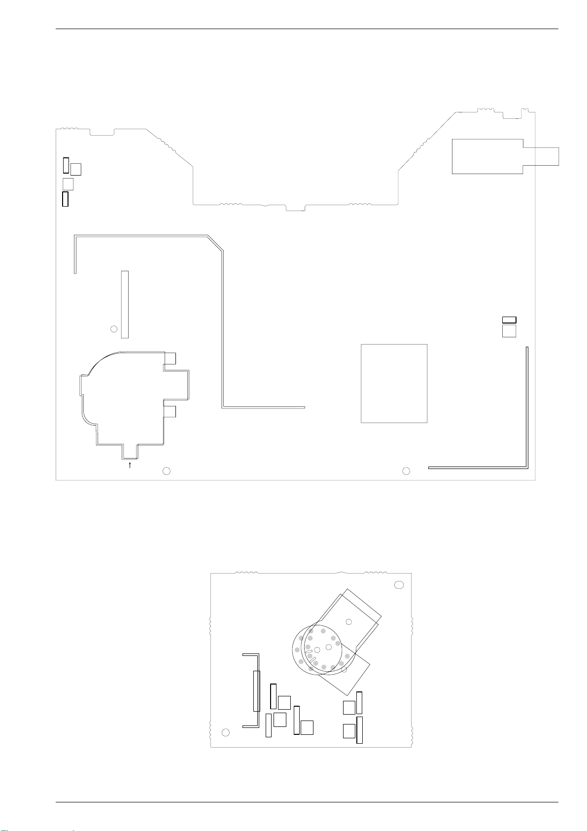
TVR 3710 …, TVR 5100 …, TVR 5500 … Abgleichlageplan / Location of Adjustment Controls
Abgleichlageplan / Location of Adjustment Controls
1. Leistungs-Chassis / Power Chassis (PLSP)
3524
v-shift
3523
v-amp
1
1925
5550
5551
FOCUS
SCREEN
2. Bildrohrplatte / Tube PCB
Ubat
3358
1
9
6
5
1
9
6
6
B
R
R
G
B
1
9
6
1
3921
BLUE-Gain
3919
GREEN-Gain
7900
3917
BLUE-Cutoff
3920
RED-Cutoff
G
3918
GREEN-Cutoff
GRUNDIG Service 3 - 1
Page 35
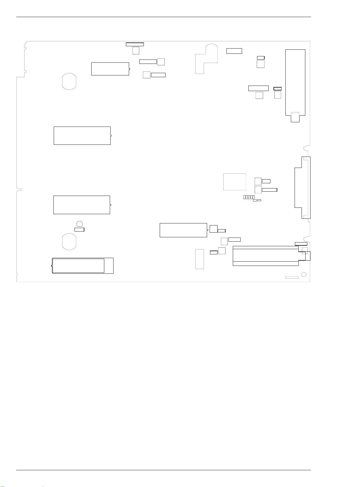
Abgleichlageplan / Location of Adjustment Controls TVR 3710 …, TVR 5100 …, TVR 5500 …
3. Signal Chassis (PSSP2)
32
33
48
(40)
1
SYNC-FREQU.
3010
3029
3027
PAL-CURR.
26
7200
27
1
5705
AFC1
52
3729
3712
AGC1
21
7051
22
32
7410
33
7801
2814
1
64
1
64
SECAM-CURR.
1
42
CLOCK
7880
)(
)(
7881
25
(21)
20
24
1902
L’-ADJ1
1
TDA9812:L’ADJ2
TDA9800:PHASE
AFC2
5303
3322
3618
3606
BIAS
PB-LEVEL
3600
1701(1702)
1301
AGC2
3341
1915
H-SHIFT
3206
3 - 2 GRUNDIG Service
Page 36
TVR 3710 …, TVR 5100 …, TVR 5500 … Abgleichvorschriften
D
Abgleichvorschriften
1. Leistungs-Chassis (PLSP)
Meßgeräte / Meßmittel: Digitalvoltmeter, Farbgenerator
Abgleich Vorbereitung Abgleichvorgang
1. Betriebsspannung,
R3358 (Ubat)
2. Fokusabgleich,
FOCUS
3. Bild "Vertikal",
R3523 (V-amp)
R3524 (V-shift)
Programm AV anwählen und kein Signal einspeisen.
Helligkeit und Kontrast "Minimum"
Digitalvoltmeter:.................................................. 1925-(2)
Gittertestbild einspeisen.
FuBK-Testbild einspeisen.
Spannung mit R3358 (Ubat) entsprechend dem Gerät einstellen. TVR3710… 100,9V
TVR5100… 117,8V
TVR5500… 82,6V
Fokusregler (FOCUS) am Zeilentrafo auf schärfste Gitter-
linien einstellen.
Mit den Reglern R3523 (V-amp) und R3524 (V-shift) das Bild
so einstellen, daß sich ein Kreis ergibt, und oberhalb und
unterhalb des Kreises noch 1/2 Gitter zu sehen sind.
2. Bildrohrplatte
Meßgeräte / Meßmittel: Digitalvoltmeter, Farbgenerator
Abgleich Vorbereitung Abgleichvorgang
1. Schwarzwert,
SCREEN
R3920 (RED-Cutoff)
R3918 (GREEN-Cutoff)
R3917 (BLUE-Cutoff)
2. Weißabgleich,
R3919 (GREEN-Gain)
R3921 (BLUE-Gain)
Folgende Einstellungen im betriebswarmen Gerätezustand
(ca. 15 Minuten nach dem Einschalten) durchführen:
– Kontrast "84% = OSD-Skala-Maximum minus 4 Teilstriche"
– Helligkeit "50%"
– Schirmgitterregler (SCREEN) "Linksanschlag"
– R3919 und R3921 "Mittelstellung"
– Schwarztestbild an der AV-Buchse einspeisen.
– Entsprechend dem Gerät jeweils folgende Werte mit den
Cutoff-Reglern R3920, R3918 und R3917 an den R-, Gund B-Eingängen der Bildröhre einstellen:
TVR 3710 … / TVR 5100 …: 115V
TVR 5500 …: 140V
Graustufentestbild einspeisen.
Helligkeit mit dem Schirmgitterregler (SCREEN) am
Zeilentrafo so einstellen, bis der Strahl gerade wieder
unsichtbar ist. Diese Helligkeitseinstellung ist nun genauso an den einzelnen Kathoden vorzunehmen, mit den
Reglern R3920 (RED-Cutoff), R3918 (GREEN-Cutoff) und R3917
(BLUE-Cutoff).
R3919 (GREEN-Gain) und R3921 (BLUE-Gain) so einstellen,
daß keine Verfärbungen in den Graubalken zu erkennen
sind.
3. Signal-Chassis (PSSP2)
3.1 Signal-Chassis – TV-Signalelektronik (TV)
Meßgeräte / Meßmittel: Digitalvoltmeter, Oszilloskop, Farbgenerator
Abgleich Vorbereitung Abgleichvorgang
1. Demodulatorkreis
PAL, L5705 (AFC1)
SECAM-L,
R3729 (L´ADJ1)
2. Tuner-Regelspannungseinsatz,
R3712 (AGC1)
3. Bildposition
"Horizontal",
R3206 (H-SHIFT)
Tuner 1701/1702-(5) mit Masse (GND) verbinden.
Digitalvoltmeter:.................. Bedieneinheit – IC7801-(24)
Empfangseinstellung: Norm BG (PAL)
Farbgenerator 38,9MHz, 35mV
Empfangseinstellung: Norm L (SECAM), Band 1 (Kanal 04)
Farbgenerator 33,95MHz, 35mV
R3712 "Linksanschlag"
Weißtestbild ohne Tonträger (UHF-Bereich, Kanal 24, Antennenpegel 67dBµV) in betriebswarmes Gerät einspeisen.
Oszilloskop: .................................. Tuner 1701/1702-(17)
FuBK-Testbild einspeisen.
an Tuner 1701/1702-(17)
eff
an Tuner 1701/1702-(17)
eff
Spannung mit L5705 (AFC1) auf 2,5V ±0,2V einstellen.
Spannung mit R3729 (L´ADJ1) auf 2,5V ±0,2V einstellen.
Masseverbindung entfernen.
Bei bestücktem TDA8361/N5 (IC7200):
Spannung mit R3712 (AGC1) auf 500mVSS -1dB einstellen.
Bei bestücktem TDA8362/N5 (IC7200):
Spannung mit R3712 (AGC1) auf 400mVSS -1dB einstellen.
Mit R3206 (H-SHIFT) so einstellen, daß die nicht mehr sichtbaren Bereiche des Bildes links und rechts symmetrisch
sind.
3.2 Signal-Chassis – Bedieneinheit (CO)
Meßgeräte / Meßmittel: Frequenzzähler
Abgleich Vorbereitung Abgleichvorgang
1. Uhr, C2814 (CLOCK)
IC7801-(7) und IC7801-(64) mit 1kΩ verbinden.
IC7801-(28) mit Masse (GND) verbinden.
Frequenzzähler:.............................................. IC7801-(7)
Gerät mit dem Netz verbinden.
Periodendauer mit C2814 (CLOCK) auf 122000ns ±0,035ns
abgleichen.
1kΩ-Widerstand und Masseverbindung entfernen.
GRUNDIG Service 3 - 3
j
Page 37
Abgleichvorschriften TVR 3710 …, TVR 5100 …, TVR 5500 …
3.3 Signal-Chassis – Laufwerksteuerung / Deck-Elektronik (DE)
Meßgeräte / Meßmittel: Testcassette
Abgleich Vorbereitung Abgleichvorgang
1. Kopfradlagengeber (GAP)
Testcassette einlegen und Service-Funktion aufrufen:
– Tasten
(Wiedergabe) am Gerät in dieser Reihenfolge drük-
¢e
ken und für mindestens 5s gedrückt halten.
– Mit einer der Taste der Fernbedienung G die Service-
ebene "SERVICE CONTROL" aufrufen.
– Mit den Tasten der Fernbedienung ]| die Funktion
"GAP POSITION" anwählen.
(STOP) auf der Fernbedienung und
¢ ■
Testcassette wiedergeben und eine der Tasten x /
drücken.
Bei erfolgreich durchgeführtem Abgleich schaltet das Gerät
in den Standby-Betrieb.
Bei nicht erfolgreich durchgeführtem Abgleich wirft das
Gerät die Testcassette aus.
Ursachen: Testcassette, Kopfscheibe oder technischer
Defekt (z.B. µC)
c
3.4 Signal-Chassis – Empfangseinheit 2 (TU2)
Meßgeräte / Meßmittel: Digitalvoltmeter, Oszilloskop
Abgleich Vorbereitung Abgleichvorgang
1. Demodulatorkreis
PAL, L5303 (AFC2)
SECAM-L,
R3322 (L´ADJ2)
2. Tuner-Regelspannungseinsatz,
R3341 (AGC2)
Tuner 1301-(5) mit Masse (GND) verbinden.
Digitalvoltmeter:......... Laufwerksteuerung – IC7410-(61)
Empfangseinstellung: Norm BG (PAL)
Farbgenerator 38,9MHz, 35mV
Empfangseinstellung: Norm L (SECAM), Band 1 (Kanal 04)
Farbgenerator 33,95MHz, 35mV
R3341 "Rechtsanschlag"
Weißtestbild ohne Tonträger (UHF-Bereich, Kanal 24, Antennenpegel 67dBµV) in betriebswarmes Gerät einspeisen.
Oszilloskop: ........................................... Tuner 1301-(17)
an Tuner 1301-(17)
eff
........ Tuner 1301-(17)
eff
Spannung mit L5303 (AFC2) auf 2,5V ±0,2V einstellen.
Spannung mit R3322(L´ADJ2) auf 2,5V ±0,2V einstellen.
Masseverbindung entfernen.
Bei bestücktem TDA9800T/V3 (IC7300):
Spannung mit R3341 (AGC2) auf 500mVSS -1dB einstellen.
Bei bestücktem TDA9812T (IC7301):
Spannung mit R3341 (AGC2) auf 400mVSS -1dB einstellen.
3.5 Signal-Chassis – Video/Chroma (VS)
Meßgeräte / Meßmittel: Leere Cassette, Oszilloskop mit Tastkopf 10:1, Frequenzzähler, Farbgenerator
Abgleich Vorbereitung Abgleichvorgang
1.Sync-Frequenz,
R3010(SYNC-FREQU.)
2. Chroma-Aufsprechpegel
PAL,
R3029 (PAL-CURR.)
SECAM-L,
R3027 (SECAM-CURR.)
AV-Aufnahme ohne Eingangssignal
Frequenzzähler:........................ Steckerkontakt 1902-(2)
IC7051-(2) über 150Ω und 22µH mit +5V verbinden.
Oszilloskop: .............................. Steckerkontakt 1902-(2)
PAL-Rotflächentestbild mit 75% Sättigung an der AVBuchse einspeisen und aufnehmen.
SECAM-L-Rotflächentestbild mit 75% Sättigung an der
AV-Buchse einspeisen und aufnehmen.
Frequenz mit R3010 (SYNC-FREQU.) auf 3,8MHz ±10kHz
einstellen.
Chroma-Signal mit R3029 (PAL-CURR.) auf 85mVss (-12,5dB
des FM-Signales) einstellen.
Spannung mit R3027 (SECAM-CURR.) auf 55mVss (-17dB des
FM-Signales) einstellen.
150Ω-Widerstand und 22µH-Spule entfernen.
3.6 Signal-Chassis – Standardton (AL)
Meßgeräte / Meßmittel: Leere Cassette, NF-Millivoltmeter
Abgleich Vorbereitung Abgleichvorgang
1. Vormagnetisierung
(70kHz), R3618(BIAS)
1.1 Frequenzgang
2. Wiedergabepegel,
R3606 (PB-LEVEL)
Beliebiges Signal aufzeichnen.
Mit NF-Voltmeter Spannungsabfall über R3600 messen.
–FBAS-Signal über die AV-Buchse, Kontakt 20 einspeisen.
– Audio-Signal 50mV
Buchse, Kontakt 2 oder 6 einspeisen.
–Aufnahme mit jeweils ca. 1 Minute 400Hz- und 8kHz-Ton
durchführen. Anschließend diese Aufnahme wiedergeben.
–NF-Millivoltmeter an der AV-Buchse, Kontakte 1 oder 3
anschließen.
Tongenerator (1kHz / 0,5V
.......................................... AV-Buchse, Kontakt 2 oder 6
Aufnahme (Normalplay).
Wiedergabe dieser Aufnahme.
vom Tongenereator an der AV-
eff
): ..........................................
eff
Spannungsabfall an R3600 mit R3618 (BIAS) auf 15mV
einstellen und Frequenzgang prüfen.
Das Spannungsverhältnis von 400Hz zu 8kHz darf nicht
größer als 1:0,7 bzw. 0,7:1 (±3dB) sein. Überschreitet das
Spannungsverhältnis diese Grenzen, ist die Vormagnetisierung zu verändern:
Wiedergabespannung bei 8kHz…
Ausgangsspannung mit R3606 (PB-LEVEL) auf 0,5V
stellen.
… vergrößern: "BIAS" verringern.
… verkleinern: "BIAS" erhöhen.
ein-
eff
eff
3 - 4 GRUNDIG Service
j
Page 38
TVR 3710 …, TVR 5100 …, TVR 5500 … Adjustment Procedures
GB
Adjustment Procedur es
1. Power Chassis (PLSP)
Test Equipment / Aids: Digital Voltmeter, Colour Generator
Alignment Preparation Alignment Procedure
1. 110V operating
voltage
R3358 (Ubat)
2. Focus adjustment
FOCUS
3. Vertical picture
R3523 (V-amp)
R3524 (V-shift)
Select AV programme position without feeding in a signal.
Set contrast and brightness to "minimum".
Digital voltmeter:................................................. 1925-(2)
Feed in a crosshatch pattern signal.
Feed in a FuBK test pattern.
With R3358 (Ubat) set the following voltage according to the
different models: TVR3710... 100.9V
TVR5100... 117.8V
TVR5500... 82.6V
Adjust the focus control (FOCUS) on the line transformer
to obtain the sharpest crosshatch pattern possible.
With the adjustment controls R3523 (V-amp) and R3524
(V-shift) adjust the picture to obtain a round circle with half
a square of the pattern being visible at the top and at the
bottom of the circle.
2. Tube PCB
Test Equipment / Aids: Digital Voltmeter, Colour Generator
Alignment Preparation Alignment Procedure
1. Black level
SCREEN
R3920 (RED-Cutoff)
R3918 (GREEN-Cutoff)
R3917 (BLUE-Cutoff)
2. White balance
R3919 (GREEN-Gain)
R3921 (BLUE-Gain)
Allow the set to warm up (for approx. 15 minutes after
switching on) and carry out the following adjustments:
– Contrast "84% = maximum minus 4 divisions on OSD scale"
– Brightness "50%"
– Screen grid adjustment control (SCREEN) "left stop"
– R3919, R3921 "center position".
–
Feed a black test pattern into the AV socket.
– With the cutoff controls R3920, R3918 and R3917, set the
following levels at the R, G, and B inputs of the picture
tube dependent on the TVR model:
TVR 3710 … / TVR 5100 …: 115V
TVR 5500 …: 140V
Feed in a grey scale pattern.
Turn the screen adjustment control (SCREEN) on the
line transformer until the beam just becomes invisible
again. Repeat this brightness ajdustment at the individual
cathodes using the respective controls R3920 (RED-Cutoff),
R3918 (GREEN-Cutoff) and R3917 (BLUE-Cutoff).
Set R3919 (GREEN-Gain) and R3921 (BLUE-Gain) so that no
discolouration is visible in the grey scale.
3. Signal Chassis (PSSP2)
3.1 Signal Chassis – TV Signal Electronics (TV)
Test Equipment / Aids: Digital Voltmeter, Oscilloscope, Colour Generator
Alignment Preparation Alignment Procedure
1. Demodulator
circuit
PAL, L5705 (AFC1)
SECAM-L,
R3729 (L´ADJ1)
2. Start-up of the
tuner control
voltage
R3712 (AGC1)
3. Horizontal position
R3206 (H-SHIFT)
Connect tuner 1701/1702-(5) to GND.
Digital voltmeter:............ keyboard control – IC7801-(24)
Reception: PAL-BG
Colour generator 38.9MHz, 35mV
Reception: SECAM-L, band 1 (channel 04)
Colour generator 33.95MHz, 35mV
R3712 to "left stop"
Feed in a white test pattern without sound carrier (UHF range,
channel 24, 67dBµV aerial signal) into the warmed up TVR .
Oscilloscope: ................................. tuner 1701/1702-(17)
Feed in a FuBK test pattern.
to tuner 1701/1702-(17)
rms
to tuner 1701/1702-(17)
rms
Adjust the voltage to 2.5V ±0.2V with L5705 (AFC1).
Adjust the voltage to 2.5V ±0.2V with R3729(L´ADJ1).
Disconnect GND.
With TDA8361/N5 (IC7200) fitted:
With R3712 (AGC1) set the voltage to 500mVpp -1dB.
With TDA8362/N5 (IC7200) fitted:
With R3712 (AGC1) set the voltage to 400mVpp -1dB.
Adjust with R3206 (H-SHIFT) so that the no longer visible edges
at the right and left of the picture are symmetric to the screen.
3.2 Signal Chassis – Keyboard Control Unit (CO)
Test Equipment / Aids: Frequency Counter
Alignment Preparation Alignment Procedure
1. Clock,
C2814 (CLOCK)
Connect IC7801-(7) and IC7801-(64) via a 1kΩ resistor.
Connect IC7801-(28) to GND.
Frequency counter:.........................................IC7801-(7)
Connect the TVR to the mains.
Adjust the period to 122000ns ±0.035ns with C2814
(CLOCK).
Remove the 1kΩ resistor and the GND connection.
GRUNDIG Service 3 - 5
k
Page 39
Adjustment Procedures TVR 3710 …, TVR 5100 …, TVR 5500 …
3.3 Signal Chassis – Deck Control / Deck Electronic (DE)
Test Equipment / Aids: Test Cassette
Alignment Preparation Alignment Procedure
1. Head switching
position (GAP)
Load the test cassette and call up the Service Function:
– Press button
(playback) on the local keyboard and hold them down for
¢ e
5s at least.
– With button G on the remote control call up the "SERVICE
CONTROL" function.
– With button ]| on the remote control call up the "GAP
POSITION" function.
(STOP) on the remote control followed by
¢ ■
Play back the test cassette and press one of the buttons x /
on the remote control.
On successful alignment the TVR switches to stand-by.
If the procedure was not successful, the TVR ejects the test
cassette.
Causes: Test cassette, headwheel or technical defect
(e.g. µC)
c
3.4 Signal Chassis – Frontend 2 (TU2)
Test Equipment / Aids: Digital Voltmeter, Oscilloscope
Alignment Preparation Alignment Procedure
1. Demodulator
circuit
PAL, L5303 (AFC2)
SECAM-L,
R3322 (L´ADJ2)
2. Start-up of the
tuner control
voltage
R3341 (AGC2)
Connect tuner 1301-(5) to GND.
Digital voltmeter:....................... tape deck – IC7410-(61)
Reception: PAL-BG
Colour generator 38.9MHz, 35mV
Reception: SECAM-L, band 1 (channel 04)
Colour generator 33.95MHz, 35mV
R3341 "fully clockwise"
Feed in a white test pattern without sound carrier (UHF range,
channel 24, 67dBµV aerial signal) into the warmed up TVR.
Oscilloscope: .......................................... tuner 1301-(17)
to tuner 1301-(17)
rms
.... tuner 1301-(17)
rms
With L5303 (AFC2) set the voltage to 2.5V ±0.2V.
With R3322 (L´ADJ2) set the voltage to 2.5V ±0.2V.
Remove the ground connection.
With TDA9800T/V3 (IC7300) fitted:
With R3341 (AGC2) set the voltage to 500mVpp -1dB.
With TDA9812T (IC7301) fitted:
With R3341 (AGC2) set the voltage to 400mVpp -1dB.
3.5 Signal Chassis – Video/Chroma (VS)
Test Equipment / Aids: Blank Cassette, Oscilloscope with 10:1 Test Probe, Frequency Counter, Colour Generator
Alignment Preparation Alignment Procedure
1.Sync frequency
R3010(SYNC-FREQU.)
2. Chroma recording
current
PAL
R3029 (PAL-CURR.)
SECAM-L
R3027 (SECAM-CURR.)
AV recording without input signal
Frequency counter:...............connector contact 1902-(2)
Connect IC7051-(2) via 150Ω and 22µH to +5V supply.
Oscilloscope: ........................connector contact 1902-(2)
Feed in a PAL red raster test pattern with 75% saturation
into the AV socket and record it.
Feed in a SECAM-L red raster test pattern with 75%
saturation into the AV socket and record it.
With R3010 (SYNC-FREQU.) set the frequency to 3.8MHz
±10kHz.
With R3029 (PAL-CURR.) set the chroma signal to 85mV
(-12.5dB of the FM signal).
With R3027 (SECAM-CURR.) set the voltage to 55mVpp (-17dB
of the FM signal).
Remove the150Ω resistor and 22µH coil.
3.6 Signal Chassis – Standard Sound (AL)
Test Equipment / Aids: Blank Cassette, AF Voltmeter
Alignment Preparation Alignment Procedure
1. Bias (70kHz),
R3618 (BIAS)
1.1 Frequency
response
2. Playback level
R3606 (PB-LEVEL)
Record any signal.
Measure the voltage drop on R 3600 with AF voltmeter.
–Feed in a CCVS signal via AV socket, contact 20.
–Feed an audio signal of 50mV
the AV socket, contact 2 or 6.
– Record the 400Hz and 8kHz signals each for 1 min at
least. Afterwards play back these recordings.
–Connect an AF millivoltmeter to the AV socket, contact
1 or 3.
Sound generator (1kHz / 0.5V
.................................................AV socket, contact 2 or 6
Record (Normal Play).
Play this recording back.
from the AF generator to
rms
):....................................
rms
Adjust voltage drop on R3600 to 15mV
Check the frequency response.
The voltage ratio of 400Hz to 8kHz must not be higher than
1:0.7 or 0.7:1 (±3dB). If the voltage ratio exceeds these
limits, the bias must be corrected:
To increase the playback voltage at 8kHz: reduce "BIAS".
To reduce the playback voltage at 8kHz: increase "BIAS".
With R3606 (PB-LEVEL) set an output level of 0.5V
with R3618 (BIAS).
rms
rms
pp
3 - 6 GRUNDIG Service
k
Page 40
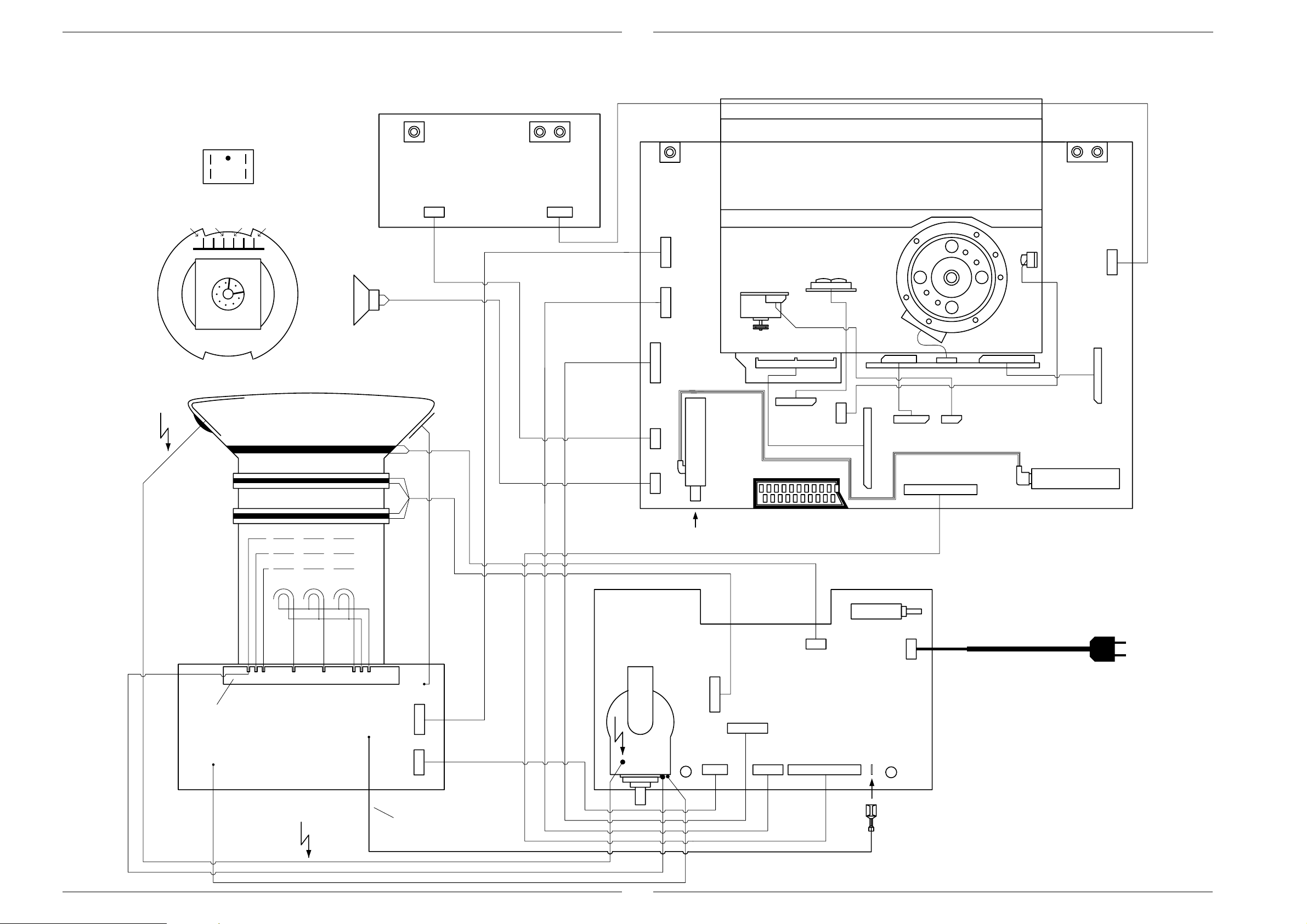
TVR 3710 …, TVR 5100 …, TVR 5500 … Platinenabbildungen und Schaltpläne / Layout of PCBs and Circuit Diagrams
Platinenabbildungen und Schaltpläne / Layout of the PCBs and Circuit Diagrams
Verdrahtungsplan / Wiring Diagram TVR 3710 …
TVR 3710 …, TVR 5100 …, TVR 5500 … Platinenabbildungen und Schaltpläne / Layout of PCBs and Circuit Diagrams
OPTION ( OTHER CONNECTION TERMANAL )
TOP
VDEFH (Yellow)
4
2
TOP
(Blue)
321
DEFLECTION COIL
Rear View
VDEFL (Green)
3
HDEF1 (Red)HDEF2 (Blue)
1
HDEF1VDEFL VDEFHHDEF2
(Red)(Green)
(Yellow)
4
65
PICTURETUBE
E.H.T
SPEAKER
1931
EARPHONE-JACK
1935
PH1
PH2
PH3
1
3
2
VIDEO-AUDIO-JACK
PLSP14
BUPI ( OPTION )
Front Cinch Board
Component side
1933
Cinch
1937
GND
VCI
4
3
GND
2
ACIM
1
1916
EARPHONE-JACK
1913
5
B
GNDTV
4
RFK 1
3
R
2
8V
1
G
1911
VDR
5
VFB
4
RFK 5
GNDTV
3
HDR
2
HFB
1
1912
7 8VSW
6
PROT
RFK 5
5
BCI
4
VCOMP
3
GND9A
9A
2
1
-7V
1971
RFK 5
3
PH1
2
PH2
1
PH3
1914
RFK 5
3
LS2
2
N.C.
1
LS1
Tuner 1
THREADING MOTOR
TMO1
N.C.
TMO2
3
2
1
1-1
1-1
TAS
15
INIT
LED
WTR
121314
RECP
FTA
10
11
1901
7
6
CTL1
CTL2
L4
WTL
5
AEH1
SCART
TURBO/ECO-WD
AUDIO-CONTROL-HEAD
CTL1
CTL2
AEH1
AEH2
APH
GND
ARH
L3
7
5
1
4
6
2
3
GNDM1
FG
CAP
CREV
14/9
GNDD
TAE
5STBY
4
AEH2
1915
789
3
APH
6
2
GND
5
1
ARH
1
4
2
3
L2
1
N.C.
RFK 5
2
MEH1
MEH2
3
1900
15
14
13
12
11
10
9
8
7
6
1905
5
4
3
2
1
TAS
INIT
LED
WTR
FTA
RECP
WTL
5STBY
TAE
GNDD
14/9
CREV
CAP
FG
GNDM1
PG/FG
14M2
GNDD
GNDM2
5D
REEL
L1 L6
5
1
4
6
2
3
HEAD AMPLIFIER
5
1
4
6
2
3
5D
14M2
REEL
GNDD
PG/FG
GNDM2
5STBY
STBY
33A
5A
GND5A
1
432
5D
GND5D
6
19031904
3
2
N.C.
TMO2
GNDM
GNDM
9
857
1
TMO1
14M2
14M2
11
10
14M1
12
14/9M1
13
ERASE-HEAD
SCANNER
CSYNC
5VAS
FMPV
GNDA
1
4106
2
3
1909
ENVC
5
TRIV
HSC
7
HP1
8
2
1
L8
FMRV
9
FRONT-CINCH-JACK
PSSP2
Familyboard PAL
Component side
MEH1
MEH2
GNDA
Tuner 2
only for 2 TUNER CONCEPT
1919
VCI
GND
GND
ACIM
1902
10
9
8
7
6
5
4
3
2
1
1918
1
2
3
4
GNDA
FMPV
5VAS
CSYNC
ENVC
TRIV
HSC
HP1
FMRV
GNDA
RFK 5
681
Vg1
Vg2
FOCUS
CRT CONNECTION SOCKET
1963
SCREEN
PLSP14
Picturetube-PCB
7
RED
Component side
1961
9
GREEN
10
345
BLUE
HEATER
GNDTV
GNDA
1964
AQUADAC
GNDTV
VRGB
GNDA
HEATER
AQUADAC
AQUADAC
B
R
8V
G
GROUND LEAD ( OPTION )
1962
1967
1969
Antenna Input
MAINS SWITCH
PLSP14
POWER - PCB
Component side
LINE OUTPUT TRANSFORMER
1
2
3
4
5
RFK 1
1
2
3
4
BTB
VDEFL
VDEFH
UBAT
HDEF2
110LOT
HDEF1
1925
1926
BTB
6
5
4
3
2
1
VRGB
1
2
GNDA
HEATER
3
-7V
7
RFK 5
AQUADAC
4
1923
GND9A
9A
6
5
VCOMP
BCI
3
4
RFK 5
PROT
1
2
1922
HDR
HFB
5
4
8VSW
GNDTV
3
VFB
2
VDR
1
RFK 1
5STBY
STBY
13
12
2
DEGC2
1924
33A
GND5A
11
10
RFK 5
1
DEGC1
1921
GND5D
5A
8
9
5D
7
GNDM
GNDM
6
5
14M2
4
1929
14M2
14M1
14/9M1
1
2
3
plugged on PCB
FASTON CONNECTOR
MACH
MACC
1001
2
1
LINE POWER CORD
E.H.T
FOCUS
SCREEN
GRUNDIG Service 4 - 1
GRUNDIG Service 4 - 2
Page 41
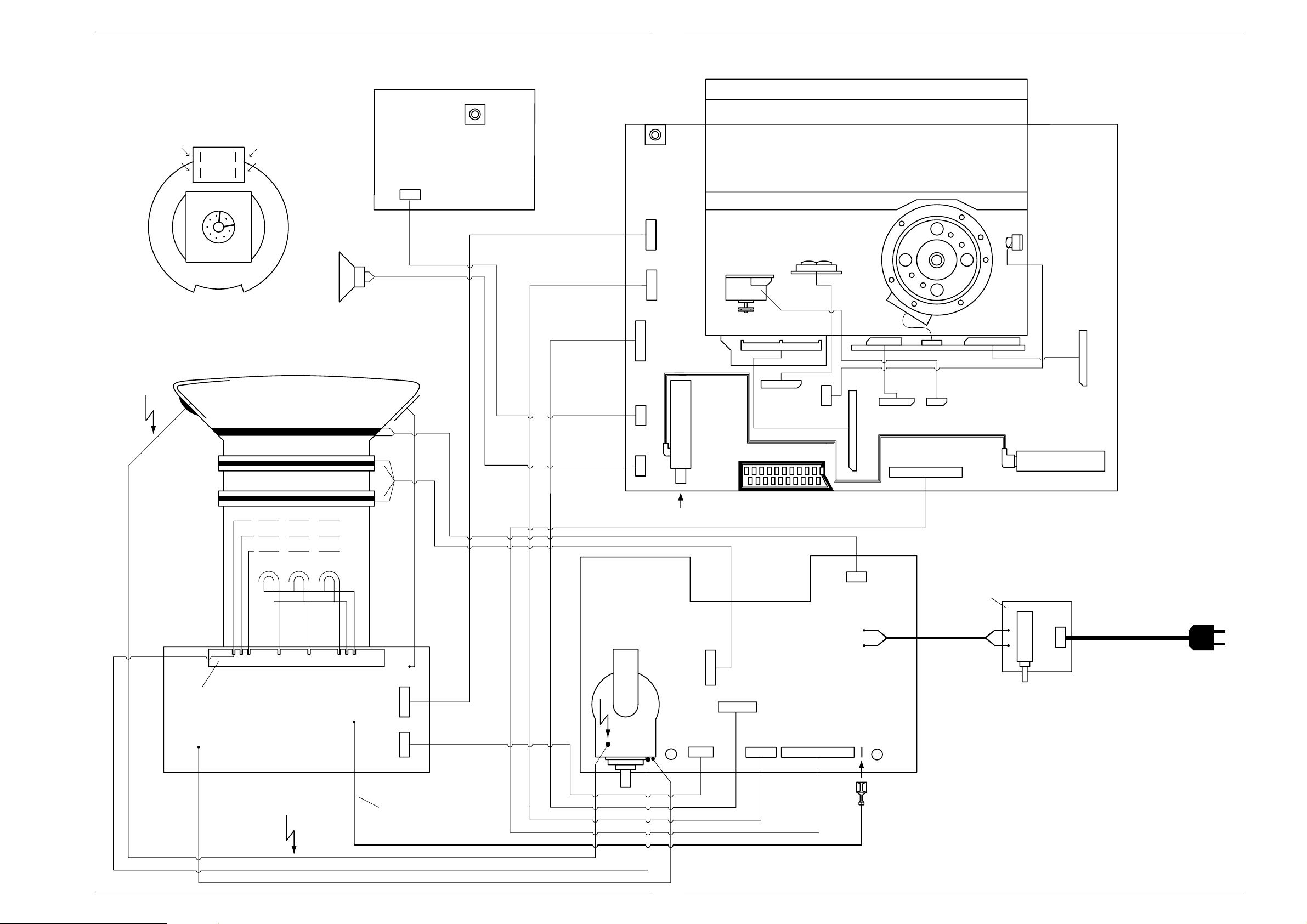
Platinenabbildungen und Schaltpläne / Layout of PCBs and Circuit Diagrams TVR 3710 …, TVR 5100 …, TVR 5500 … Platinenabbildungen und Schaltpläne / Layout of PCBs and Circuit Diagrams TVR 3710 …, TVR 5100 …, TVR 5500 …
Verdrahtungsplan / Wiring Diagram TVR 5100 …
VDEFH (Yellow)
E.H.T
TOP
43
2
DEFLECTION COIL
Rear View
HDEF1 (Red)HDEF2 (Blue)
1
VDEFL (Green)
PICTURETUBE
SPEAKER
1935
PH3
3
PLSP20
BUPI ( OPTION )
PH1
PH2
2
1
Front Jack Board
1931
EARPHONE-JACK
Component side
1916
EARPHONE-JACK
1913
5
B
4
GNDTV
RFK 1
3
R
2
8V
1
G
1911
VDR
5
VFB
4
RFK 5
GNDTV
3
HDR
2
HFB
1
1912
8VSW
7
6
PROT
BCI
5
RFK 5
4
VCOMP
GND9A
3
9A
2
1
-7V
1971
RFK 5
3
PH1
2
PH2
1
PH3
1914
RFK 5
3
LS2
2
N.C.
1
LS1
Tuner 1
THREADING MOTOR
TMO1
N.C.
TMO2
3
2
1
1-1
1-1
TAS
15
INIT
LED
WTR
121314
RECP
FTA
10
11
1901
7
6
CTL1
CTL2
L4
WTL
5
AEH1
SCART
TURBO/ECO-WD
AUDIO-CONTROL-HEAD
CTL1
CTL2
AEH1
AEH2
APH
GND
ARH
L3
7
5
1
4
6
2
3
GNDM1
FG
CAP
CREV
14/9
GNDD
TAE
5STBY
4
AEH2
1915
789
3
APH
6
2
GND
5
1
ARH
L2
4
3
N.C.
MEH1
MEH2
1
2
1
RFK 5
2
3
1900
15
14
13
12
11
10
9
8
7
6
1905
5
4
3
2
1
TAS
INIT
LED
WTR
FTA
RECP
WTL
5STBY
TAE
GNDD
14/9
CREV
CAP
FG
GNDM1
PG/FG
14M2
GNDD
GNDM2
5D
REEL
L1 L6
5
1
4
6
2
3
HEAD AMPLIFIER
5
1
4
6
2
3
5D
14M2
REEL
GNDD
PG/FG
GNDM2
5STBY
STBY
33A
5A
GND5A
1
432
5D
GND5D
6
3
2
N.C.
TMO2
GNDM
GNDM
9
857
19031904
1
TMO1
14M2
10
14M2
11
14M1
12
14/9M1
13
ERASE-HEAD
SCANNER
CSYNC
5VAS
FMPV
GNDA
1
4106
2
3
1909
ENVC
5
TRIV
HSC
7
HP1
8
L8
FMRV
9
PSSP2
Familyboard PAL
Component side
MEH1
2
MEH2
1
GNDA
Tuner 2
only for 2 TUNER CONCEPT
1902
10
9
8
7
6
5
4
3
2
1
GNDVS
FMPV
5VAS
CSYNC
ENVC
TRIV
HSC
HP1
FMRV
GNDVS
571
Vg1
Vg2
FOCUS
CRT CONNECTION SOCKET
1963
SCREEN
PLSP20
Picturetube-PCB
8
RED
1966 (1965)
Component side
6
GREEN
9
12
11
BLUE
GNDTV
10
HEATER
1964
GNDA
AQUADAC
GNDTV
HEATER
AQUADAC
8V
VRGB
GNDA
AQUADAC
B
R
G
GROUND LEAD ( OPTION )
1962
1967
1
2
3
4
5
1969
1
2
3
4
RFK 1
BTB
Antenna Input
PLSP20
POWER - PCB
Component side
LINE OUTPUT TRANSFORMER
VDEFL
VDEFH
UBAT
HDEF2
110LOT
HDEF1
1926
BTB
VRGB
1
1925
GNDA
HEATER
3
2
6
5
4
3
2
1
RFK 5
AQUADAC
4
-7V
7
1923
GND9A
9A
5
6
VCOMP
BCI
4
3
RFK 5
PROT
8VSW
2
1922
HFB
5
1
HDR
4
GNDTV
VFB
2
3
VDR
1
5STBY
STBY
13
12
33A
GND5A
11
10
RFK 5
1921
GND5D
5A
8
9
5D
7
RFK 1
GNDM
GNDM
6
5
14M2
4
2
1
1924
DEGC1
DEGC2
1015
1013
1929
14M2
14M1
14/9M1
1
2
3
plugged on PCB
FASTON CONNECTOR
PLSP20
Mainsswitch-PCB
Component side
MAINS SWITCH
1002
MACH
2
MACC
1
RFK 1
LINE POWER CORD
E.H.T
FOCUS
SCREEN
4 - 3 GRUNDIG Service 4 - 4 GRUNDIG Service
Page 42
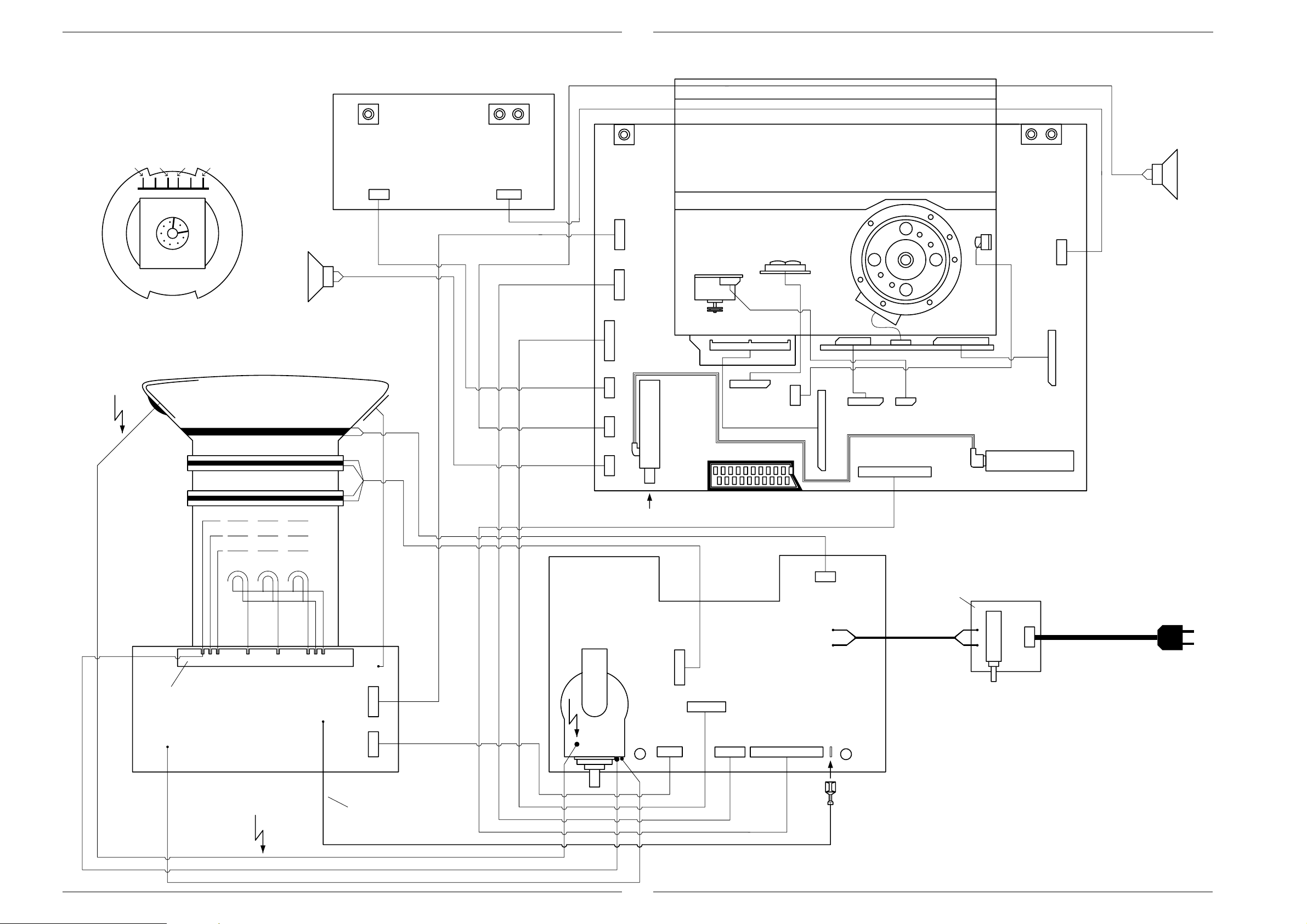
TVR 3710 …, TVR 5100 …, TVR 5500 … Platinenabbildungen und Schaltpläne / Layout of PCBs and Circuit Diagrams
Verdrahtungsplan / Wiring Diagram TVR 5500 …
TVR 3710 …, TVR 5100 …, TVR 5500 … Platinenabbildungen und Schaltpläne / Layout of PCBs and Circuit Diagrams
DEFLECTION COIL
E.H.T
TOP
Rear View
1931
EARPHONE-JACK
VDEFHHDEF1HDEF2VDEFL
(Yellow)(Red)(Blue)(Green)
654321
1935
PLSP21
PH1
PH2
PH3
3
1
2
Front Cinch Board
BUPI ( OPTION )
Component side
SPEAKER 1
PICTURETUBE
1933
VIDEO-AUDIO-JACK
Cinch
1937
GND
ACIM
VCI
GND
4
1
3
2
1916
EARPHONE-JACK
1913
5
B
4
GNDTV
RFK 1
3
R
2
8V
1
G
1911
VDR
5
VFB
4
RFK 5
GNDTV
3
HDR
2
HFB
1
1912
8VSW
7
6
PROT
BCI
5
RFK 5
4
VCOMP
GND9A
3
9A
2
1
-7V
1971
RFK 5
PH1
3
2
PH2
1
PH3
1970
RFK 5
3
LS2
2
N.C.
1
LS1
1914
RFK 5
3
LS2
2
N.C.
1
LS1
Tuner 1
THREADING MOTOR
TMO1
N.C.
TMO2
3
2
1
1-1
1-1
TAS
15
INIT
LED
WTR
121314
RECP
FTA
10
11
1901
7
6
CTL1
CTL2
L4
WTL
5
AEH1
SCART
TURBO/ECO-WD
AUDIO-CONTROL-HEAD
CTL1
CTL2
AEH1
AEH2
APH
GND
ARH
L3
7
5
1
4
6
2
3
GNDM1
FG
CAP
CREV
14/9
GNDD
TAE
5STBY
4
AEH2
1915
789
3
APH
6
2
GND
5
1
ARH
L2
4
MEH1
MEH2
3
N.C.
1
2
1
RFK 5
2
3
1900
15
14
13
12
11
10
9
8
7
6
1905
5
4
3
2
1
TAS
INIT
LED
WTR
FTA
RECP
WTL
5STBY
TAE
GNDD
14/9
CREV
CAP
FG
GNDM1
PG/FG
14M2
GNDD
GNDM2
5D
REEL
L1 L6
5
1
4
6
2
3
HEAD AMPLIFIER
5
1
4
6
2
3
5D
14M2
REEL
GNDD
PG/FG
GNDM2
5STBY
STBY
33A
GND5D
5A
GND5A
1
432
6
5D
19031904
3
2
N.C.
TMO2
GNDM
GNDM
9
857
1
TMO1
14M2
10
14M2
11
14M1
12
14/9M1
13
ERASE-HEAD
SCANNER
CSYNC
5VAS
FMPV
GNDA
1
4106
2
3
1909
ENVC
5
TRIV
HSC
7
HP1
8
L8
FMRV
9
FRONT-CINCH-JACK
PSSP2
Familyboard PAL
Component side
MEH1
2
MEH2
1
GNDA
Tuner 2
only for 2 TUNER CONCEPT
1919
ACIM
VCI
GND
GND
1902
10
9
8
7
6
5
4
3
2
1
1918
GNDVS
FMPV
5VAS
CSYNC
ENVC
TRIV
HSC
HP1
FMRV
GNDVS
SPEAKER 2
1
RFK 5
2
3
4
571
Vg1
Vg2
FOCUS
CRT CONNECTION SOCKET
1963
SCREEN
PLSP21
Picturetube-PCB
8
RED
Component side
1965
6
GREEN
9
12
11
BLUE
GNDTV
10
HEATER
1964
GNDA
AQUADAC
GNDTV
VRGB
GNDA
HEATER
AQUADAC
AQUADAC
B
R
8V
G
GROUND LEAD ( OPTION )
1962
1967
1969
Antenna Input
2
VRGB
GNDA
1
2
1925
6
5
4
3
2
1
HEATER
AQUADAC
4
3
-7V
RFK 5
# 2563.
1923
GND9A
9A
5
7
6
VCOMP
BCI
4
3
RFK 5
PROT
8VSW
1
2
1922
HFB
5
HDR
4
GNDTV
VFB
2
3
VDR
1
5STBY
13
STBY
12
PLSP21
POWER - PCB
Component side
LINE OUTPUT TRANSFORMER
VDEFL
VDEFH
UBAT
HDEF2
110LOT
HDEF1
1
2
3
4
5
1
2
3
4
BTB RFK 1
1926
BTB
33A
11
RFK 5
1921
5A
GND5A
9
10
5D
GND5D
7
8
RFK 1
GNDM
6
DEGC2
1015
1013
1929
GNDM
14M2
14M2
14M1
14/9M1
1
5
2
4
3
plugged on PCB
FASTON CONNECTOR
1
1924
DEGC1
PLSP21
Mainsswitch-PCB
Component side
MAINS SWITCH
1002
MACH
2
MACC
1
RFK 1
LINE POWER CORD
E.H.T
FOCUS
SCREEN
GRUNDIG Service 4 - 5
GRUNDIG Service 4 - 6
Page 43
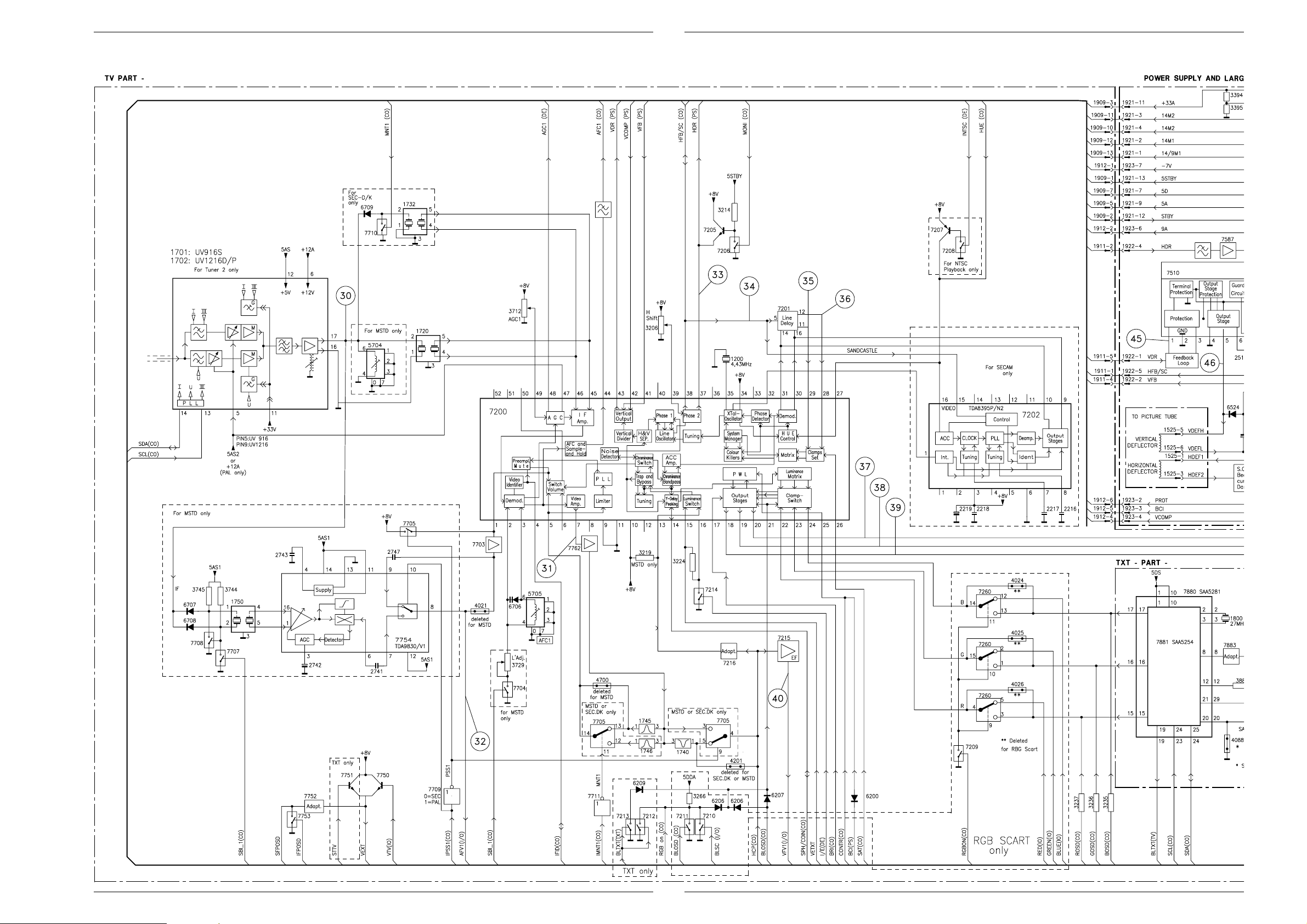
Platinenabbildungen und Schaltpläne / Layout of PCBs and Circuit Diagrams TVR 3710 …, TVR 5100 …, TVR 5500 … Platinenabbildungen und Schaltpläne / Layout of PCBs and Circuit Diagrams TVR 3710 …, TVR 5100 …, TVR 5500 …
Blockschaltplan / Block Circuit Diagram (TV)
Signal Chassis
Signal Chassis
4 - 7 GRUNDIG Service 4 - 8 GRUNDIG Service
Page 44
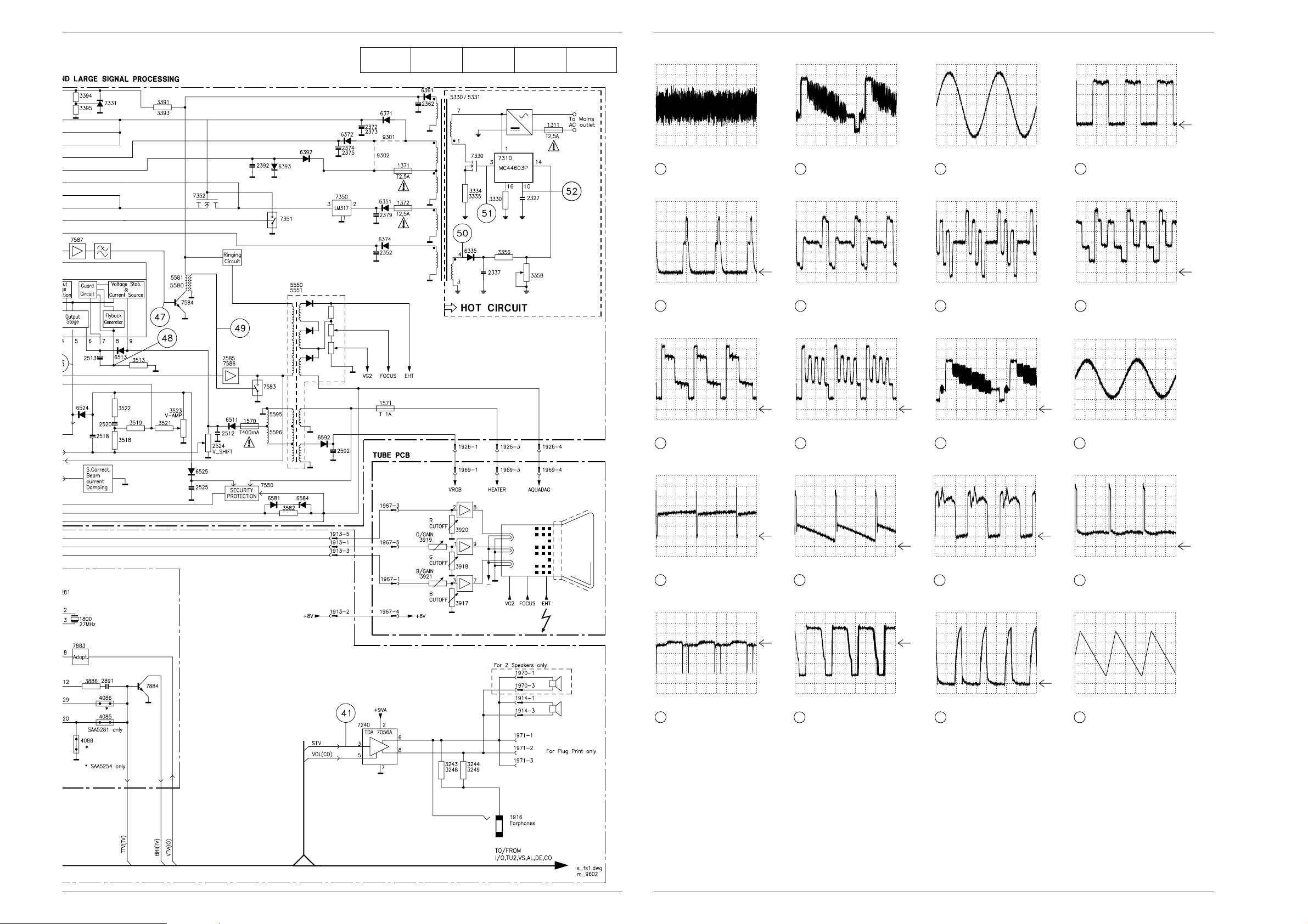
TVR 3710 …, TVR 5100 …, TVR 5500 … Platinenabbildungen und Schaltpläne / Layout of PCBs and Circuit Diagrams
AC, 200mV/Div, 20ms/Div
Tuner 1701/1702-(17)
TV
30
DC, 500mV/Div, 20µs/Div
0V
IC7200-(37), Connector 1922-(4)
TV
33
DC, 1V/Div, 20µs/Div
0V
IC7200-(38), Connector 1922-(5)
TV
34
DC, 500mV/Div, 20µs/Div
0V
IC7200-(20)
TV
37
DC, 500mV/Div, 20µs/Div
0V
IC7200-(19)
TV
38
DC, 1V/Div, 5ms/Div
0V
IC7510-(1)
TV
45
DC, 10V/Div, 5ms/Div
0V
IC7510-(5)
TV
46
DC, 5V/Div, 5ms/Div
0V
IC7510-(8)
TV
48
DC, 5V/Div, 20µs/Div
0V
T7583 – Basis
TV
49
DC, 10V/Div, 5µs/Div
0V
Trafo 5330-(4), 5331-(4)
PB
50
TVR 3710 …, TVR 5100 …, TVR 5500 … Platinenabbildungen und Schaltpläne / Layout of PCBs and Circuit Diagrams
(PLSP)
Reference
AL ..............P 4-65
BUPI ..........P 4-68
CO .............P 4-43
DE..............P 4-49
IO...............P 4-59
OHA...........P 4-69
PLSP .........P4-19
PSSP2.......P 4-37
TU2............P 4-55
T
ube PCB
...P 4-33
TV..............P 4-51
TXT............P 4-58
VS..............P 4-61
AC, 500mV/Div, 10µs/Div
IC7200-(7)
31
AC, 200mV/Div, 20µs/Div
IC7200-(29)
35
TV
TV
TV
AC, 200mV/Div, 200µs/Div
IC7754-(8)
32
AC, 200mV/Div, 20µs/Div
IC7200-(28)
36
TV
TV
TV
TV
DC, 500mV/Div, 20µs/Div
IC7200-(18)
39
0V
DC, 500mV/Div, 10µs/Div
T7215 – Emitter
40
0V
AC, 100mV/Div, 200µs/Div
IC7240-(3)
41
TV
0V
is
DC, 200mV/Div, 20µs/Div
T7584 – Basis
47
PB
STANDBY
0V
DC, 2V/Div, 5µs/Div
T7330 – Gate
51
AC, 500mV/Div, 10µs/Div
IC7310-(10)
52
GRUNDIG Service 4 - 9
GRUNDIG Service 4 - 10
Page 45
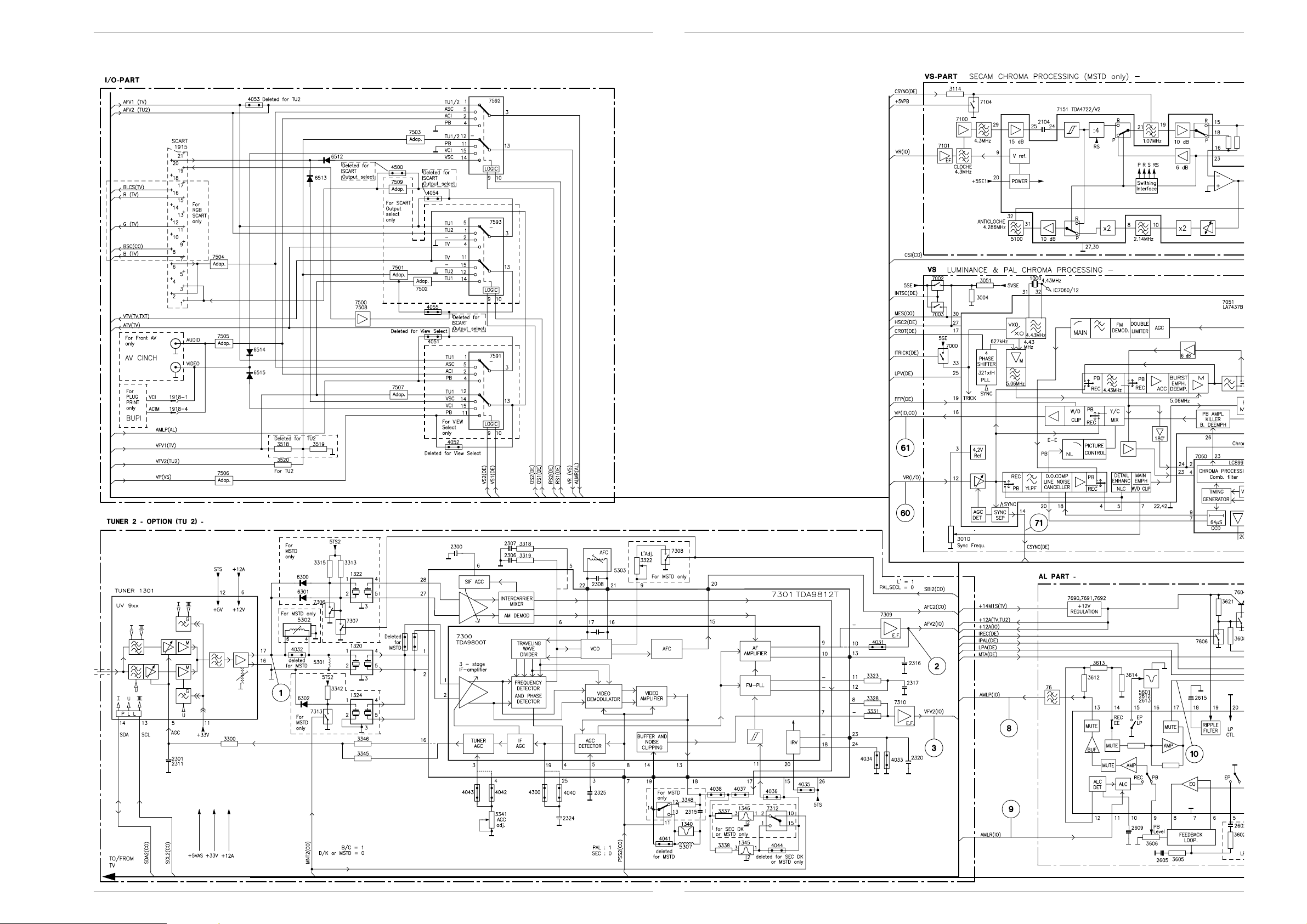
Platinenabbildungen und Schaltpläne / Layout of PCBs and Circuit Diagrams TVR 3710 …, TVR 5100 …, TVR 5500 … Platinenabbildungen und Schaltpläne / Layout of PCBs and Circuit Diagrams TVR 3710 …, TVR 5100 …, TVR 5500 …
Blockschaltplan / Block Circuit Diagram (Video-Analog)
Signal Chassis
Signal Chassis
Signal Chassis
Signal Chassis
Signal Chassis
4 - 11 GRUNDIG Service 4 - 12 GRUNDIG Service
Page 46
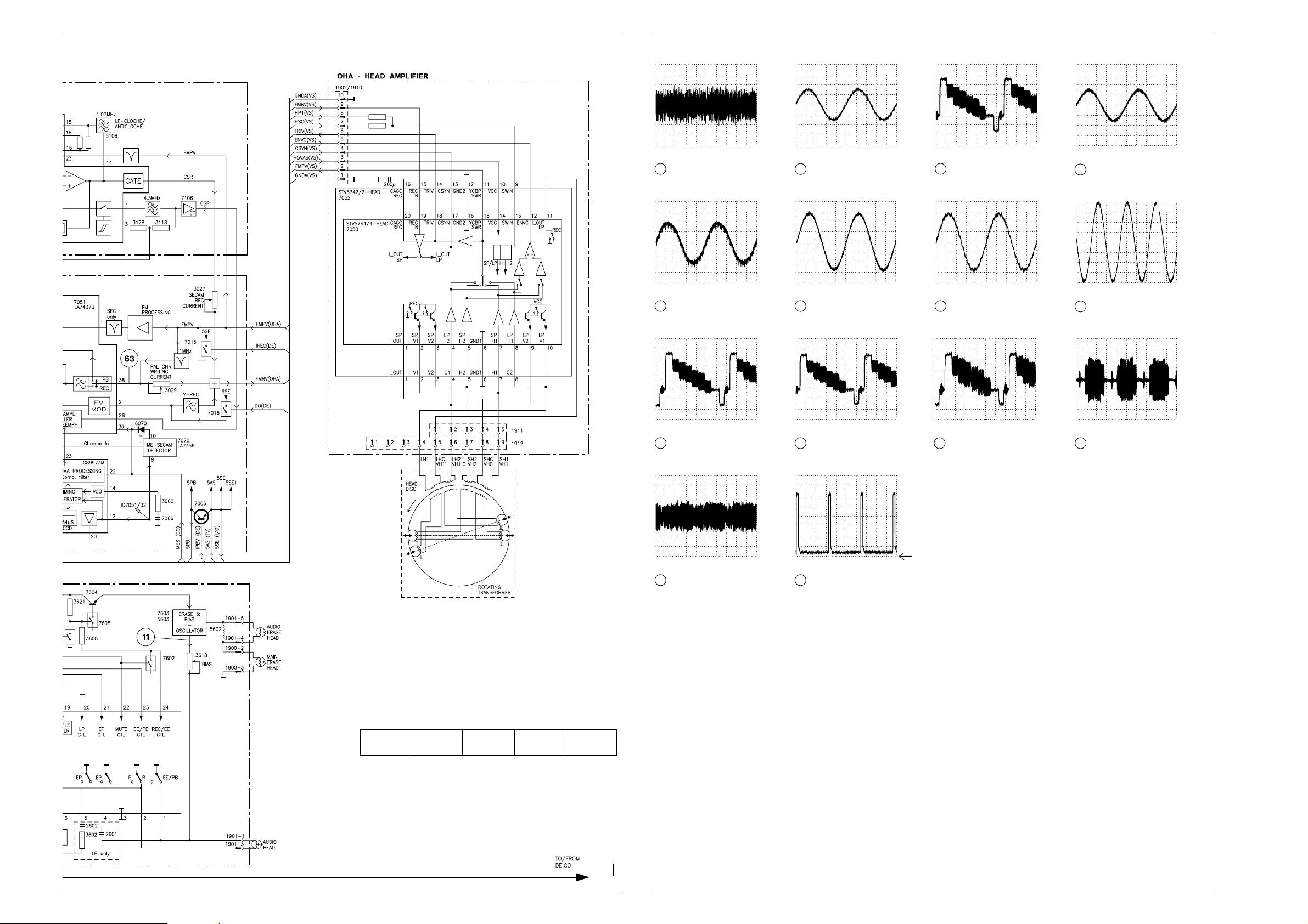
TVR 3710 …, TVR 5100 …, TVR 5500 … Platinenabbildungen und Schaltpläne / Layout of PCBs and Circuit Diagrams
AC, 200mV/Div, 10ms/Div
Tuner 1301-(17)
REC
1
AC, 200mV/Div, 200µs/Div
IC7608-(7)
PB
8
AC, 100mV/Div, 200µs/Div
IC7601-(11)
REC
9
AC, 200mV/Div, 10µs/Div
IC7051-(12)
REC
60
AC, 100mV/Div, 20µs/Div
IC7051-(38)
PB
63
TVR 3710 …, TVR 5100 …, TVR 5500 … Platinenabbildungen und Schaltpläne / Layout of PCBs and Circuit Diagrams
AC, 500mV/Div, 200µs/Div
T7309 – Collector
2
REC
REC
AC, 200mV/Div, 10µs/Div
T7310 – Emitter
3
AC, 500mV/Div, 200µs/Div
IC7601-(17)
10
REC
REC
PB
AC, 500mV/Div, 200µs/Div
IC7608-(7)
8
AC, 20V/Div, 5µs/Div
C2618
11
REC
REC
REC
7601
Reference
AL ..............P 4-65
BUPI ..........P 4-68
CO .............P 4-43
DE..............P 4-49
IO...............P 4-59
OHA...........P 4-69
PLSP .........P4-19
PSSP2.......P 4-37
TU2............P 4-55
T
ube PCB
...P 4-33
TV..............P 4-51
TXT............P 4-58
VS..............P 4-61
AC, 500mV/Div, 10µs/Div
IC7051-(16)
61
DC, 500mV/Div, 20µs/Div
IC7051-(14)
71
REC
AC, 500mV/Div, 10µs/Div
IC7051-(16)
61
0V
AC, 100mV/Div, 20µs/Div
IC7051-(38)
63
GRUNDIG Service 4 - 13
GRUNDIG Service 4 - 14
Page 47
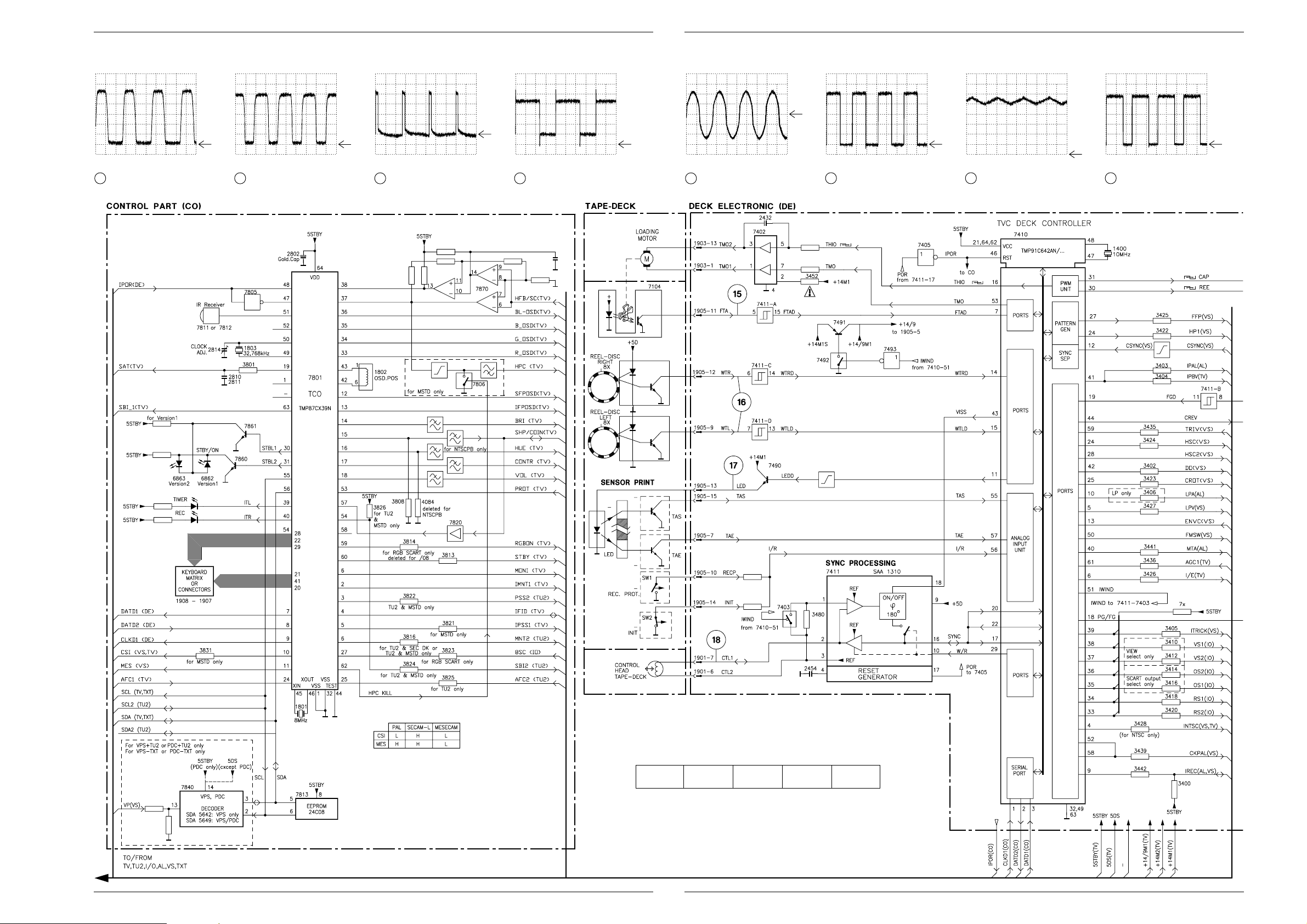
Platinenabbildungen und Schaltpläne / Layout of PCBs and Circuit Diagrams TVR 3710 …, TVR 5100 …, TVR 5500 … Platinenabbildungen und Schaltpläne / Layout of PCBs and Circuit Diagrams TVR 3710 …, TVR 5100 …, TVR 5500 …
DC, 500mV/Div, 500µs/Div
2.8V
Connector 1905-(2)
REC
19
DC, 1V/Div, 10µs/Div
0V
IC7410-(31)
REC
20
DC, 1V/Div, 10µs/Div
0V
IC7410-(30)
REC
22
Reference
AL ..............P 4-65
BUPI ..........P 4-68
CO .............P 4-43
DE..............P 4-49
IO...............P 4-59
OHA...........P 4-69
PLSP .........P 4-19
PSSP2.......P 4-37
TU2............P 4-55
T
ube PCB
...P 4-33
TV..............P 4-51
TXT............P 4-58
VS..............P 4-61
Blockschaltplan / Block Circuit Diagram (Digital)
DC, 100mV/Div, 10ms/Div
Connector 1905-(11)
15
EJECT
0V
DC, 100mV/Div, 500ms/Div
Connector 1905-(9/12), IC7411-(6/7)
16
Signal Chassis
REC
0V
DC, 100mV/Div, 5ms/Div
Connector 1905-(13)
17
REC
0V
DC, 1V/Div, 10ms/Div
Connector 1901-(7)
18
REC
0V
Signal Chassis
DC, 500mV/Div, 10µs/Div
Connector 1905-(3)
21
REC
0V
4 - 15 GRUNDIG Service 4 - 16 GRUNDIG Service
Page 48
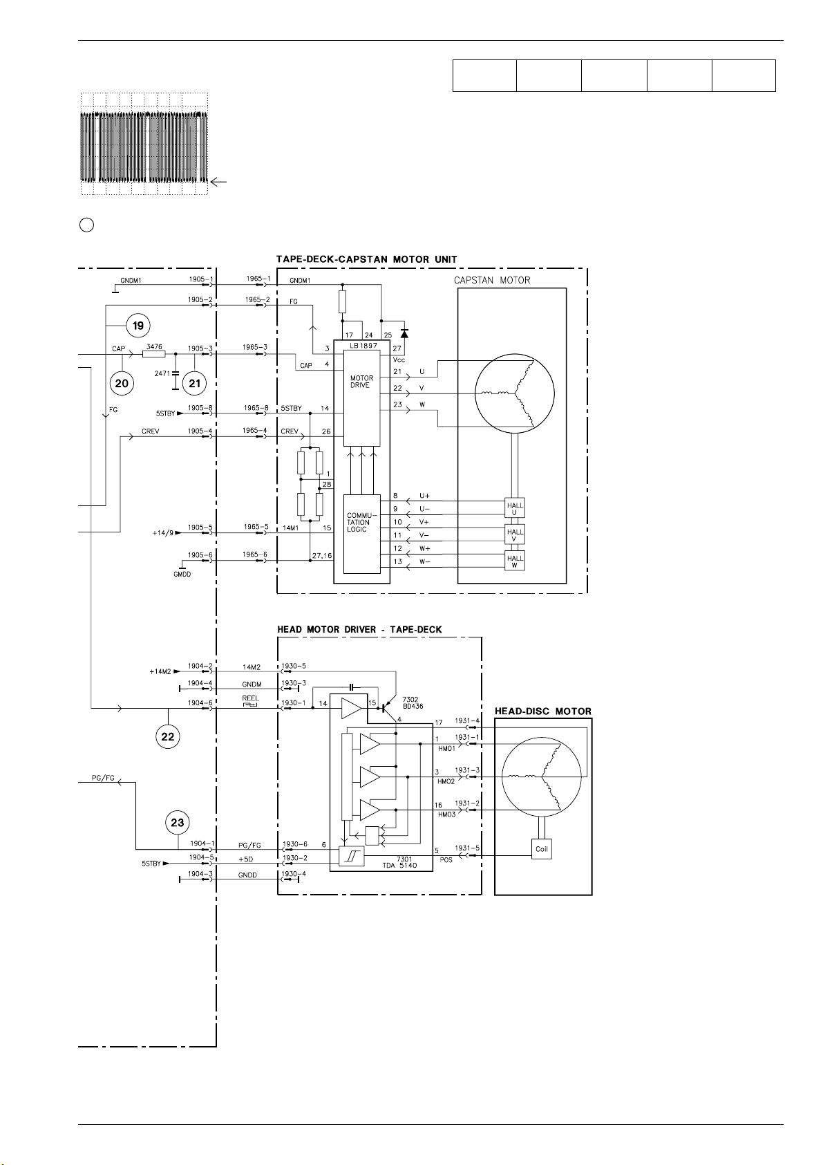
TVR 3710 …, TVR 5100 …, TVR 5500 … Platinenabbildungen und Schaltpläne / Layout of PCBs and Circuit Diagrams
REC
DC, 1V/Div, 10ms/Div
Connectors 1904-(1), 1930-(6)
23
0V
Reference
AL ..............P 4-65
BUPI ..........P 4-68
CO .............P 4-43
DE..............P 4-49
IO...............P 4-59
OHA...........P 4-69
PLSP .........P4-19
PSSP2.......P 4-37
TU2............P 4-55
T
ube PCB
...P 4-33
TV..............P 4-51
TXT............P 4-58
VS..............P 4-61
GRUNDIG Service 4 - 17
Page 49
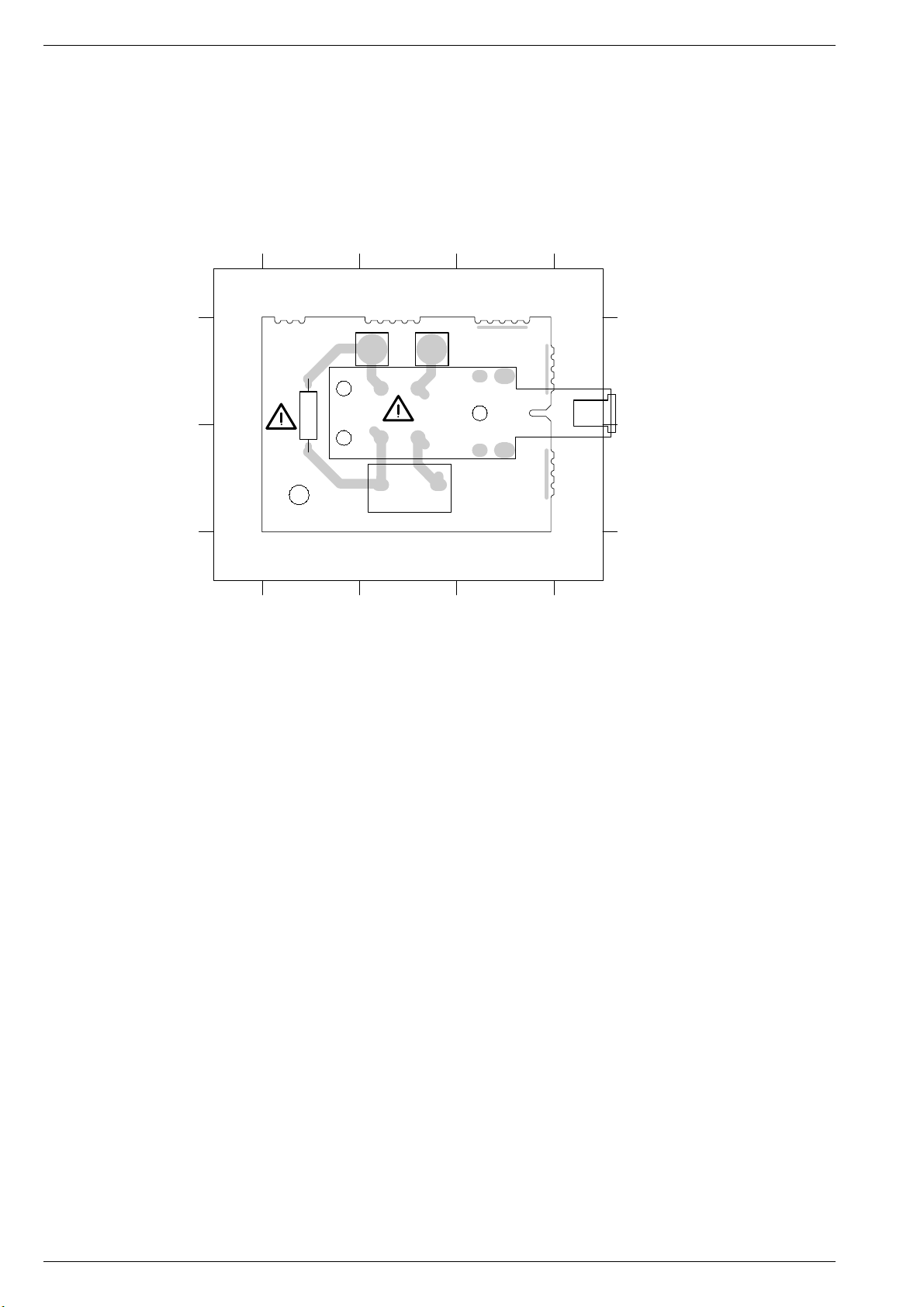
Platinenabbildungen und Schaltpläne / Layout of PCBs and Circuit Diagrams TVR 3710 …, TVR 5100 …, TVR 5500 …
Netzschalterplatte / Power Switch Board
Ansicht von der Bestückungsseite
View of Component Side
A
B
123
1013
3302
123
1003
1002
0003
1002 B 2
1003 A 3
3302 A 1
A
B
4 - 18 GRUNDIG Service
Page 50
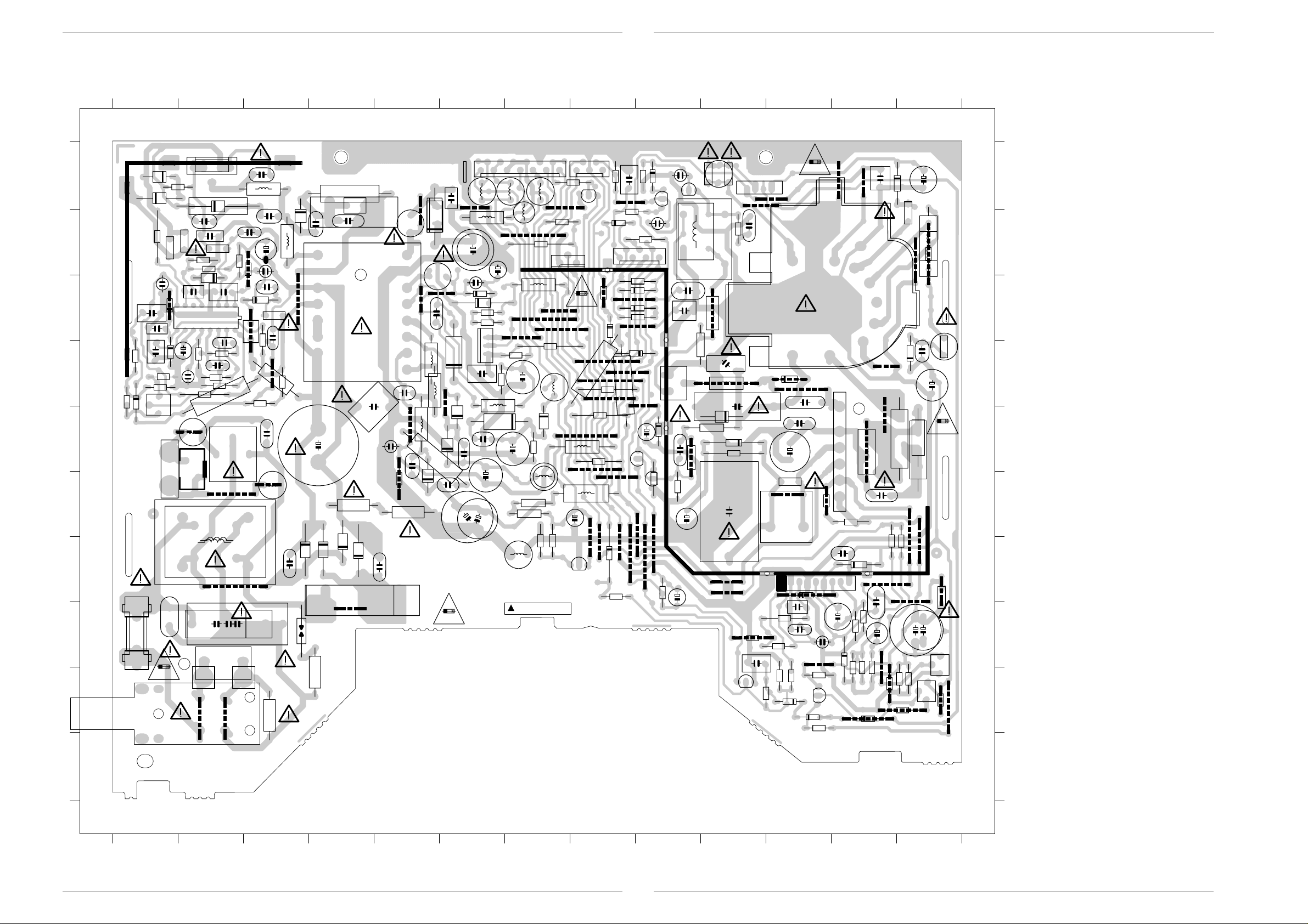
TVR 3710 …, TVR 5100 …, TVR 5500 … Platinenabbildungen und Schaltpläne / Layout of PCBs and Circuit Diagrams
TVR 3710 …, TVR 5100 …, TVR 5500 … Platinenabbildungen und Schaltpläne / Layout of PCBs and Circuit Diagrams
Leistungs-Chassis / Power Chassis (PLSP)
Ansicht von der Bestückungsseite / View of Component Side
12345678910111213
7334
7330
A
B
C
D
E
F
G
H
I
J
6336
6337
3339
6333
2333
0015
3357
6335
2337
RI SK OF FI RE
2318
2327
3356
2329
3362
9314
3359
6319
3358
3334
3322
3348
1924
6348
9318
6318
2320
3342
3363
3335
2341
3327
3330
5367
1920
5311
REPLACE FUSE AS MARKED
13110009
3309
T
1013
2. 0A 125V
1000
7310
2325
1
9311
3338
3310
9322
2313
2330
2310
2323
1001
3329
2309
9309
3333
2324
3328
3347
3311
9315
5312
9320
2311
9310
6334
9303
3324
3346
3355
2316
5350
3332
2301
5368
2334
2335
3318
2308
3341
3300
2328
2336
9323
2305
6332
5354
9326
2338
3349
1
3
3
3
6316
PLS
12345678910111213
1921, 1922, 1923 —> Signal-Chassis (1909, 1911, 1912)
1926 —> Bildrohrplatte / Tube PCB (1969)
1924, 1925 —> Bildröhre / CRT
0009 H 1
0015 A 1
0016 B 7
0050 B 8
0051 B 7
1000 I 1
1001 I 2
1013 H 2
1300 H 3
A
1311 H 1
1371 C 5
1372 B 5
1570 D 13
1571 A 10
1920 E 2
1921 A 7
1922 A 8
B
1923 B 9
1924 E 1
1925 E 12
1926 A 10
1929 A 6
2301 E 3
2305 G 3
2308 B 3
2309 B 3
C
2310 C 2
2311 H 2
2312 E 4
2313 H 2
2314 G 5
2315 E 4
2316 H 2
2318 C 1
D
2320 D 2
2323 D 2
2324 D 2
2325 D 2
2327 D 1
2328 A 3
2329 C 1
2330 B 2
E
2331 B 4
2332 B 4
2333 B 2
2334 B 3
2335 B 3
2336 C 3
2337 C 1
2338 C 3
2341 C 2
F
2351 A 6
2352 F 6
2353 D 6
2360 D 5
2361 E 5
2362 F 6
2363 F 6
2364 F 6
G
2371 C 5
2373 D 7
2374 E 7
2375 E 5
2377 C 6
2378 E 6
2379 B 6
2381 E 6
H
2382 B 6
2391 F 8
2392 B 6
2510 G 12
2511 D 13
2512 D 13
2513 H 12
2514 H 11
2515 H 11
I
2516 H 12
2517 H 11
2518 H 13
2519 H 13
2520 H 12
2551 A 12
2552 C 9
2553 G 9
J
2555 H 10
2556 E 9
2576 B 9
2580 D 11
2581 A 9
2582 C 9
2583 B 10
2584 F 10
2585 E 10
2583
3554
2588
3530
3536
5550
3558
2593
3527
9510
5510
6554
1571
1. 0A 125V
9544
2580
9571
3553
7510
9524
2517
7578
T
9529
6570
2515
2514
3579
3578
3514
9514
1925
6556
9565
2510
6524
9549
3517
2513
3556
6592
2551
9556
3592
6511
2511
9520
2592
5596
9513
9519
3538
5595
1570
3531
2512
T
3591
9521
5590
9518
2589
3519
6513
9562
2516
3512
3513
2518
2520
3559
9570
9526
3522
3518
3526
9531
6553
9516
3521
9575
3529
3589
9543
9566
3525
3590
0. 4A 125V
1570
2519
3523
3524
9515
3528
9512
3516
9569
6552
6343
3580
6550
9547
3343
9525
2594
9553
9561
1923
3582
6584
6581
3584
9572
6551
7585
3588
3581
2556
9551
9554
3599
9560
2576
6555
3555
2581
5581
9523
2586
5587
9522
6571
1571
5586
2584
9545
9541
2585
6582
3537
3585
3587
7550
5551
9517
3515
2555
1926
9563
6525
6583
9573
7586
9540
2553
3532
7584
5580
7587
2582
2552
3586
7583
3597
9527
3594
2590
3595
2587
3352
9534
9542
6373
3540
3350
9548
4. 0A 125V
8
9
35
5556
9550
5361
2391
7331
1922
0050
0051
0016
T
1371
9558
9546
9567
9530
7351
9528
9574
3551
3541
3577
3552
9552
3596
9557
1929
3345
3375
2314
9304
2360
6361
9330
6351
1371
9301
5365
5362
5363
6374
3361
2364
2362
3336
1372
9328
9305
2361
3313
1372
3340
3314
5330
5331
2331
2332
HOT PART
2312
2315
6313
6315
3337
9307
3312
2375
HOT PART
6314
5371
2351
5351
6353
2379
2377
9302
6393
2371
3360
7352
6371
9312
2353
6375
2381
2378
2
T
2382
3371
5370
6372
2352
3
36
1921
5372
2392
6392
3364
9533
2374
3391
3393
5366
UL- Kennung
5353
5352
9555
3351
5364
3354
2373
5375
3395
7350
9564
3353
5373
3372
5374
3394
4. 0A 125V
1300
3304
6614. L4
PLS- U
6371. 4
2586 D 10
2587 F 9
2588 E 11
2589 F 12
2590 E 9
2592 A 13
2593 E 11
2594 A 8
3300 I 3
3304 I 4
3309 H 1
3310 E 2
3311 E 2
3312 F 4
3313 F 5
3314 A 4
3318 C 3
3322 B 2
3324 D 2
3327 D 2
3328 D 2
3329 A 2
3330 D 2
3331 D 3
3332 C 3
3333 B 2
3334 B 1
3335 B 2
3336 B 4
3337 G 4
3338 B 2
3339 A 2
3340 G 4
3341 C 3
3342 D 2
3343 G 8
3345 A 4
3346 B 3
3347 E 2
3348 B 2
3349 D 3
3350 A 8
3351 B 7
3352 B 7
3353 D 7
3354 D 7
3355 D 3
3356 D 1
3357 D 1
3358 D 1
3359 B 1
3360 C 6
3361 E 6
3362 D 1
3363 D 1
3364 C 6
3371 D 6
3372 E 7
3375 F 5
3391 F 7
3393 F 7
3394 G 7
3395 G 7
3512 H 12
3513 H 12
3514 F 11
3515 H 10
3516 G 13
3517 F 12
3518 I 12
3519 G 12
3521 G 13
3522 I 12
3523 H 13
3524 I 13
3525 I 13
3526 I 12
3527 F 11
3528 I 13
3529 I 13
3530 H 11
3531 D 13
3532 A 10
3536 H 11
3537 A 10
3538 B 13
3540 E 8
3541 E 8
3551 D 8
3552 C 8
3553 I 11
3554 I 11
3555 G 9
3556 I 12
3558 I 11
3559 I 13
3577 B 8
3578 I 11
3579 I 11
3580 A 8
3581 B 9
3582 C 9
3584 C 9
3585 B 10
3586 D 10
3587 E 10
3588 A 9
3589 E 13
3590 E 13
3591 E 13
3592 B 13
3594 E 9
3595 F 9
3596 D 9
3597 E 10
3598 C 9
3599 F 9
5311 G 2
5312 G 2
5330 C 4
5331 C 4
5350 A 3
5351 B 6
5352 B 7
5353 A 7
5354 B 3
5361 F 8
5362 D 5
5363 E 5
5364 C 7
5365 D 5
5366 G 7
5367 E 2
5368 F 3
5370 E 6
5371 A 6
5372 A 7
5373 D 7
5374 F 7
5375 F 7
5510 F 11
5550 C 11
5551 C 11
5556 E 8
5580 B 9
5581 B 10
5586 C 10
5587 D 10
5590 E 12
5595 B 13
5596 B 13
6313 G 4
6314 G 4
6315 G 4
6316 G 3
6318 C 1
6319 D 1
6332 B 3
6333 A 2
6334 C 3
6335 D 1
6336 A 1
6337 A 1
6343 G 8
6348 C 2
6351 B 5
6353 B 5
6361 F 5
6371 D 6
6372 E 6
6373 E 7
6374 E 6
6375 E 6
6392 C 6
6393 C 6
6511 D 13
6513 G 12
6524 H 12
6525 G 11
6550 B 8
6551 D 9
6552 C 8
6553 I 12
6554 I 11
6555 E 9
6556 I 11
6570 D 11
6571 E 10
6581 C 9
6582 E 10
6583 A 9
6584 C 9
6592 A 13
7310 C 2
7330 A 2
7331 G 8
7334 A 2
7350 B 7
7351 A 8
7352 D 6
7510 G 11
7550 I 10
7578 I 11
7583 D 9
7584 A 9
7585 E 9
7586 F 9
7587 A 9
9301 C 5
9302 C 6
9303 C 3
9304 B 5
9305 F 5
9307 H 4
9309 B 3
9310 I 2
9311 I 2
9312 D 6
9314 E 2
9315 F 3
9318 C 1
9320 G 2
9322 F 2
9323 D 3
9326 C 3
9328 E 5
9330 A 6
9510 F 11
9512 G 13
9513 B 13
9514 F 11
9515 I 13
9516 I 13
9517 H 10
9518 E 12
9519 B 13
9520 D 12
9521 E 12
9522 D 10
9523 C 10
9524 G 11
9525 G 8
9526 I 12
9527 E 9
9528 C 8
9529 D 11
9530 G 8
9531 I 12
9533 C 7
9534 C 7
9540 G 9
9541 G 10
9542 C 7
9543 F 13
9544 A 11
9545 G 10
9546 D 8
9547 F 8
9548 A 7
9549 A 12
9550 E 8
9551 F 9
9552 D 8
9553 A 8
9554 E 9
9555 B 7
9556 A 12
9557 G 8
9558 D 8
9560 G 9
9561 G 8
9562 G 12
9563 A 10
9564 C 7
9565 D 11
9566 G 13
9567 E 8
9569 I 13
9570 I 12
9571 H 11
9572 C 9
9573 C 8
9574 D 8
9575 H 13
GRUNDIG Service 4 - 19
GRUNDIG Service 4 - 20
Page 51
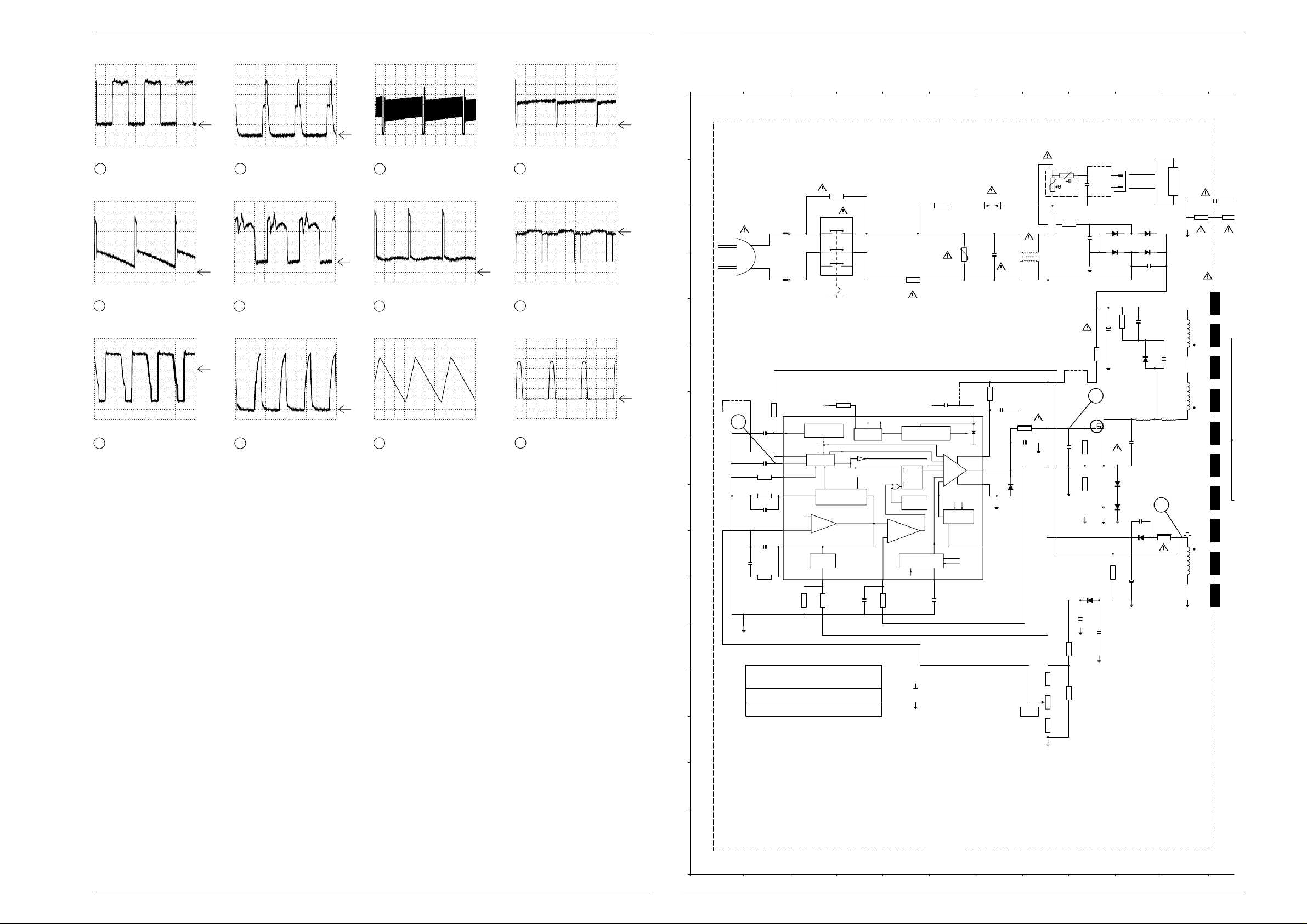
Platinenabbildungen und Schaltpläne / Layout of PCBs and Circuit Diagrams TVR 3710 …, TVR 5100 …, TVR 5500 … Platinenabbildungen und Schaltpläne / Layout of PCBs and Circuit Diagrams TVR 3710 …, TVR 5100 …, TVR 5500 …
Leistungs-Chassis / Power Chassis TVR 3710 … (PLSP)
TV
TV
TV
TV
4561 7 8 9 10 11 1223
DC, 500mV/Div, 20µs/Div
IC7200-(37), Connector 1922-(4)
33
TV
DC, 10V/Div, 5ms/Div
IC7510-(5)
46
PB
DC, 10V/Div, 5µs/Div
Trafo 5330-(4), 5331-(4)
50
0V
DC, 1V/Div, 20µs/Div
IC7200-(38), Connector 1922-(5)
34
0V
DC, 200mV/Div, 20µs/Div
T7584 – Basis
47
0V
DC, 2V/Div, 5µs/Div
T7330 – Gate
51
TV
PB
0V
AC, 1V/Div, 5ms/Div
IC7200-(43), Connector 1922-(1)
43
0V
DC, 5V/Div, 5ms/Div
IC7510-(8)
48
0V
AC, 500mV/Div, 10µs/Div
IC7310-(10)
52
TV
STANDBY
DC, 1V/Div, 5ms/Div
IC7510-(1)
45
0V
DC, 5V/Div, 20µs/Div
T7583 – Basis
49
DC, 200V/Div, 20µs/Div
T7583, Collector
53
TV
TV
0V
0V
0V
A
B
C
D
E
F
G
H
I
J
K
L
9318
52
1301
2323
4n7
2324
2329
2327
470p
3328
3327
6k8
2325
560p
3324
82p
33k
100k
2,5V
1n
3342
0,3V
2,6V
2,6V
0,3V
2,3V
56k
8
9
10
15
12
14
13
3300
4M7
1000
1
2
IN
23
1
DEMAGNETICATION
Vdem in
MANAGEMENT
Vdem out
Iref
Sync
C
OSCILLATOR
T
R standby
F
R standby
P
2.5V
VOLTAGE
FEEDBACK
E/A OUT
FOLDBACK INPUT
(REDUCED FREQUENCY)
ERROR
AMP
FOLDBACK
5
1,3V
18k
3322
3348
STANDBY
180k
4
OUT VDR
1311
T2,5AH
3330
10k
Vosc
CURRENT SENSE INPUT
MC44603P
2,5V
16 1
Rref
Vref
Iref
REFERENCE
BLOCK
Vosc prot
Iref
2n2
2341
3359
Vref
enable
CURRENT
SENSE
7
330E
7310
SUPPLY &
INITIALIZATION BLOCK
Q
Set
Latch
Reset
THERMAL
SHUTDOWN
Dmax & SOFT-START
CONTROL
Iref
2,4V
3304
270E
2310
100n
UVLO1
BUFFER
Vovp out
Vref
OVERVOLTAGE
MANAGEMENT
OVERVOLTAGE
PROTECTION
UVLO1
Vref
Soft Start & Dmax
11
2u2
2320
3309
9309
13,5V
Vcc
Vcc
1300
SIQV-S10K300
3333
18V
Vc
2
3
OUTPUT
4
GND
6
2311
13V
2,3V
3310
3337
2330
3356
9314
1924
1
3
2n2
2301
9315
2E
2n2
2314
290V
3331
9303
2315
270k
2
6314
1N5062
6313
1N5062
68u
Degaussing Coil
24k
3345
2331
6315
1N5062
6316
1N5062
2305
2n2
10n
6332
BYT54
2332
470p
2312
1n
3312
3313
3M9
3M9
5331
7
6
5
51
50
3341
5E6
5354
80E
1
2
8
4
3
7330
2,2V
4n7
3339
3334
BAV21
6335
100n
2337
11k
1k
0E47
STP4NA60FI
4n7
2338
3347
6336
6337
100E
329V
BYT54
BYT54
2328
2335
5350
80E
220p
2336
220p
6334
BYD33D
100u
2
1
5311
470n
DMF-2830
68E
2308
1n
3338
39E
2309
4n7
6348
BYV10-20
HOT CIRCUIT , BE CAREFUL AND USE AN
20k
Ubat
3357
3358
3362
5k9
3363
4k7
20k
M
ISOLATION TRANSFORMER WHEN SERVICING
DO NOT OPERATE WITHOUT CASE
CAUTION : LETHAL POTENTIALS AT PRIMARY
COLD GND
HOT GND
N
BECAUSE A HOT GROUND IS PRESENT IN THE POWER SUPPLY CIRCUIT, AN ISOLATION
O
TRANSFORMER MUST BE USED. ALSO, IN ORDER TO HAVE THE ABILITY TO INCREASE
THE INPUT VOLTAGE SLOWLY, WHEN TROUBLESHOOTING THIS TYPE OF POWER SUPPLY
CIRCUIT, A VARIABLE ISOLATION TRANSFORMER IS REQUIRED.
P
HOT PART
4561 7 8 9 10 11 1223
4 - 21 GRUNDIG Service 4 - 22 GRUNDIG Service
Page 52
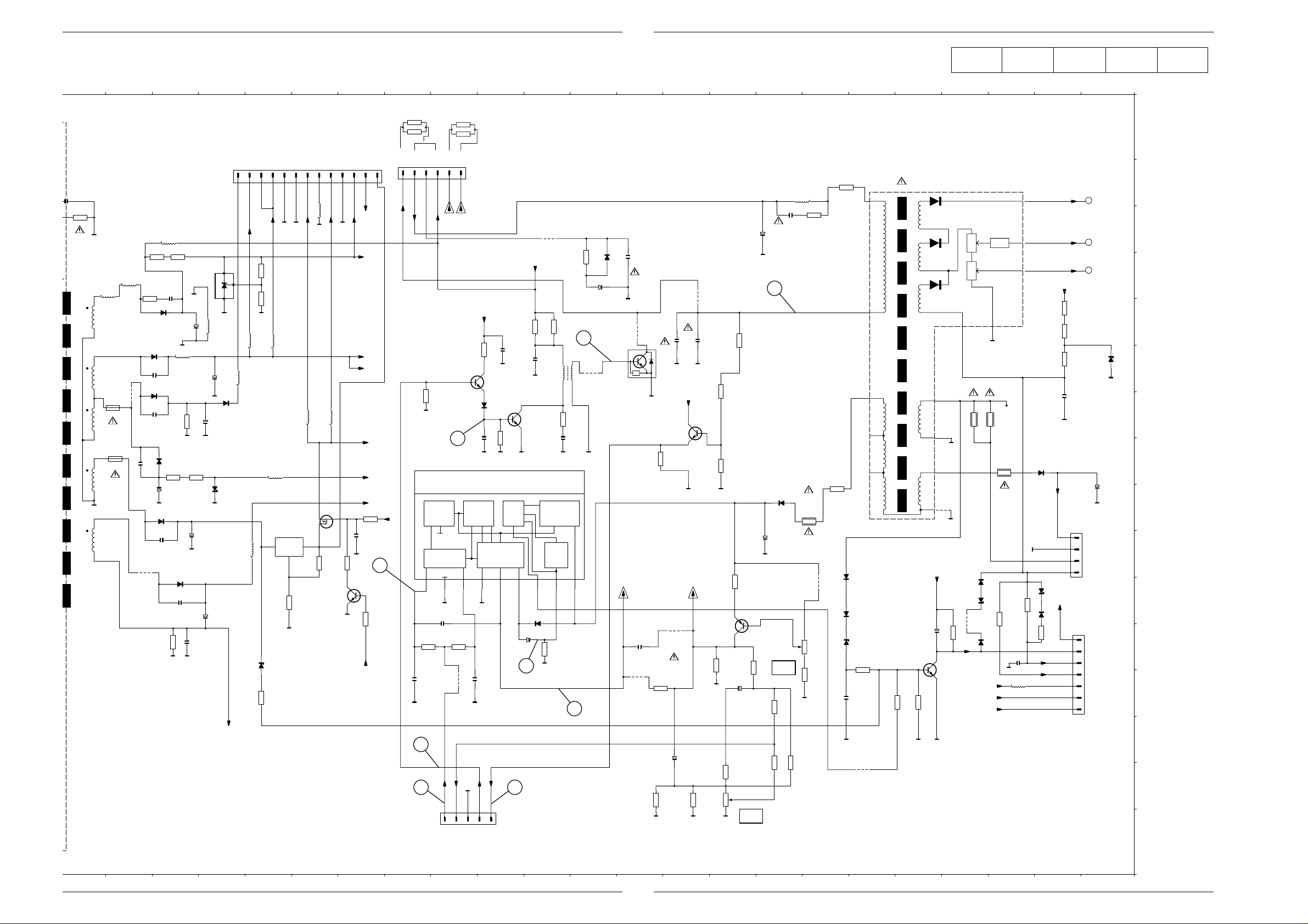
TVR 3710 …, TVR 5100 …, TVR 5500 … Platinenabbildungen und Schaltpläne / Layout of PCBs and Circuit Diagrams
Reference
AL ..............P 4-65
BUPI ..........P 4-68
CO .............P 4-43
DE..............P 4-49
IO...............P 4-59
OHA...........P 4-69
PLSP .........P4-19
PSSP2.......P 4-37
TU2............P 4-55
T
ube PCB
...P 4-33
TV..............P 4-51
TXT............P 4-58
VS..............P 4-61
TVR 3710 …, TVR 5100 …, TVR 5500 … Platinenabbildungen und Schaltpläne / Layout of PCBs and Circuit Diagrams
2312
1n
3313
3M9
32 33 3412 13 14 15 16 17 18 19 20 21 22 23 24 25 26 27 28 29 30 31
DEFLECTIONVERTICALHORIZONTAL
to Signal Chassis (TV) 1909
33A
5A
22u
7350
4,1V
GNDM
LM317T
3351
6
1
GNDM
7352
MTP3055E
2k7
5D
789
5351
22u
5352
5,29V
3352
GND5D
80E
5,1V
820E
22u
5353
7351
BC548B
GND5A
10
14,2V
3353
STBY
111213
STBY
33A
14H
14H
3354
220k
100n
2353
1k
43mV
3350
STBY
5Stby
HDEF1
1925
1
5D1
-7V
9A
14H
45
10k
Ubat
Ubatlot
HDEF2
VDEFH
VDEFL
2
3
4
5
6
VDEFH
VDEFL
8
8V
680E
100n
2594
3577
4,8V
1,4V
7587
BC548B
4k7
3580
Thermal
Protection
Driver
GND
2,2V
23
1
0V 2,2V 15,5V0V 28,6V 1,8V 6,3V 28,3V
2514
390p
3536
4k7
2n2
2515
0,95V
BAV21
6583
0,47V
47
3530
3k3
330p
2581
3588
150E
TDA3653C/N2
9517
Output
Stage
Protection
2517
Guard
Circuit
Output Stage
45678
2n2
82,7V
17,2V
7584
MPSA43
2513
100u
48
Ubat
3596
2552
7510
BAV21
9510
10k
100n
Voltage Stab.
Current Source
Generator
6513
3513
3598
Flyback
1k2
&
5580
3585
2583
10k
2k2
1n
9
46
CU10
49
3587
9523
10k
2587
2u2
6582
BYD33D
7583
BU1508DX
2584
VDEFH
9514
560n
9522
2516
100n
3555
8911
3537
9528
4k7
4E7
6551
6552
6550
5550
focus
screen
3532
BAV21
BZX79-C18
BAV21
GNDAU
9A
-7V
ANODE TO CRT
TO TUBE PCB/1991
FOCUS
TO TUBE PCB/1993
SCREEN
Ubat
12k
BYD33J
6592
6584
56k
6581
3584
3540
3541
3551
2551
BZX79-C10
8
BAV21
22k
12k
39k
33n
1926
1
2
3
4
1923
1
2
3
4
5
6
7
2592
VRGB
GNDA
HEATER
AQUADAG
8
PROT
BCI
VCOMP
GND9A
9A
-7V
6555
4u7
G
4E7
3592
4E7
3582
3581
3M3
2582
220n
5556
80E
3591
4E7
2
2593
5590
47u
3590
2589
39E
10n
47u
53
9529
8n2
1n5
2586
1k
9512
5,2V
7585
BC548B
2585
5D1
1,1V
VDEFL
3579
86V
0,96V
3599
3517
470E
3594
3595
BC558B
150k
3597
150k
15k
3538
3518
BYD33D
6511
470u
2512
v-shift
1k2
5k1
3519
28,3V
3578
270E
7578
1k2
2520
100u
3529
2E7
3531
4E7
9515
3524
4k7
10k
6553
6556
6554
2555
BAV21
BAV21
BZX79-C24
3554
2k2
100n
1
6
5
4
3553
10
7
3
9520
5D1
10u
2553
4,9V
14mV
7550
BC548B
68k
22k
3558
14M2
14M1
14/9M1
1921
1
5361
33u
3391
3393
5k6
4k7
5363
80E
3361
5365
80E
12
15
13
14
15
16
15
11
10
9302
1371
T2,5A
1372
T2,5A
9
39E
BYW98-200
BYW98-200
1n5
2377
9312
6361
BYW36
6371
2371
470p
6372
2381
470p
BAV21
2392
6351
BYW98-200
2351
470p
2364
470p
5370
80E
3372
6392
3360
390E
10u
6374
BYT54
2378
1n
2375
3375
180E
2379
390E
3364
1n
2363
1k
TL431CLP
560u
47u
2374
2352
7331
5366
22u
2373
680u
6393
680u
32V
K
A
680u
6373
BYV10-20
BZX85-C6V8
GNDAU
R
5373
14M2
2
345
3394
100k
2,45V
8k2
3395
22u
5371
5372
22u
5364
80E
23
22u
5374
8,5V
6343
BZX79-C9V1
10k
3343
33
2519
43
3
1
1922
VDR
to Signal Chassis (TV) 1911
4
2
VFB
HDR
GNDTV
5
HFB/SC
34
3559
1000u
22E
3522
2E7
3525
4E7
3523
100E
v-amp
3521
10k
390E
3556
9524
1000 C 3
1300 B 7
1311 D 5
1371 G13
1372 H13
1921 B15
A
1922 P20
1923 L33
1924 B 9
1925 B19
1926 J33
2301 B 9
2305 D10
2308 G 7
2309 H 8
2310 G 6
B
2312 B12
2313 D 7
2314 C 9
2315 E 9
2320 K 6
2323 J 2
2324 J 2
2325 I 2
C
2327 H 2
2328 H10
2329 G 2
2330 H 8
2331 E10
2332 F10
2335 K10
2336 I10
2337 K 9
D
2338 L 9
2341 K 4
2351 J14
2352 K15
2353 J18
2363 E14
2364 D14
2371 F14
E
2373 F15
2374 G15
2375 L14
2377 H13
2378 K14
2379 J14
2381 G14
2392 I14
BZX79-B30
2512 J27
F
2513 L22
2514 K20
2515 M19
2516 L24
2517 M20
2519 N25
2520 M26
2551 G33
G
2552 F22
2553 L30
2555 M28
2581 G21
2582 L32
2583 G22
2584 D24
2585 E25
2586 E25
H
2587 D23
2589 C27
2592 I34
2593 C27
2594 F21
3300 B 4
3304 B 6
3309 D 6
I
3310 B 8
3312 C11
3313 C12
3322 K 3
3324 J 2
3327 I 2
3328 H 2
3330 G 4
J
3331 F 9
3333 G 7
3334 H 9
3337 C 9
3338 G 8
3339 H 9
3341 J11
3342 G 2
3343 M16
K
3345 E10
3347 J 9
3348 K 3
3350 K18
3351 K16
3352 J17
3353 J18
3354 I18
L
3356 L 8
3357 M 8
3358 M 8
3359 K 4
3360 H14
3361 D13
3362 N 8
3363 M 8
3364 H14
M
3372 G14
3375 L14
3391 D14
to Signal Chassis (TV) 1912 to TUBE PCB 1969
3393 D14
3394 D16
3395 D16
3513 L22
3517 M24
N
3518 L26
3519 M27
3521 N27
3522 O26
3523 O26
3524 L28
3525 O25
3529 M27
O
3530 L20
3531 I28
3532 G31
3536 L19
3537 G31
3538 H28
3540 E33
3541 E33
3551 F33
3553 M29
3554 L29
P
3555 L31
3556 O27
3558 M30
3559 O24
3577 F21
3578 K26
3579 L26
3580 G19
3581 K32
3582 K32
3584 L33
3585 G22
3587 D23
3588 G21
3590 C28
3591 B28
3592 H32
3594 F26
3595 H26
3596 E22
3597 E26
3598 E22
3599 H24
5311 C 8
5331 D11
5350 G10
5351 C17
5352 G17
5353 G17
5354 G11
5361 C14
5363 D13
5364 H16
5365 D13
5366 E15
5370 F14
5371 E16
5372 E16
5373 F15
5374 J16
5550 B31
5556 M32
5580 F22
5590 B27
6313 C 9
6314 C 9
6315 C10
6316 C10
6332 F10
6334 J10
6335 K 9
6336 H 9
6337 I 9
6343 L16
6348 I 7
6351 I14
6361 E14
6371 F14
6372 G14
6373 G15
6374 K14
6392 H14
6393 I15
6511 I27
6513 K22
6550 L31
6551 K31
6552 K31
6553 K28
6554 L28
6555 F34
6556 K28
6581 K32
6582 D23
6583 G21
6584 K32
6592 H33
7310 G 5
7330 G 9
7331 D15
7350 J16
7351 K18
7352 I17
7510 H22
7550 L30
7578 L26
7583 E23
7584 G21
7585 G25
7587 F21
9302 G13
9303 F 9
9309 G 6
9312 J13
9314 B 9
9315 B 9
9318 G 1
9510 C22
9512 L25
9514 M24
9515 K28
9517 M20
9520 I30
9522 E24
9523 F23
9524 O29
9528 K31
9529 D25
32 33 3412 13 14 15 16 17 18 19 20 21 22 23 24 25 26 27 28 29 30 31
GRUNDIG Service 4 - 23
GRUNDIG Service 4 - 24
Page 53
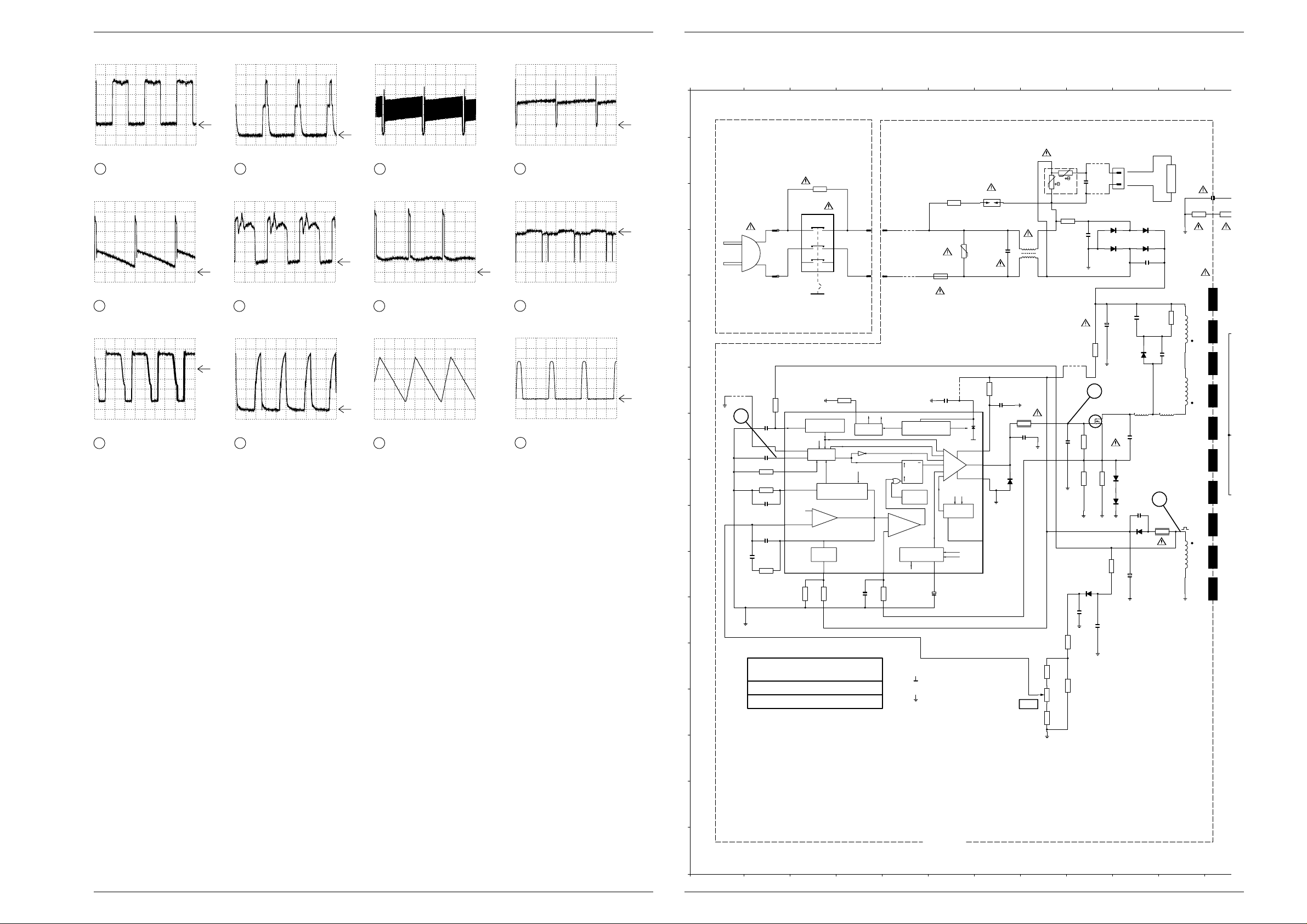
Platinenabbildungen und Schaltpläne / Layout of PCBs and Circuit Diagrams TVR 3710 …, TVR 5100 …, TVR 5500 … Platinenabbildungen und Schaltpläne / Layout of PCBs and Circuit Diagrams TVR 3710 …, TVR 5100 …, TVR 5500 …
50
51
2,4V
1,3V
2,3V
2,5V
0,3V
2,6V
2,6V
0,3V
2,5V
13,5V
13V
2,3V
2,2V
329V
290V
BECAUSE A HOT GROUND IS PRESENT IN THE POWER SUPPLY CIRCUIT, AN ISOLATION
TRANSFORMER MUST BE USED. ALSO, IN ORDER TO HAVE THE ABILITY TO INCREASE
THE INPUT VOLTAGE SLOWLY, WHEN TROUBLESHOOTING THIS TYPE OF POWER SUPPLY
CIRCUIT, A VARIABLE ISOLATION TRANSFORMER IS REQUIRED.
HOT GND
COLD GND
Degaussing Coil
VDR
HOT PART
SWITCH PCB
Ubat
4561 7 8 9 10 11 1223
N
M
Q
L
K
J
I
H
G
F
E
D
C
P
B
A
O
4561 7 8 9 10 11 1223
5k9
3363
20k
3362
3313
3M9
270k
3331
3336
24k
330E
3359
180k
3348
56k
3342
33k
3328
0E82
3335
1k
3339
5k1
3327
10k
3330
100k
3324
18k
3322
3304
270E
10k
3356
20k
3357
0E82
3334
3337
2E
68E
3333
3312
3M9
100E
3347
9309
9303
9310
9311
9314
9315
9318
39E
3338
5E6
3341
5350
80E
5354
80E
220n
2316
2309
4n7
2308
1n
2n2
2301
220p
2336
4n7
2330
470p
2332
2331
10n
1n
2324
2310
100n
2329
82p
470p
2327
2341
2n2
2n2
2314
2n2
2305
470p
2328
4n7
2338
100n
2337
2323
4n7
1n
2312
2325
560p
BYV10-20
6348
BYT54
6332
BYD33D
6334
BAV21
6335
1N5062
6315
1N5062
6313
1N5062
6314
1N5062
6316
BYT54
6336
BYT54
6337
2u2
2320
68u
2315
100u
2335
5330
1
3
4
5
6
7
2
8
STP4NA60FI
7330
DMF-2830
5311
1300
T2,5AH
1311
3310
1
2
3
1013
1013
1924
1
2
4k7
3358
SIQV-S10K300
3309
7310MC44603P
10
11
12
13
14
15
16 1
2
3
4
5
6
7
8
9
(REDUCED FREQUENCY)
AMP
ERROR
FOLDBACK
MANAGEMENT
OSCILLATOR
Iref
DEMAGNETICATION
Vdem out
STANDBY
2.5V
P
F
T
FOLDBACK INPUT
E/A OUT
R standby
Sync
R standby
VOLTAGE
C
FEEDBACK
Vdem in
CURRENT SENSE INPUT
Vosc
REFERENCE
Vref
BLOCK
Iref
enable
Vref
CURRENT
SENSE
Vosc prot
Iref
Dmax & SOFT-START
INITIALIZATION BLOCK
Set
Latch
Reset
SHUTDOWN
THERMAL
CONTROL
SUPPLY &
Q
Rref
Soft Start & Dmax
Iref
Vovp out
Vref
BUFFER
OVERVOLTAGE
MANAGEMENT
UVLO1
Vref
OVERVOLTAGE
PROTECTION
UVLO1
Vcc
Vcc
OUTPUT
GND
18V
Vc
CAUTION : LETHAL POTENTIALS AT PRIMARY
DO NOT OPERATE WITHOUT CASE
ISOLATION TRANSFORMER WHEN SERVICING
HOT CIRCUIT , BE CAREFUL AND USE AN
52
1301
IN OUT
1013
1013
1003
1
23
4
2
1
3302
4M7
Leistungs-Chassis / Power Chassis TVR 5100 … (PLSP)
TV
TV
TV
TV
DC, 500mV/Div, 20µs/Div
IC7200-(37), Connector 1922-(4)
33
DC, 10V/Div, 5ms/Div
IC7510-(5)
46
DC, 10V/Div, 5µs/Div
Trafo 5330-(4), 5331-(4)
50
0V
DC, 1V/Div, 20µs/Div
IC7200-(38), Connector 1922-(5)
34
TV
0V
DC, 200mV/Div, 20µs/Div
T7584 – Basis
47
PB
0V
DC, 2V/Div, 5µs/Div
T7330 – Gate
51
0V
0V
AC, 1V/Div, 5ms/Div
IC7200-(43), Connector 1922-(1)
43
TV
STANDBY
TV
0V
DC, 5V/Div, 5ms/Div
IC7510-(8)
48
PB
0V
AC, 500mV/Div, 10µs/Div
IC7310-(10)
52
DC, 1V/Div, 5ms/Div
IC7510-(1)
45
0V
DC, 5V/Div, 20µs/Div
T7583 – Basis
49
DC, 200V/Div, 20µs/Div
T7583, Collector
53
TV
0V
TV
0V
4 - 25 GRUNDIG Service 4 - 26 GRUNDIG Service
Page 54
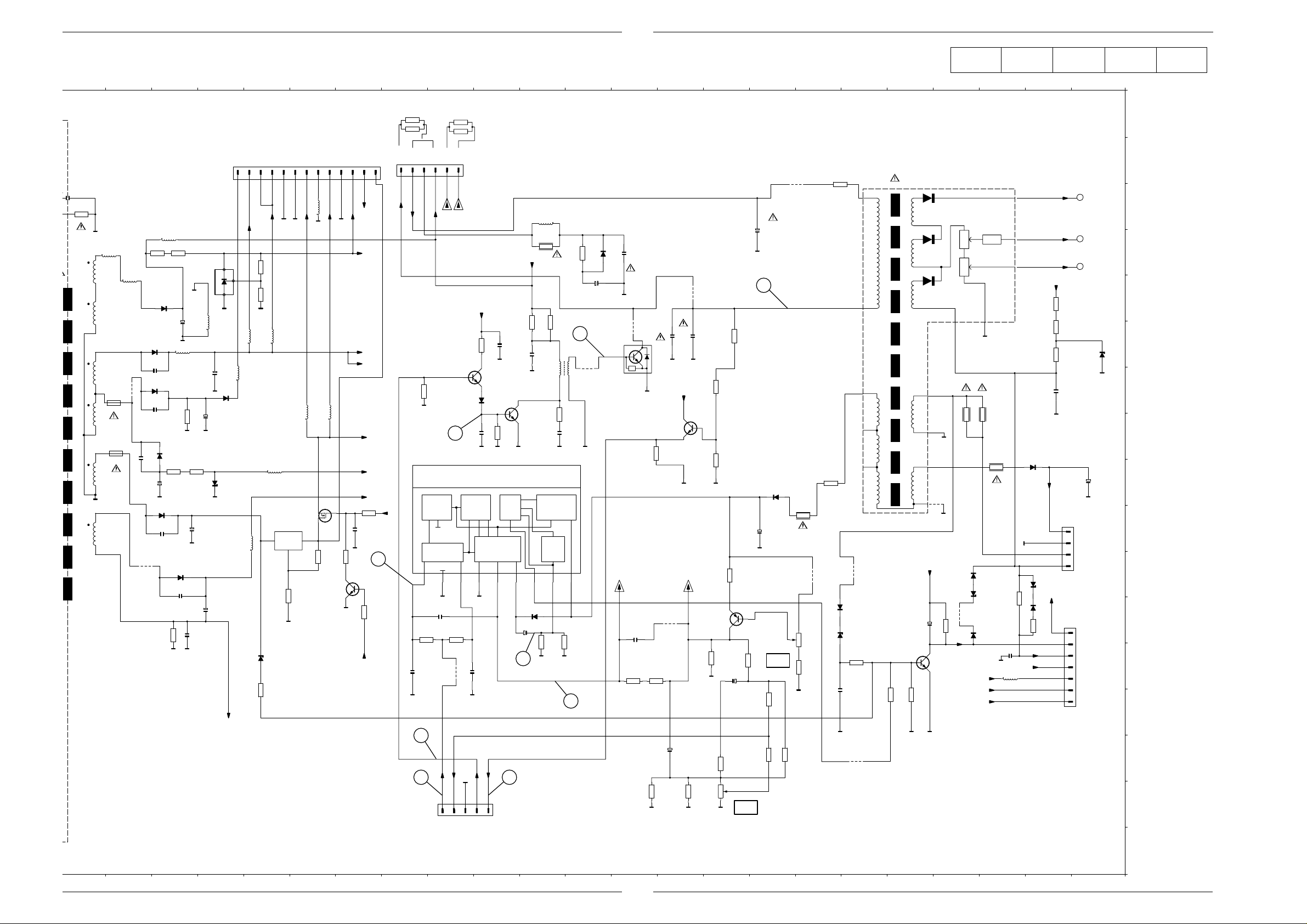
TVR 3710 …, TVR 5100 …, TVR 5500 … Platinenabbildungen und Schaltpläne / Layout of PCBs and Circuit Diagrams
Reference
AL ..............P 4-65
BUPI ..........P 4-68
CO .............P 4-43
DE..............P 4-49
IO...............P 4-59
OHA...........P 4-69
PLSP .........P4-19
PSSP2.......P 4-37
TU2............P 4-55
T
ube PCB
...P 4-33
TV..............P 4-51
TXT............P 4-58
VS..............P 4-61
TVR 3710 …, TVR 5100 …, TVR 5500 … Platinenabbildungen und Schaltpläne / Layout of PCBs and Circuit Diagrams
2312
1n
3313
3M9
32 33 3412 13 14 15 16 17 18 19 20 21 22 23 24 25 26 27 28 29 30 31
HORIZONTAL VERTICAL DEFLECTION
to Signal Chassis (TV) 1909
80E
820E
5A
5353
BC548B
22u
7351
GND5A
10
14,2V
3353
33A
STBY
111213
STBY
33A
14H
14H
-7V
3354
220k
100n
2353
1k
43mV
3350
STBY
5Stby
HDEF1
Ubatlot
HDEF2
1925
1
2
3
3580
5D1
9A
14H
Protection
45
2,2V
1
10k
3536
5k6
2n2
2515
VDEFH
Ubat
456
VDEFH
4k7
Thermal
Driver
GND
23
2514
1n
VDEFL
VDEFL
8
8V
680E
100n
2594
3577
4,8V
1,4V
7587
BC548B
0,95V
BAV21
6583
0,47V
47
3530
1k8
9517
330p
2581
3588
150E
TDA3653C/N2
Output
Stage
Protection
2517
Guard
Circuit
Output Stage
45678
10n
82,7V
17,2V
7584
MPSA43
2513
100u
48
Ubat
3596
2552
7510
6513
BAV21
5510
20u
3527
1k
12k
3598
100n
Voltage Stab.
&
Current Source
Flyback
Generator
3513
680E
12k
3585
2583
28,3V6,3V1,8V28,6V0V 15,5V2,2V0V
5581
3512
2k2
1n
1k
46
3587
49
9523
CU15
9
33k
2587
10u
6582
BYD33D
7583
BU1508DX
2584
VDEFH
3514
120E
430n
9522
2516
330n
3555
8911
3537
9528
4k7
1E0
6551
6552
6550
5550
focus
screen
3532
BAV21
BZX79-C15
BAV21
GNDAU
9A
-7V
TO CRTANODE
FOCUS
TO TUBE PCB/1991
SCREEN
TO TUBE PCB/1993
Ubat
15k
BYD33J
6592
6584
56k
6581
3584
3540
3541
3551
2551
8
BZX79-C4V7
BAV21
4k7
15k
39k
33n
1926
1
2
3
4
1923
1
2
3
4
5
6
7
2592
VRGB
GNDA
HEATER
AQUADAG
8
PROT
BCI
VCOMP
GND9A
9A
-7V
6555
4u7
G
1E0
3592
8E2
3582
2582
220n
5556
80E
3591
4E7
2
2593
9518
47u
53
9529
1n2
7n5
2586
1k
9512
5,2V
7585
BC548B
2585
5D1
VDEFL
86V
0,96V
3599
3517
120E
1,1V
3579
3594
3595
BC558B
3597
220k
150k
15k
3538
2E7
3531
2E7
9515
3524
4k7
10k
3518
2512
820E
3519
BYD33D
6511
470u
v-shift
3529
2k7
28,3V
3578
270E
7578
3k3
2520
100u
6556
6554
2555
9531
BAV21
BZX79-C24
3554
22k
100n
1
6
5
4
3553
10
7
3
9520
5D1
10u
2553
4,9V
14mV
7550
BC548B
22k
68k
3558
GNDM
GNDM
14M2
14/9M1
14M1
14M2
1921
1
2
3
4
5361
33u
3391
5362
80E
9
5363
80E
12
15
13
9302
14
1371
T2,5A
15
1372
16
T2,5A
2377
15
11
10
9312
6k8
6361
BYW36
6371
BYW98-200
2371
470p
6372
BYW98-200
2381
470p
1n5
BAV21
2392
6351
BYW98-200
2351
470p
10u
6392
390E
3360
3375
3393
6k8
5370
6374
BYT54
2378
2362
80E
1n
180E
3372
2375
100u
2379
390E
3364
32V
7331
TL431CLP
K
3394
100k
R
2,45V
8k2
3395
A
22u
5366
22u
5372
5371
22u
5373
680u
2373
6373
BYV10-20
1k
680u
2374
5364
80E
6393
BZX85-C6V8
560u
22u
5374
8,5V
680u
2352
1n
6343
BZX79-C9V1
10k
3343
GNDAU
22u
7350
4,1V
5
LM317T
3351
6
1
2k7
5D
789
22u
5352
7352
MTP3055E
32
5,29V
GND5D
5351
5,1V
3352
33
2519
43
3
VDR
4
2
HDR
VFB
GNDTV
1
1922
to Signal Chassis (TV) 1911
5
HFB/SC
34
3559
2200u
22E
3522
2E7
3525
2E2
3523
100E
v-amp
3521
220E
10k
3556
9524
32 33 3412 13 14 15 16 17 18 19 20 21 22 23 24 25 26 27 28 29 30 31
1003 D 3
1013 E 4
1013 D 4
1300 C 7
1311 D 5
A
1371 G13
1372 H13
1921 B15
1922 P20
1923 L33
1924 B 9
1925 B19
1926 J33
2301 B 9
B
2305 D10
2308 G 7
2309 H 8
2310 G 6
2312 C12
2314 D 9
2315 F 9
2316 D 7
C
2320 K 6
2323 K 2
2324 J 2
2325 I 2
2327 H 2
2328 H10
2329 H 2
2330 H 8
2331 E10
D
2332 F11
2335 K10
2336 J10
2337 L 9
2338 L 9
2341 K 4
2351 J14
2352 L15
E
2353 J18
2362 F14
2371 G14
2373 G15
2374 H15
2375 L14
2377 H13
2378 K14
2379 J14
F
2381 G14
2392 I14
2512 J27
BZX79-B30
2513 L22
2514 L20
2515 M19
2516 L24
2517 M20
G
2519 O25
2520 M26
2551 G33
2552 F22
2553 L30
2555 N28
2581 H21
2582 M32
H
2583 H22
2584 D24
2585 F25
2586 F25
2587 E23
2592 I34
2593 D27
2594 F21
3302 C 3
I
3304 C 6
3309 D 6
3310 B 8
3312 C11
3313 C12
3322 K 3
3324 K 2
3327 I 2
J
3328 I 2
3330 G 4
3331 F 9
3333 G 7
3334 I 9
3335 I 9
3336 E11
3337 C 9
to TUBE PCB 1969to Signal Chassis (TV) 1912
3338 H 8
K
3339 H 9
3341 J11
3342 G 2
3343 N16
3347 K 9
3348 K 3
3350 L18
3351 K16
L
3352 K17
3353 K18
3354 J18
3356 L 8
3357 M 8
3358 M 8
3359 K 4
3360 I14
3362 N 8
M
3363 M 8
3364 I14
3372 H14
3375 L14
3391 D14
3393 D14
3394 D16
3395 E16
N
3512 L22
3513 L22
3514 M24
3517 M24
3518 M26
3519 N27
3521 O27
3522 O26
O
3523 P26
3524 L28
3525 P25
3527 D22
3529 M27
3530 L20
3531 J28
3532 H31
3536 L19
P
3537 H31
3538 I28
3540 E33
3541 F33
3551 F33
3553 N29
3554 M29
3555 L31
Q
3556 O27
3558 N30
3559 P24
3577 F21
3578 K26
3579 M26
3580 G19
3582 L32
3584 L33
3585 H22
3587 D23
3588 H21
3591 B28
3592 I32
3594 G26
3595 I26
3596 F22
3597 F26
3598 F22
3599 H24
5311 D 8
5330 D11
5350 H10
5351 C17
5352 G17
5353 G17
5354 H11
5361 D14
5362 D13
5363 E13
5364 I16
5366 F15
5370 F14
5371 F16
5372 F16
5373 G15
5374 J16
5510 C22
5550 B31
5556 M32
5581 G22
6313 D10
6314 C10
6315 C10
6316 D10
6332 F10
6334 J10
6335 L 9
6336 I10
6337 I10
6343 M16
6348 I 7
6351 J14
6361 E14
6371 F14
6372 G14
6373 G15
6374 K14
6392 H14
6393 I15
6511 I27
6513 L22
6550 L31
6551 K31
6552 K31
6554 L28
6555 F34
6556 L28
6581 L32
6582 D23
6583 G21
6584 K32
6592 I33
7310 G 5
7330 G 9
7331 D15
7350 J16
7351 K18
7352 J17
7510 I22
7550 M30
7578 L26
7583 F23
7584 H21
7585 H25
7587 G21
9302 G13
9303 F 9
9309 G 6
9310 D 5
9311 E 5
9312 K13
9314 B 9
9315 C 9
9318 G 1
9512 L25
9515 K28
9517 M20
9518 C28
9520 I31
9522 F24
9523 G23
9524 O29
9528 L31
9529 E25
9531 K29
GRUNDIG Service 4 - 27
GRUNDIG Service 4 - 28
Page 55
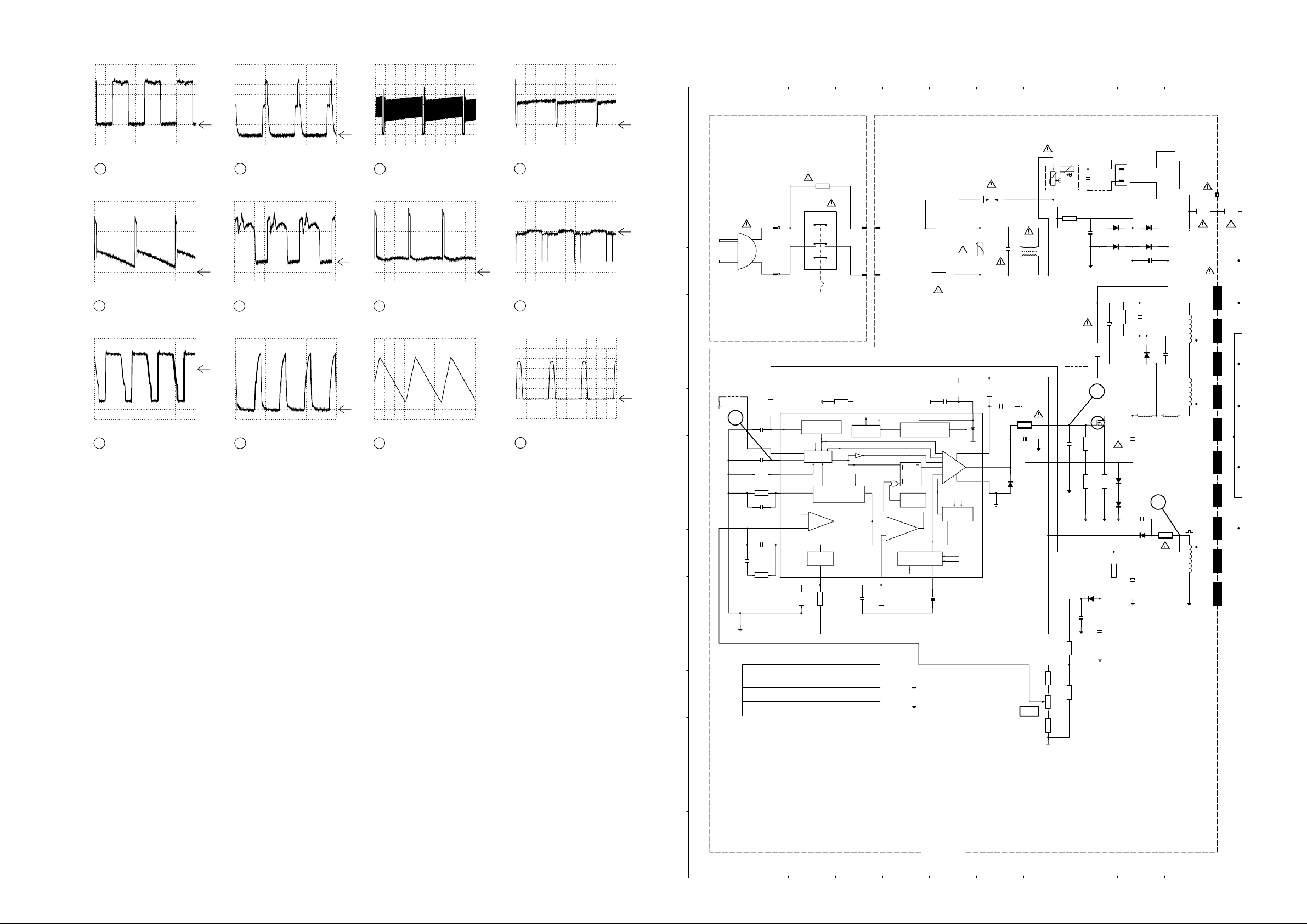
Platinenabbildungen und Schaltpläne / Layout of PCBs and Circuit Diagrams TVR 3710 …, TVR 5100 …, TVR 5500 … Platinenabbildungen und Schaltpläne / Layout of PCBs and Circuit Diagrams TVR 3710 …, TVR 5100 …, TVR 5500 …
Ubat
HOT PART
OUT VDR
Degaussing Coil
COLD GND
HOT GND
CIRCUIT, A VARIABLE ISOLATION TRANSFORMER IS REQUIRED.
THE INPUT VOLTAGE SLOWLY, WHEN TROUBLESHOOTING THIS TYPE OF POWER SUPPLY
TRANSFORMER MUST BE USED. ALSO, IN ORDER TO HAVE THE ABILITY TO INCREASE
BECAUSE A HOT GROUND IS PRESENT IN THE POWER SUPPLY CIRCUIT, AN ISOLATION
290V
329V
2,2V
2,3V
13V
13,5V
2,5V
0,3V
2,6V
2,6V
0,3V
2,5V
2,3V
1,3V
2,4V
50
451 678910111223
M
L
K
P
J
I
H
G
F
E
D
C
B
A
O
N
451 678910111223
75E
3347
3312
3M9
68E
3333
3337
2E
0E82
3334
20k
3357
9k1
3356
3304
270E
18k
3322
100k
3324
10k
3330
5k1
3327
1k
3339
0E82
3335
33k
3328
56k
3342
180k
3348
330E
3359
270k
3331
3313
3M9
20k
3362
5k6
3363
24k
3345
9318
9315
9314
9311
9310
9303
9309
5E6
3341
39E
3338
5354
80E
5350
80E
2325
560p
1n
2312
2323
4n7
100n
2337
4n7
2338
470p
2328
2n2
2305
2n2
2314
2341
2n2
470p
2327
2329
82p
2310
100n
1n
2324
2331
10n
470p
2332
4n7
2330
220p
2336
2n2
2301
2308
1n
2309
4n7
220n
2316
BYT54
6337
BYT54
6336
1N5062
6316
1N5062
6314
1N5062
6313
1N5062
6315
BAV21
6335
BYD33D
6334
BYT54
6332
BYV10-20
6348
100u
2335
68u
2315
2u2
2320
5330
1
3
4
5
6
7
2
8
STP4NA60FI
7330
DMF-2830
5311
1300
T2,5AH
1311
3310
1
2
3
1013
1013
1924
1
2
4k7
3358
SIQV-S10K300
3309
7310
MC44603P
10
11
12
13
14
15
16 1
2
3
4
5
6
7
8
9
(REDUCED FREQUENCY)
AMP
ERROR
FOLDBACK
MANAGEMENT
OSCILLATOR
Iref
DEMAGNETICATION
Vdem out
STANDBY
2.5V
P
F
T
FOLDBACK INPUT
E/A OUT
R standby
Sync
R standby
VOLTAGE
C
FEEDBACK
Vdem in
CURRENT SENSE INPUT
Vosc
REFERENCE
Vref
BLOCK
Iref
enable
Vref
CURRENT
SENSE
Vosc prot
Iref
Dmax & SOFT-START
INITIALIZATION BLOCK
Set
Latch
Reset
SHUTDOWN
THERMAL
CONTROL
SUPPLY &
Q
Rref
Soft Start & Dmax
Iref
Vovp out
Vref
BUFFER
OVERVOLTAGE
MANAGEMENT
UVLO1
Vref
OVERVOLTAGE
PROTECTION
UVLO1
Vcc
Vcc
OUTPUT
GND
18V
Vc
CAUTION : LETHAL POTENTIALS AT PRIMARY
DO NOT OPERATE WITHOUT CASE
ISOLATION TRANSFORMER WHEN SERVICING
HOT CIRCUIT , BE CAREFUL AND USE AN
1301
IN
1013
1013
1003
1
23
4
2
1
3302
4M7
51
52
SWITCH PCB
Leistungs-Chassis / Power Chassis TVR 5500 … (PLSP)
TV
TV
TV
TV
DC, 500mV/Div, 20µs/Div
IC7200-(37), Connector 1922-(4)
33
DC, 10V/Div, 5ms/Div
IC7510-(5)
46
DC, 10V/Div, 5µs/Div
Trafo 5330-(4), 5331-(4)
50
0V
TV
0V
PB
0V
DC, 1V/Div, 20µs/Div
IC7200-(38), Connector 1922-(5)
34
TV
DC, 200mV/Div, 20µs/Div
T7584 – Basis
47
PB
DC, 2V/Div, 5µs/Div
T7330 – Gate
51
0V
AC, 1V/Div, 5ms/Div
IC7200-(43), Connector 1922-(1)
43
0V
DC, 5V/Div, 5ms/Div
IC7510-(8)
48
0V
AC, 500mV/Div, 10µs/Div
IC7310-(10)
52
TV
STANDBY
DC, 1V/Div, 5ms/Div
IC7510-(1)
45
0V
DC, 5V/Div, 20µs/Div
T7583 – Basis
49
DC, 200V/Div, 20µs/Div
T7583, Collector
53
0V
TV
0V
TV
0V
4 - 29 GRUNDIG Service 4 - 30 GRUNDIG Service
Page 56
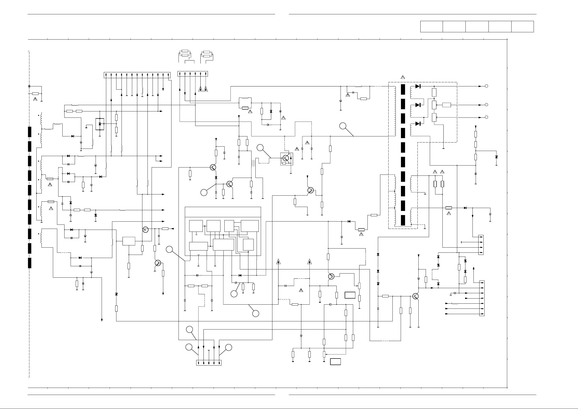
TVR 3710 …, TVR 5100 …, TVR 5500 … Platinenabbildungen und Schaltpläne / Layout of PCBs and Circuit Diagrams
Reference
AL ..............P 4-65
BUPI ..........P 4-68
CO .............P 4-43
DE..............P 4-49
IO...............P 4-59
OHA...........P 4-69
PLSP .........P4-19
PSSP2.......P 4-37
TU2............P 4-55
T
ube PCB
...P 4-33
TV..............P 4-51
TXT............P 4-58
VS..............P 4-61
TVR 3710 …, TVR 5100 …, TVR 5500 … Platinenabbildungen und Schaltpläne / Layout of PCBs and Circuit Diagrams
2312
1n
3313
3M9
32 33 3412 13 14 15 16 17 18 19 20 21 22 23 24 25 26 27 28 29 30 31
DEFLECTIONVERTICALHORIZONTAL
to Signal Chassis (TV) 1909
33A
5A
7350
LM317T
5
3351
GNDM
1
GNDM
6
MTP3055E
2k7
5D
789
22u
5352
7352
5,29V
3352
GND5D
5351
5,1V
80E
820E
5353
BC548B
22u
7351
GND5A
10
14,2V
3353
STBY
111213
STBY
33A
14H
14H
-7V
3354
220k
100n
2353
1k
43mV
3350
STBY
5Stby
HDEF1
1925
1
5D1
9A
14H
45
10k
Ubat
Ubatlot
HDEF2
VDEFH
VDEFL
2
3
4
5
6
VDEFH
VDEFL
8
8V
680E
100n
2594
3577
4,8V
1,4V
7587
BC548B
TDA3654/N3
Protection
3k9
9517
0,95V
BAV21
6583
0,47V
330p
2581
Output
Stage
Output Stage
45
1n
2517
3588
150E
Guard
Circuit
4k7
3580
47
Thermal
Protection
Driver
GND
2,2V
23
1
0V 2,2V 15,5V0V 28,6V 1,8V 6,3V 28,3V
2514
1n
3536
3530
3k9
2n2
2515
Ubat
82,7V
3596
2552
17,2V
7584
MPSA43
7510
6
6513
BYD33D
2513
100u
48
5510
3310
3527
1k
6k8
6k8
3598
100n
5581
2k2
3585
1n
2583
Voltage Stab.
&
Current Source
Flyback
Generator
78
1k5
3513
3512
46
3587
49
9523
CU15
9
1k
33k
2587
10u
6582
BYD33D
7583
BU1508DX
2584
VDEFH
9514
680n
9522
2516
100n
5551
3582
BYD33J
6592
6584
56k
6581
ANODE TO CRT
FOCUS
SCREEN
Ubat
3540
3541
3551
2551
8
BZX79-C4V7
BAV21
4k7
3584
TO TUBE PCB/1991
TO TUBE PCB/1993
10k
10k
30k
33n
1926
1
2
3
4
1923
1
2
3
4
5
6
7
2592
VRGB
GNDA
HEATER
AQUADAG
8
PROT
BCI
VCOMP
GND9A
9A
-7V
6555
4u7
2593
5590
47u
2589
10n
3589
47u
39E
9521
2
400M
focus
screen
53
9529
12n
1n5
2585
2586
86V
5D1
5,2V
7585
3599
3517
330E
0,96V
BC548B
1k
9512
1,1V
VDEFL
3579
3594
3595
BC558B
1k
7578
150k
15k
28,3V
3578
2520
100u
3597
220E
150k
3518
3538
BYD33D
6511
470u
2512
v-shift
1k
3519
3529
2k7
2E7
3531
2E7
9515
3524
4k7
10k
6553
6556
6554
2555
BAV21
BAV21
BZX79-C24
3554
47k
100n
1
8911
G
6
5
4
3553
10
5E6
4E7
3537
3532
6551
6552
6550
BAV21
BAV21
GNDAU
9A
-7V
3592
8E2
BZX79-C10
2582
220n
5556
80E
7
3
9520
5D1
9528
10u
2553
4k7
3555
4,9V
14mV
7550
BC548B
68k
22k
3558
14M2
14M1
14/9M1
1921
1
5361
33u
3391
3393
3k9
6361
BYW36
6371
BYW98-200
2371
470p
6372
BYW98-200
2381
470p
1n5
BAV21
2392
6351
BYW98-200
2351
470p
3k9
2362
5370
80E
3372
6392
3360
390E
10u
6374
BYT54
2378
1n
2375
3375
180E
9
5363
80E
5365
80E
12
15
13
1371
T2,5A
1372
T2,5A
9302
2377
9312
14
15
16
15
11
10
100u
2379
390E
1k
3364
1n
560u
7331
TL431CLP
5366
2374
2352
22u
2373
680u
6393
680u
32V
K
A
680u
6373
BYV10-20
BZX85-C6V8
GNDAU
R
5373
14M2
2
3
4
3394
100k
2,45V
8k2
3395
22u
22u
5372
5371
22u
5364
80E
23
22u
5374
8,5V
4,1V
6343
BZX79-C9V1
10k
3343
33
2519
43
3
VDR
4
2
VFB
HDR
GNDTV
1
1922
to Signal Chassis (TV) 1911
5
HFB/SC
34
3559
2200u
22E
3522
3525
1E5
3523
100E
v-amp
1E8
3521
10k
3556
270E
9524
32 33 3412 13 14 15 16 17 18 19 20 21 22 23 24 25 26 27 28 29 30 31
1003 C 3
1013 C 4
1013 D 4
1300 B 7
1311 D 5
1371 G13
1372 H13
A
1921 B15
1922 P20
1923 L33
1924 B 9
1925 B19
1926 I33
2301 B 9
2305 D10
2308 G 7
2309 H 8
B
2310 G 6
2312 B12
2314 C 9
2315 E 9
2316 D 7
2320 K 6
2323 J 2
2324 J 2
2325 I 2
C
2327 H 2
2328 H10
2329 G 2
2330 H 8
2331 E10
2332 F10
2335 K10
2336 I10
2337 K 9
D
2338 L 9
2341 K 4
2351 J14
2352 K15
2353 J18
2362 E14
2371 F14
2373 F15
2374 G15
E
2375 L14
2377 H13
2378 K14
2379 J14
2381 G14
2392 I14
2512 J27
2513 L22
BZX79-B30
2514 K20
F
2515 M19
2516 L24
2517 M20
2519 N25
2520 M26
2551 G33
2552 F22
2553 L30
2555 M28
G
2581 G21
2582 L32
2583 G22
2584 D24
2585 E25
2586 E25
2587 D23
2589 C27
H
2592 I34
2593 C27
2594 F21
3302 B 3
3304 B 6
3309 D 6
3310 B 8
3312 C11
3313 C12
I
3322 K 3
3324 J 2
3327 I 2
3328 H 2
3330 G 4
3331 F 9
3333 G 7
3334 H 9
3335 H 9
J
3337 C 8
3338 G 8
3339 H 9
3341 J11
3342 G 2
3343 M16
3345 E10
3347 J 9
3348 K 3
K
3350 K18
3351 K16
3352 J17
3353 J18
3354 I18
3356 L 8
3357 M 8
3358 M 8
3359 K 4
L
3360 H14
3362 N 8
3363 M 8
3364 H14
3372 G14
3375 L14
3391 C14
3393 C14
M
3394 D16
3395 D16
3512 L22
to Signal Chassis (TV) 1912 to TUBE PCB 1969
3513 L22
3517 M24
3518 L26
3519 M27
3521 N27
3522 O26
N
3523 O26
3524 L28
3525 O25
3527 C22
3529 M27
3530 L20
3531 I28
3532 G31
3536 L19
O
3537 G31
3538 H28
3540 E33
3541 E33
3551 F33
3553 M29
3554 L29
3555 L31
3556 N27
3558 M30
3559 O24
P
3577 F21
3578 K26
3579 L26
3580 G19
3582 K32
3584 L33
3585 G22
3587 D23
3588 G21
3589 C28
3592 H32
3594 F26
3595 H26
3596 E22
3597 E26
3598 E22
3599 H24
5311 C 8
5330 D11
5330 G10
5351 C17
5352 G17
5353 G17
5354 G11
5361 C14
5363 D13
5364 H16
5365 D13
5366 E15
5370 F14
5371 E16
5372 E16
5373 F15
5374 J16
5510 C22
5551 B31
5556 M32
5581 F22
5590 B27
6313 C 9
6314 C 9
6315 C10
6316 C10
6332 F10
6334 J10
6335 K 9
6336 H 9
6337 I 9
6343 L16
6348 I 7
6351 I14
6361 E14
6371 F14
6372 G14
6373 G15
6374 K14
6392 H14
6393 I15
6511 I27
6513 K22
6550 L31
6551 K31
6552 K31
6553 J28
6554 L28
6555 F34
6556 K28
6581 K32
6582 D23
6583 G21
6584 K32
6592 H33
7310 G 5
7330 G 9
7331 D15
7350 J16
7351 K18
7352 I17
7510 H22
7550 L30
7578 L26
7583 E23
7584 G21
7585 G25
7587 F21
9302 G13
9303 F 9
9309 G 6
9310 C 5
9311 D 5
9312 J13
9314 B 9
9315 B 9
9318 G 1
9512 L25
9514 M24
9515 K28
9517 M20
9520 I30
9521 B28
9522 E24
9523 F23
9524 O29
9528 K31
9529 D25
GRUNDIG Service 4 - 31
GRUNDIG Service 4 - 32
Page 57
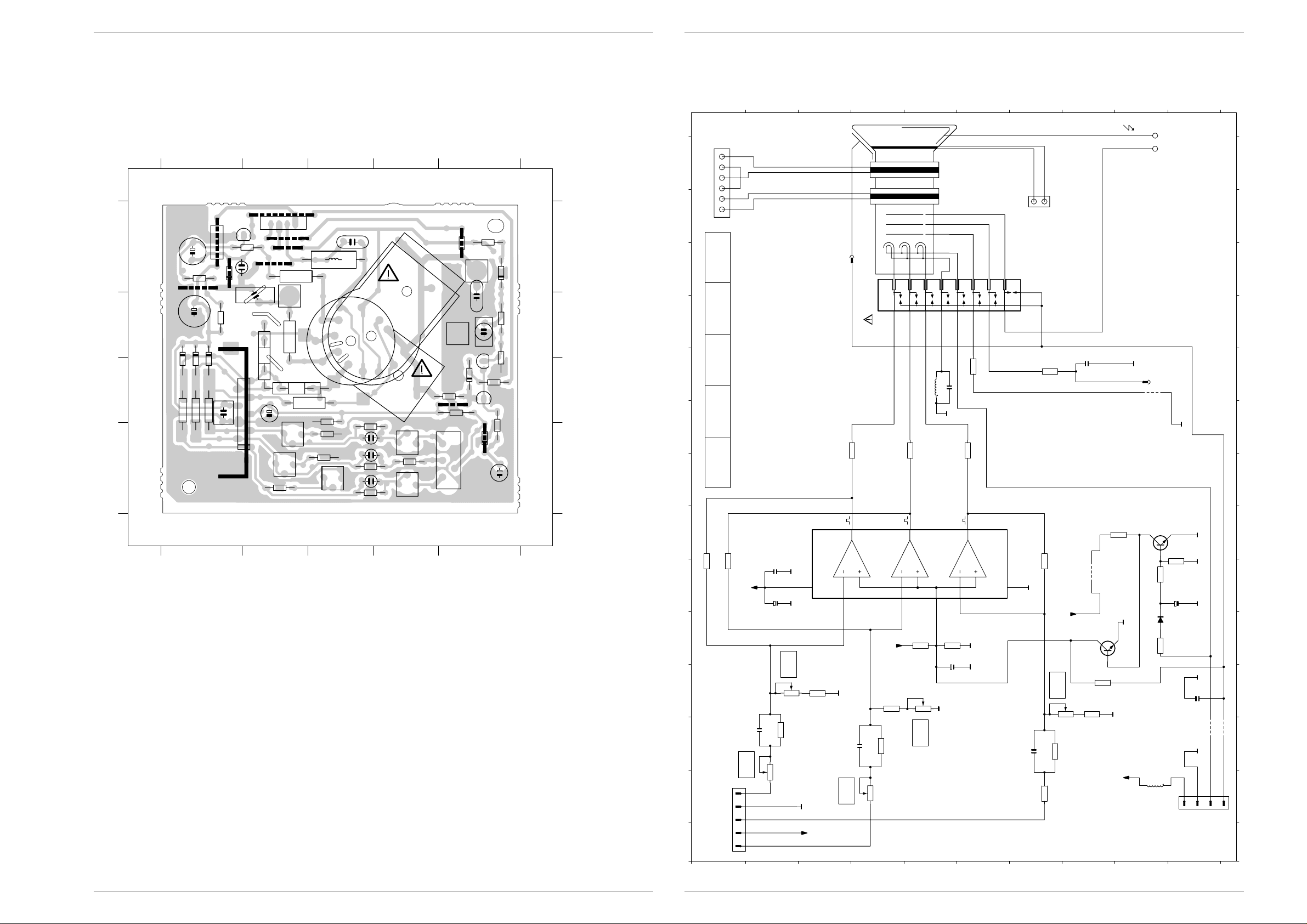
Platinenabbildungen und Schaltpläne / Layout of PCBs and Circuit Diagrams TVR 3710 …, TVR 5100 …, TVR 5500 … Platinenabbildungen und Schaltpläne / Layout of PCBs and Circuit Diagrams TVR 3710 …, TVR 5100 …, TVR 5500 …
TO POWER PCB 1925
SCREEN
B-Gain
G-Gain
1920
TO POWER PCB 1926
ANODE
L5550
1924
TO POWER PCB
FOCUS
TO FAMILYBOARD 1913
R
G
B
8
GNDTV
HEATER
GNDA
AQUADAG
VRGB
DEG1
DEG2
TO POWER PCB
Uref
B-Cutoff
G-Cutoff
R-Cutoff
(TV-part)
105V
105V
115V
178V
1,3V
1,3V
1,3V
1,3V
0V
7,4V
0,65V
40mV
9905 I10
9903 H 6
9902 J 3
9901 K 3
7902 I 7
7901 H 5
7900 C 6
6906 J 5
5902 I 2
5901 E10
3936 I 6
3932 I 5
3931 J 6
3930 I 7
3925 G10
3922 H 4
3921 B 2
3920 H 3
3919 D 2
3918 E 3
3917 B 4
3916 F10
3915 E 9
3914 F 9
3913 C 9
3912 A 6
3911 A 6
3910 G 6
3909 E 5
3908 E 5
3907 G 3
3906 H 3
3905 D 4
3904 D 3
3903 C 4
3902 B 3
3901 G 2
2913 J 6
2909 E10
2908 B 6
2907 H10
2906 B 6
2905 E 4
2904 G 3
2903 D 3
2902 B 3
2901 J 4
1969 J 2
1967 A 2
1962 D12
1961 D11
451 6 7 8 9 10 11 12 13 1423
H
G
F
E
D
C
B
A
J
I
451 6 7 8 9 10 11 12 13 1423
2k2
3936
4k7
3932
4k7
3931
18k
3930
1k5
3914
1k5
3913
680E
3901
820E
3906
5k6
3902
820E
3903
5k6
3904
820E
3905
5k6
3907
8k2
3908
1k5
3909
82k
3910
82k
3911
82k
3912
1k5
3915
1k5
3916
1k5
3925
560k
3922
8
8
+180V
+180V
8
7901
BC548B
7902
BC548B
9905
9903
9902
9901
330u
5902
10u
5901
4u7
2913
10u
2908
10u
2905
1n
2909
1n
2901
7p
2902
7p
2903
7p
2904
100n
2906
10n
2907
6906
BAV21
2k2
3921
2k2
3919
470E
3920
470E
3917
470E
3918
1961
4454-S
6
8
4
5
210
1
TDA6103Q/N2
7900
1
2
3
4
5
6
7
8
9
1962
1969
1
2
3
4
1967
1
2
3
4
5
Reference
AL ..............P 4-65
BUPI ..........P 4-68
CO .............P 4-43
DE..............P 4-49
IO...............P 4-59
OHA...........P 4-69
PLSP .........P 4-19
PSSP2.......P 4-37
TU2............P 4-55
T
ube PCB
...P 4-33
TV..............P 4-51
TXT............P 4-58
VS..............P 4-61
Bildrohrplatte / Tube PCB
1967 —> Signal-Chassis (1913)
1969 —> Leistungs-Chassis / Power Chassis (1926)
1962 —> Bildröhre / CRT
Ansicht von der Bestückungsseite / View of Component Side
A
B
C
D
4 - 33 GRUNDIG Service 4 - 34 GRUNDIG Service
6903
2908
3912
12345
3932
1962
6906
2901
3936
2913
3931
7902
3933
7901
3930
9903
6905
2912
3922
1964
3908
9901
3924
2914
6907
1967
9924
3929
2910
3926
3914
9904
1969
3927
3905
9923
9902
3920
2905
3916
3917
2909
5901
5
96
1
6
6
9
1
3925
3915
9
1
6
2904
2903
1
3921
3919
9921
3901
3913
3909
3903
3906
3918
3902
2902
3907
3904
7903
5902
9906
2911
3934
9922
6902
6904
2907
9905
3935
6901
3911
3910
2906
7900
0030
12345
0030 C 2
1961 B 4
1962 A 5
1964 B 5
1965 C 3
1966 C 3
1967 D 5
1969 A 2
2901 B 5
2902 D 3
A
2903 D 3
2904 D 3
2905 C 2
2906 C 1
2907 B 2
2908 B 1
2909 A 3
2910 A 1
2911 A 1
2912 D 5
B
2913 B 5
2914 B 5
3901 D 4
3902 D 3
3903 D 3
3904 D 3
3905 D 2
3906 D 3
3907 D 3
C
3908 C 5
3909 C 3
3910 C 1
3911 C 1
3912 C 1
3913 C 3
3914 C 2
3915 C 2
3916 A 2
3917 D 2
D
3918 D 3
3919 D 4
3920 D 2
3921 D 4
3922 C 5
3924 A 5
3925 B 2
3926 B 2
3927 C 2
3929 A 2
3930 D 5
3931 C 5
3932 A 5
3933 C 5
3934 A 1
3935 B 1
3936 B 5
5901 A 3
5902 A 1
6901 C 1
6902 C 1
6903 C 1
6904 A 1
6905 D 5
6906 A 5
6907 C 5
7900 C 2
7901 C 5
7902 C 5
7903 A 2
9901 A 5
9902 A 2
9903 D 5
9904 A 2
9905 A 1
9906 A 1
9921 C 5
9922 A 1
9923 A 2
9924 A 2
Bildrohrplatte / Tube PCB TVR 3710 …
Page 58
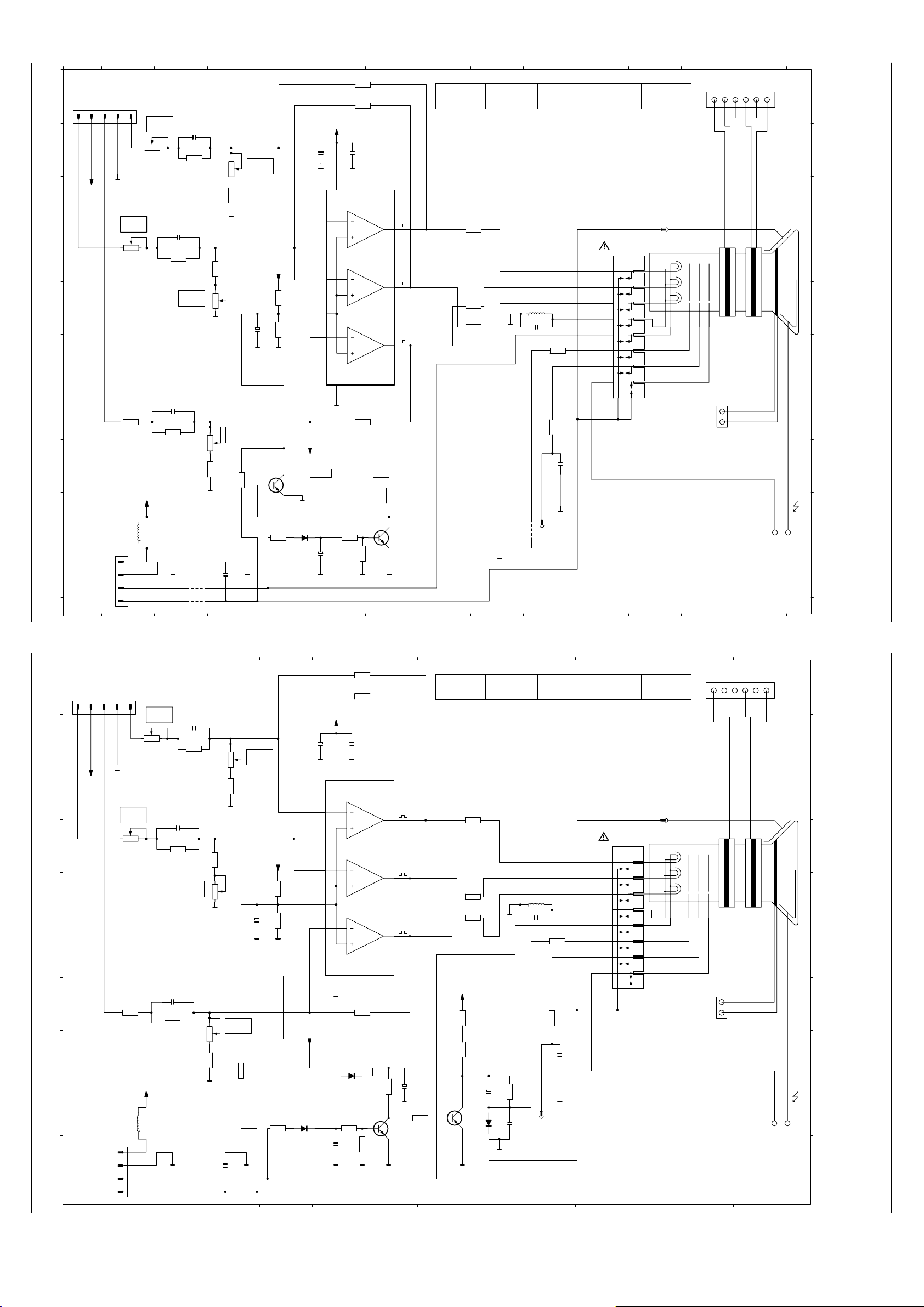
0
TO POWER PCB 1925
SCREEN
B-Gain
G-Gain
1920
TO POWER PCB 1926
ANODE
L5550
1924
TO POWER PCB
FOCUS
TO FAMILYBOARD 1913
RGB8GNDTV
HEATER
GNDA
AQUADAG
VRGB
DEG1
DEG2
TO POWER PCB
Uref
B-Cutoff
G-Cutoff
R-Cutoff
(TV-part)
105V
105V
115V
178V
1,3V
1,3V
1,3V
1,3V
0V
7,4V
0,65V
40mV
40mV
164V
9902 J 3
9901 K 3
7903 I 8
7902 I 7
7900 C 6
6906 J 5
6905 I 6
6904 I 9
5902 I 2
5901 E10
3936 I 6
3935 G 8
3934 H 8
3933 I 8
3932 I 5
3931 J 6
3930 I 7
3929 I 9
3927 E 9
3926 E 9
3925 G10
3922 H 4
3921 B 2
3920 H 3
3919 D 2
3918 E 3
3917 B 4
3916 F10
3913 C 9
3912 A 6
3911 A 6
3910 G 6
3909 E 5
3908 E 5
3907 G 3
3906 H 3
3905 D 4
3904 D 3
3903 C 4
3902 B 3
3901 G 2
2914 J 6
2912 I 7
2911 I 9
2910 I 9
2909 E10
2908 B 6
2907 H10
2906 B 6
2905 E 4
2904 G 3
2903 D 3
2902 B 3
2901 J 4
1969 J 2
1967 A 2
1966 D11
1962 D12
451 6 7 8 9 10 11 12 13 1423
H
G
F
E
D
C
B
A
J
I
H
G
F
E
D
C
B
A
J
I
451 6 7 8 9 10 11 12 13 1423
2k2
3936
100k
3935
100k
3934
39k
3933
4k7
3932
4k7
3931
6k8
3930
3M3
3929
1k5
3927
1k5
3926
1k5
3913
470E
3901
680E
3906
3k3
3902
680E
3903
3k3
3904
680E
3905
3k3
3907
8k2
3908
1k5
3909
82k
3910
82k
3911
82k
3912
1k5
3916
1k5
3925
390k
3922
1966
ISHM27S
5
7
9
10
12 14
1
+180V
8
8
+180V
+180V
8
7903
BF422
7902
BC548B
9902
9901
330u
5902
22u
5901
22u
2912
4u7
2911
10u
2908
10u
2905
1n
2910
1n
2909
1n
2901
10p
2902
10p
2903
10p
2904
100n
2906
10n
2907
100n
2914
6906
BAV21
6905
BAV21
6904
BAV21
2k2
3921
2k2
3919
220E
3920
220E
3917
220E
3918
TDA6103Q/N2
7900
1
2
3
4
5
6
7
8
9
1962
1969
1
2
3
4
1967
1
2
3
4
5
GRUNDIG Service 4 - 35
Reference
AL ..............P 4-65
BUPI ..........P 4-68
CO .............P 4-43
DE..............P 4-49
IO...............P 4-59
OHA...........P 4-69
PLSP .........P4-19
PSSP2.......P 4-37
TU2............P 4-55
T
ube PCB
...P 4-33
TV..............P 4-51
TXT............P 4-58
VS..............P 4-61
Reference
AL ..............P 4-65
BUPI ..........P 4-68
CO .............P 4-43
DE..............P 4-49
IO...............P 4-59
OHA...........P 4-69
PLSP .........P4-19
PSSP2.......P 4-37
TU2............P 4-55
T
ube PCB
...P 4-33
TV..............P 4-51
TXT............P 4-58
VS..............P 4-61
TO FAMILYBOARD 1913
A
RGB8GNDTV
2
3
4
5
B
8
C
G-Gain
2k2
D
3919
E
F
G
3901
820E
1
2k2
1967
B-Gain
3921
(TV-part)
2903
10p
3904
3k9
2904
10p
3907
3k9
2902
10p
3902
3k9
G-Cutoff
3920
3905
3918
470E
3917
3903
820E
470E
R-Cutoff
451 6 7 8 9 10 11 12 13 1423
470E
820E
B-Cutoff
2905
TVR 3710 …, TVR 5100 …, TVR 5500 … Platinenabbildungen und Schaltpläne / Layout of PCBs and Circuit Diagrams
Bildrohrplatte / Tube PCB TVR 5100 … Bildrohrplatte / Tube PCB TVR 5500 …
1962 D12
3911
82k
3912
82k
+180V
10u
100n
2906
2908
178V
7900
6
TDA6103Q/N2
1,3V
1
8
1,3V
2
8k2
3908
10u
3909
1,3V
Uref
5
1,3V
1k5
3
4
115V
9
105V
8
105V
7
0V
3910
82k
8
3913
1k5
3927
1k5
3926
1k5
5901
10u
2909
1962
1966
ISHM27S
1n
3916
1k5
9
10
5
7
1
12 14
TO POWER PCB
1k5
3925
TO POWER PCB 1925
DEG1
1920
DEG2
1924
1966 D11
1967 A 2
1969 J 2
A
2901 J 4
2902 B 3
2903 D 3
2904 G 3
2905 E 4
2906 B 6
2907 H10
2908 B 6
2909 E10
2913 J 6
3901 G 2
B
3902 B 3
3903 C 4
3904 D 3
3905 D 4
3906 H 3
3907 G 3
3908 E 5
3909 E 5
3910 G 6
3911 A 6
C
3912 A 6
3913 C 9
3916 F10
3917 B 4
3918 E 3
3919 D 2
3920 H 3
3921 B 2
3922 H 4
3925 G1
D
3926 E 9
3927 E 9
3930 I 7
3931 J 6
3932 I 5
3936 I 6
5901 E10
5902 I 2
6906 J 5
7900 C 6
E
7901 H 5
7902 I 7
9901 K 3
9902 J 3
9903 H 6
9905 I10
9906 I 2
F
G
H
I
J
GRUNDIG Service 4 - 36
1969
VRGB
4
GNDA
HEATER
AQUADAG
TO POWER PCB 1926
3
2
1
+180V
5902
330u
9906
9902
9901
3906
820E
3922
1n
2901
451 6 7 8 9 10 11 12 13 1423
560k
3932
4k7
7901
BC548B
BAV21
6906
2913
4u7
10n
3936
9903
2k2
3931
0,65V
4k7
7,4V
40mV
3930
7902
BC548B
18k
9905
SCREEN
2907
ANODE
FOCUS
TO POWER PCB
L5550
H
I
J
TVR 3710 …, TVR 5100 …, TVR 5500 … Platinenabbildungen und Schaltpläne / Layout of PCBs and Circuit Diagrams
Page 59
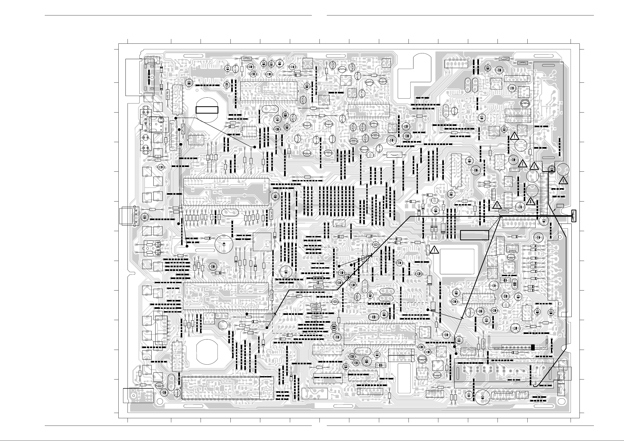
Platinenabbildungen und Schaltpläne / Layout of PCBs and Circuit Diagrams TVR 3710 …, TVR 5100 …, TVR 5500 … Platinenabbildungen und Schaltpläne / Layout of PCBs and Circuit Diagrams TVR 3710 …, TVR 5100 …, TVR 5500 …
8203 170 6375.3
3103 103 39580
PSSP2
1
B
C
B
E
C
E
B
CE
B
C
E
1 2345678910111213 14
1 2345678910111213 14
L
K
J
I
H
G
F
E
D
C
B
A
L
K
J
I
H
G
F
E
D
C
B
A
()
1
1
(40)
48
8
71
14
32
33
1
32
33
14
1
1
4
58
1
VCD- WI RES
7
8
VCD- DRAEHT E
20
( 21)
)(
6
10
1
5
22
21
24
1
25
8
9
16
64
1
1
64
42
1
8
9
1
8
1
16
27
9
26
)(
(
1
)(
1
32
1
52
16
))(
(
1
)
16
17
1
12
13
VCD- DRAEHTE
VCD- WI RES
1
18 10
9
1
1
1
1
()
1
24
1458
1
1
1
1
1
1
1
8
4
5
()
1
1
1
21
)(
1916
3244
3249
9196
1854
1856
1858
1853
1857
0005
0008
1850
1861
3878
3879
7811
1851
1859
2815
3835
0010
0007
0009
3868
3869
68636868
6869
7812
1918
1919
1860
9033
5881
7880
7881
2881
1876
5880
3236
1907
1800
1874
7870
9166
9170
9233
9162
9163
9164
9165
9167
9168
9201
9161
7801
1877
1908
3235
3237
1802
1873
9134
9135
9136
9137
9138
9139
9208
CD42
CD84
3898
6802
6860
6861
9109
9110
3823
3825
3829
1870
1881
3403
3410
3412
3414
3416
3441
9160
7410
9107
3420
3418
1871
1879
2513
9140
7840
CD53
CD54
CD55
5840
7813
6862
3853
1872
1878
1880
1972
9098
6517
9005
5841
6516
2065
9169
9151
9171
9172
9173
9177
9197
9215
9236
CD83
6804
6805
3838
3824
3811
3816
3214
2814
1801
1803
9108
9133
9206
9218
3830
3831
6803
6830
3473
1804
2802
2808
3408
3433
3438
3440
3470
3423
9090
9093
3461
3478
3434
3447
3425
1400
9017
9034
9035
9214
CD41
9008
9010
9011
6070
7070
3071
9006
9007
7051
5001
3005
5015
2018
2061
2017
2015
2016
9131
9182
9183
9185 1913
9194
9178
9179
9180
9181
9184
9186
9188
9189
6208
6261
6262
7201
7202
3218
1502
9211
9212
CD85
9121
9130
9143
9153
9157
9158
9174
9195
9227
5202
5801
6200
6263
5203
5200
5201
3743
3822
9145
9149
9150
9198
9219
9220
9221
9222
9223
9225
9226
9042
9043
9044
9073
9111
9112
9114
9118
9123
9142
5401
5882
6801
2801
3436
9099
9101
9102
9103
9104
9105
9106
9205
9025
9038
9091
9096
9100
2401
3427
3435
9012
9018
9021
9031
5012
5013
5008
5007
3115
5006
3031
1000
2004
2005
2007
2009
9015
9016
5003
6000
3030
3011
3010
2029
2020
2022
2023
2027
1750
9187
7754
9152
7200
2219
2230
2742
2743
2744
2223
1200
9141
9075
9113
9176
9224
5706
2733
2748
2805
2810
2811
3220
1740
2224
2231
2510
CD51
CD52
9078
9119
9144
9147
9203
9204
9213
6515
6513
3526
1973
2715
3515
2508
9082
9083
9084
9085
9086
9087
9095
9019
9024
9026
9030
9039
9040
9049
9050
9053
9081
9028
9029
7151
9027
5112
5113
7006
5114
5005
5106
5107
5110
5111
5004
5014
5002
3020
9020
5010
5100
5101
5102
5011
5105
5009
3029
3027
3028
1911
3207
9023
9159
5704
5707
5701
5702
5705
3202
2712
2713
1720
1732
2200
2203
9146
1745
1746
9200
9229
CD21
9014
9132
9199
9202
6203
2229
9148
9056
9067
9077
9079
9080
9088
9122
9116
6514
6692
6693
6512
2514
2511
2690
3270
3517
9009
9064
9065
9068
9076
9092
9216
9230
9232
6280
6690
6691
7690
9046
9047
9048
9051
9089
5115
9022
5000
5108
3114
2136
2058
2059
9041
9045
9207
5103
5104
2242
2701
3703
3704
9129
9191
CD22
CD23
5700
5703
7280
9193
3712
3729
3772
3250
2740
1
17 16 15 14 13 12 11 10 9 8
65
171615141312111098
65
701 1702
2244
7601
9072
9117
9156
6202
3740
5601
2609
2611
2615
2605
2616
9061
9062
9066
3606
3618
6205
6694
9054
9058
9069
9070
9097
9037
9060
7411
3494
3495
3690
3462
3463
2450
2452
2316
9001
9004
9057
9063
9231
9302
5307
3329
2455
1340
1345
9000
9301
2320
1902
1346
1912
1971
9235
9155
0006
9209
9124
9125
9127
9128
9192
6242
7240
9074
9175
9190
7604
7608
6500
6503
2614
3661
3539
2659
2622
2654
1915
2617
2619
2620
9071
6508
6509
5603
6401
6504
6505
6506
6507
6510
5602
2470
1900
1901
2251
1905
2491
1004
9052
9055
9059
9234
7402
7491
5402
3306
3452
1001
1002
1301
1903
1904
1909
1324
9003
9217
9303
3448
3322
3341
2430
2300
1320
1322
5304
5303
5305
5300
5301
5302
2324
2322
1970
3206
1914
9126
2501
9120
2301
2311
9115
9210
1003
1501
9002
Signal-Chassis (PSSP2)
Ansicht von der Bestückungsseite / View of Component Side
1909, 1911, 1912, —> Leistungs-Chassis / Power Chassis (1921, 1922, 1923)
1900, 1901, 1903, 1905 —> Laufwerk / Drive Mechanism (L8, L3, L4, L2)
1913 —> Bildrohrplatte / Tube PCB (1967)
1902, 1904 —> Kopfverstärkerplatte / Head Amplifier Board (1910, 1930)
1918, 1971 —> Buchsenplatte / Socket Board (1937, 1935)
1914, 1970 —> Lautsprecher
4 - 37 GRUNDIG Service
4 - 38 GRUNDIG Service
Page 60

TVR 3710 …, TVR 5100 …, TVR 5500 … Platinenabbildungen und Schaltpläne / Layout of PCBs and Circuit Diagrams
0005 F 1
0006 J 13
0007 D 1
0008 G 1
0009 C 1
0010 D 1
1000 B 5
1001 E 14
1002 E 14
1003 D 14
1004 D 13
1200 K 8
1301 B 14
1320 C 13
1322 A 13
1324 C 13
1340 B 11
1345 B 12
1346 B 11
1400 F 3
1501 E 14
1502 H 5
1701 K 13
1702 K 13
1720 K 9
1732 K 9
1740 H 8
1745 I 9
1746 I 9
1750 L 8
1800 L 2
1801 I 3
1802 I 3
1803 J 3
1804 G 5
1850 G 1
1851 E 1
1853 I 1
1854 K 1
1856 K 1
1857 J 1
1858 J 1
1859 E 1
1860 B 1
1861 H 1
1870 G 1
1871 E 1
1872 D 1
1873 I 1
1874 K 1
1876 J 1
1877 I 1
1878 C 1
1879 E 1
1880 B 1
1881 H 1
1900 G 13
1901 G 13
1902 A 11
1903 E 13
1904 E 13
1905 F 13
1907 J 1
1908 J 1
1909 E 14
1911 L 10
1912 L 13
1913 L 6
1914 K 14
1915 H 14
1916 L 1
1918 A 1
1919 A 1
1970 L 14
1971 L 13
1972 C 2
1973 F 7
2004 C 5
2005 C 5
2007 C 5
2009 C 5
2015 A 4
2016 B 3
2017 A 4
2018 A 5
2020 A 5
2022 A 5
2023 A 5
2027 A 6
2029 B 6
2058 C 9
2059 C 9
2061 A 3
2065 B 2
2136 C 9
2200 K 9
2203 K 8
2219 J 7
2223 I 8
2224 H 8
2229 I 9
2230 K 8
2231 I 8
2242 L 12
2244 J 11
2251 G 14
2300 C 13
2301 D 14
2311 D 14
2316 C 12
2320 A 12
2322 B 13
2324 A 13
2401 E 5
2430 D 13
2450 E 11
2452 D 12
2455 D 12
2470 F 14
2491 F 13
2501 I 14
2508 H 7
2510 G 8
2511 H 9
2513 D 1
2514 H 10
2605 H 12
2609 I 11
2611 I 11
2614 I 12
2615 I 12
2616 J 12
2617 I 13
2619 I 13
2620 H 13
2622 H 13
2654 J 13
2659 I 14
2690 F 10
2701 L 12
2712 J 10
2713 K 10
2715 H 7
2733 I 8
2740 J 11
2742 K 8
2743 K 8
2744 K 7
2748 I 7
2801 H 5
2802 G 3
2805 H 7
2808 H 3
2810 J 7
2811 J 7
2814 J 3
2815 F 1
2881 L 1
3005 A 4
3010 A 6
3011 A 6
3020 A 7
3027 A 7
3028 A 8
3029 B 7
3030 B 6
3031 D 5
3071 C 4
3114 C 10
3115 C 7
3202 L 11
3206 K 14
3207 L 9
3214 J 4
3218 K 6
3220 J 7
3235 J 2
3236 J 2
3237 J 2
3244 L 1
3249 K 1
3250 J 12
3270 G 10
3306 D 14
3322 C 12
3329 C 11
3341 C 13
3403 F 3
3408 F 3
3410 F 2
3412 F 2
3414 F 2
3416 F 2
3418 F 2
3420 F 2
3423 D 3
3425 D 3
3427 D 5
3433 F 3
3434 D 3
3435 E 6
3436 F 5
3438 F 4
3440 F 4
3441 F 3
3447 D 3
3448 D 12
3452 D 13
3461 D 4
3462 F 12
3463 E 11
3470 F 4
3473 F 4
3478 D 4
3494 E 12
3495 E 12
3515 G 8
3517 G 10
3526 G 8
3539 J 14
3606 H 12
3618 H 12
3661 J 14
3690 F 11
3703 L 11
3704 L 11
3712 K 10
3729 K 11
3740 J 10
3743 I 6
3772 K 11
3811 J 4
3816 H 4
3822 H 5
3823 H 2
3824 J 4
3825 H 2
3829 H 3
3830 H 4
3831 H 4
3835 F 1
3838 I 4
3853 C 1
3868 D 1
3869 D 1
3878 G 1
3879 G 1
3898 G 2
5000 D 9
5001 A 4
5002 D 8
5003 B 6
5004 C 7
5005 D 7
5006 C 6
5007 D 6
5008 C 6
5009 A 7
5010 A 7
5011 A 8
5012 C 6
5013 C 6
5014 C 7
5015 A 4
5100 B 8
5101 B 8
5102 A 8
5103 A 9
5104 A 9
5105 A 8
5106 C 7
5107 C 8
5108 C 9
5110 C 8
5111 C 8
5112 C 8
5113 C 8
5114 C 8
5115 D 9
5200 H 6
5201 I 6
5202 I 6
5203 I 6
5300 A 13
5301 B 13
5302 B 13
5303 B 12
5304 A 13
5305 B 13
5307 B 11
5401 F 5
5402 F 13
5601 I 12
5602 G 13
5603 H 13
5700 J 12
5701 K 10
5702 K 10
5703 K 10
5704 K 10
5705 J 10
5706 I 8
5707 K 10
5801 I 5
5840 C 2
5841 B 1
5880 L 1
5881 L 2
5882 H 6
6000 A 6
6070 C 4
6200 H 7
6202 I 10
6203 H 10
6205 F 11
6208 J 5
6242 K 13
6261 J 5
6262 K 6
6263 J 5
6280 F 10
6401 G 13
6500 H 14
6503 I 14
6504 H 14
6505 G 14
6506 H 14
6507 G 14
6508 H 14
6509 G 14
6510 H 14
6512 G 9
6513 G 8
6514 G 9
6515 G 7
6516 B 1
6517 A 1
6690 E 10
6691 F 10
6692 F 10
6693 F 10
6694 F 10
6801 G 5
6802 G 3
6803 H 3
6804 J 4
6805 H 4
6830 G 4
6860 G 1
6861 G 1
6862 C 1
6863 C 1
6868 C 1
6869 D 1
7006 D 8
7051 B 5
7070 C 4
7151 B 8
7200 J 9
7201 K 7
7202 K 7
7240 J 13
7280 K 12
7402 D 13
7410 E 3
7411 D 11
7491 E 12
7601 I 12
7604 I 13
7608 I 13
7690 E 10
7754 K 8
7801 I 3
7811 F 1
7812 C 1
7813 C 2
7840 B 2
7870 K 2
7880 L 3
7881 L 3
9000 A 12
9001 C 11
9002 D 14
9003 D 13
9004 C 12
9005 B 3
9006 B 4
9007 B 4
9008 C 4
9009 E 9
9010 C 4
9011 C 4
9012 C 5
9014 I 9
9015 A 6
9016 B 6
9017 C 4
9018 D 5
9019 E 8
9020 B 7
9021 C 5
9022 C 9
9023 K 9
9024 E 8
9025 D 5
9026 D 7
9027 D 7
9028 D 8
9029 D 8
9030 D 7
9031 C 5
9033 A 1
9034 D 3
9035 D 3
9037 D 11
9038 E 6
9039 D 7
9040 E 7
9041 B 10
9042 G 5
9043 G 6
9044 H 5
9045 B 10
9046 C 10
9047 C 10
9048 D 9
9049 D 8
9050 E 8
9051 D 10
9052 E 13
9053 E 7
9054 F 12
9055 F 14
9056 H 10
9057 C 11
9058 F 12
9059 F 12
9060 D 12
9061 F 11
9062 F 11
9063 D 12
9064 F 9
9065 E 9
9066 F 11
9067 F 10
9068 D 10
9069 D 10
9070 D 10
9071 H 13
9072 J 12
9073 G 6
9074 J 12
9075 H 8
9076 F 9
9077 F 9
9078 F 8
9079 F 9
9080 F 8
9081 F 7
9082 F 7
9083 F 7
9084 E 7
9085 E 7
9086 E 8
9087 E 8
9088 H 10
9089 D 10
9090 D 4
9091 D 5
9092 E 9
9093 D 4
9095 E 7
9096 E 6
9097 F 11
9098 D 2
9099 E 6
9100 E 6
9101 E 6
9102 E 5
9103 E 5
9104 F 5
9105 F 5
9106 F 5
9107 E 2
9108 F 3
9109 G 2
9110 G 2
9111 F 5
9112 G 5
9113 H 8
9114 G 6
9115 E 14
9116 G 9
9117 I 11
9118 H 6
9119 F 7
9120 F 14
9121 H 5
9122 G 9
9123 H 7
9124 K 14
9125 K 14
9126 J 14
9127 K 13
9128 L 13
9129 L 12
9130 J 6
9131 L 5
9132 I 10
9133 G 4
9134 G 2
9135 H 2
9136 H 2
9137 H 2
9138 H 2
9139 H 2
9140 D 2
9141 H 8
9142 F 6
9143 J 6
9144 F 7
9145 G 6
9146 H 9
9147 G 8
9148 H 9
9149 G 6
9150 G 6
9151 K 4
9152 L 8
9153 J 6
9155 L 14
9156 I 11
9157 J 6
9158 H 5
9159 J 11
9160 F 1
9161 I 1
9162 H 2
9163 I 2
9164 I 1
9165 I 2
9166 J 2
9167 J 2
9168 J 2
9169 J 4
9170 K 1
9171 J 3
9172 K 4
9173 K 4
9174 I 6
9175 I 14
9176 I 9
9177 J 4
9178 K 5
9179 K 5
9180 K 5
9181 J 5
9182 L 6
9183 L 6
9184 K 6
9185 L 5
9186 L 5
9187 K 8
9188 K 7
9189 K 7
9190 J 14
9191 K 11
9192 K 12
9193 K 12
9194 J 6
9195 J 6
9196 J 1
9197 K 4
9198 F 5
9199 I 9
9200 I 9
9201 H 1
9202 H 9
9203 F 8
9204 F 8
9205 D 5
9206 G 4
9207 B 10
9208 G 2
9209 L 14
9210 E 14
9211 I 7
9212 I 7
9213 H 7
9214 C 4
9215 K 5
9216 E 10
9217 D 14
9218 F 4
9219 G 6
9220 G 6
9221 G 5
9222 G 5
9223 G 5
9224 I 7
9225 H 6
9226 H 6
9227 I 6
9229 I 10
9230 E 9
9231 B 12
9232 D 10
9233 K 2
9234 E 13
9235 L 14
9236 K 4
9301 A 12
9302 C 11
9303 C 14
GRUNDIG Service 4 - 39
Page 61

Platinenabbildungen und Schaltpläne / Layout of PCBs and Circuit Diagrams TVR 3710 …, TVR 5100 …, TVR 5500 …
2000 B 6
2001 B 5
2002 B 5
2003 B 5
2006 B 5
2008 B 5
2010 B 4
2011 B 4
2012 B 4
2013 A 4
2014 A 4
2019 B 4
2021 B 5
2024 A 5
2025 B 5
2026 B 5
2028 B 6
2030 A 6
2031 B 5
2032 B 5
2033 B 6
2034 B 6
2035 A 7
2036 A 7
2037 A 7
2038 A 7
2039 B 6
2040 C 6
2041 B 7
2042 B 7
2043 C 6
2044 C 6
2045 C 6
2046 C 6
2047 C 6
2048 C 6
2049 D 6
2050 D 7
2051 D 7
2052 D 6
2053 C 7
2054 C 7
2055 C 7
2056 C 6
2060 A 3
2062 B 5
2064 A 3
2066 A 2
2067 B 3
2068 A 2
2069 B 3
2070 A 11
2071 C 4
2073 C 4
2075 C 4
2076 C 5
2100 A 9
2101 B 8
2102 B 8
2103 A 9
2104 B 8
2105 B 9
2106 A 8
2107 B 8
2108 A 9
2109 B 8
2110 B 9
2111 B 9
2112 B 8
2113 B 9
2114 A 8
2115 C 9
2116 A 9
2117 C 6
2118 C 7
2119 B 7
2121 C 7
2122 C 9
2123 B 8
2124 B 8
2125 C 7
2126 C 8
2127 C 8
2128 C 8
2129 C 9
2130 C 9
2132 C 8
2133 C 8
2134 C 8
2135 C 8
2201 J 9
2202 J 9
2204 J 9
2205 J 8
2206 K 8
2207 J 8
2208 J 8
2209 K 8
2210 K 6
2211 K 7
2212 K 7
2213 K 7
2214 L 7
2215 K 7
2216 J 6
2217 J 6
2218 K 7
2220 J 5
2221 J 5
2222 K 6
2225 H 7
2226 J 8
2227 J 9
2228 J 9
2240 K 12
2241 J 14
2243 K 14
2245 L 1
2246 L 1
2247 K 14
2248 I 9
2249 K 12
2250 G 14
2252 E 14
2253 E 14
2254 E 14
2255 F 14
2256 K 13
2258 K 14
2261 H 14
2262 K 6
2263 H 14
2280 J 11
2281 K 12
2302 B 14
2303 C 14
2304 B 14
2306 C 12
2307 C 13
2308 B 12
2309 A 12
2313 A 12
2314 B 12
2315 B 12
2317 C 12
2318 C 12
2319 C 12
2321 A 13
2323 C 11
2325 C 13
2327 B 11
2328 B 14
2329 B 13
2330 B 14
2331 B 14
2332 B 14
2333 C 14
2400 E 3
2403 E 5
2404 E 3
2405 E 3
2415 F 9
2427 D 2
2428 D 3
2429 F 13
2431 E 13
2432 D 13
2433 E 3
2451 E 11
2453 D 11
2454 E 11
2456 D 11
2457 F 13
2458 E 12
2471 E 2
2472 F 12
2473 F 12
2490 F 11
2502 H 14
2503 I 14
2504 I 14
2505 H 14
2506 H 14
2507 H 7
2509 A 1
2512 A 1
2515 A 1
2600 I 12
2601 H 12
2602 H 12
2604 H 12
2606 H 11
2607 I 11
2608 H 11
2612 I 11
2613 I 12
2618 H 13
2621 H 13
2626 J 13
2630 I 12
2651 J 13
2652 J 13
2653 I 13
2655 I 13
2656 I 13
2657 I 14
2658 I 13
2660 I 13
2661 J 13
2662 J 14
2691 E 10
2700 K 14
2702 K 12
2703 K 13
2708 K 10
2709 K 10
2710 K 10
2711 J 10
2714 J 9
2716 J 9
2717 I 10
2718 J 10
2719 J 11
2720 J 10
2721 J 10
2722 J 10
2723 I 10
2725 J 9
2726 I 9
2727 H 8
2728 H 9
2729 I 8
2730 J 9
2731 J 9
2732 I 8
2741 K 8
2745 K 8
2746 L 8
2747 K 8
2750 L 10
2803 I 3
2804 H 3
2806 I 4
2807 H 3
2809 J 8
2812 I 3
2813 I 3
2816 I 3
2817 I 3
2837 I 4
2838 I 4
2840 B 2
2841 A 2
2842 B 2
2843 A 2
2844 A 2
2845 B 2
2863 C 2
2870 K 2
2880 L 2
2882 L 3
2883 L 2
2884 L 2
2885 L 2
2886 L 2
2887 L 3
2888 L 3
2889 L 3
2890 L 3
2891 L 3
2893 L 2
2894 L 2
3000 C 5
3001 C 5
3002 C 4
3003 B 5
3004 B 4
3007 B 5
3008 B 5
3009 A 6
3012 A 6
3013 B 5
3014 B 5
3015 A 6
3016 B 6
3017 B 5
3018 B 6
3019 B 6
3021 A 7
3022 C 6
3023 A 7
3024 B 7
3025 B 7
3026 B 7
3032 C 6
3033 C 6
3034 C 6
3035 C 6
3036 C 6
3037 D 6
3038 D 6
3039 C 6
3040 D 7
3041 D 6
3042 C 7
3043 C 7
3044 B 7
3045 C 6
3046 C 7
3047 B 6
3048 B 7
3050 D 8
3051 B 4
3060 A 2
3061 A 3
3062 A 7
3072 C 4
3075 C 4
3100 B 8
3101 B 7
3102 B 8
3103 A 8
3104 A 9
3105 A 9
3106 A 9
3107 A 8
3108 A 8
3109 A 8
3110 B 8
3111 B 9
3112 B 9
3113 B 9
3116 C 7
3117 A 8
3118 C 7
3119 C 7
3121 C 7
3122 C 7
3123 B 9
3124 C 9
3125 C 9
3126 C 9
3127 B 8
3128 C 8
3129 C 9
3200 K 9
3201 K 9
3203 L 11
3204 K 9
3208 K 8
3209 K 8
3210 K 8
3211 J 8
3212 J 8
3213 L 7
3215 K 14
3216 K 7
3217 K 7
3219 J 9
3221 J 8
3222 H 8
3223 H 7
3224 I 8
3225 I 9
3226 L 4
3227 L 4
3228 I 8
3229 L 5
3230 L 5
3232 L 6
3233 L 6
3234 L 5
3238 L 4
3239 L 4
3240 I 9
3241 K 12
3242 J 11
3243 K 1
3245 I 10
3246 L 1
3247 K 12
3248 K 1
3251 L 9
3252 L 11
3253 L 5
3254 L 4
3255 K 14
3256 K 13
3257 K 13
3258 K 13
3261 J 5
3262 K 5
3263 K 6
3264 K 5
3265 K 5
3266 L 5
3267 L 4
3281 D 14
3282 D 14
3283 D 13
3300 C 14
3301 C 14
3302 C 14
3303 B 14
3304 B 14
3305 B 14
3307 B 13
3312 A 14
3313 A 14
3315 A 14
3318 C 13
3319 C 12
3320 A 12
3321 A 12
3323 C 12
3324 C 12
3325 B 12
3326 C 11
3327 C 12
3328 C 12
3330 C 12
3331 C 12
3332 B 11
3339 B 12
3340 B 11
3342 C 14
3343 B 14
3344 B 14
3345 B 12
3346 B 12
3347 B 14
3348 B 11
3349 B 14
3350 B 14
3351 B 14
3400 E 4
3401 E 3
3402 F 3
3404 E 2
3405 E 3
3406 D 4
3407 E 3
3409 E 2
3411 E 2
3413 E 2
3415 E 2
3417 E 2
3419 E 2
3421 E 3
3422 E 3
3424 D 3
3426 D 4
3428 E 5
3429 E 5
3430 D 3
3431 D 3
3432 E 4
3437 D 3
3439 F 4
3442 D 4
3443 E 3
3444 E 4
3445 F 4
3446 E 3
3449 D 12
3450 D 13
3451 D 13
3453 D 13
3454 D 13
3455 E 2
3456 E 2
3457 D 3
3458 D 3
3459 F 3
3460 D 4
3464 F 11
3465 E 2
3471 F 12
3472 F 12
3475 E 2
3476 E 2
3477 G 13
3480 E 11
3481 E 11
3482 E 11
3483 D 12
3484 E 11
3485 D 11
3486 D 11
3487 D 11
3488 D 11
3489 E 11
3490 E 2
3491 E 3
3492 E 2
3493 E 12
3496 E 12
3500 I 14
3501 I 14
3502 I 14
3503 J 14
3504 I 14
3505 H 14
3506 G 14
3507 G 14
3508 H 14
3509 H 14
3510 G 14
3511 H 14
3512 H 14
3513 G 14
3514 H 14
3516 G 14
3518 G 9
3519 G 9
3520 G 9
3521 A 2
3522 A 2
3523 G 9
3524 G 9
3525 I 11
3527 H 9
3528 D 1
3529 A 1
3530 H 14
3531 H 14
3532 G 14
3533 G 14
3534 G 14
3535 H 10
3536 J 4
3537 A 2
3538 A 1
3540 H 7
3541 G 7
3542 H 8
3543 H 14
3544 H 14
3545 A 2
3550 A 1
3600 H 12
3601 I 12
3602 H 12
3603 H 11
3604 H 12
3605 H 12
3607 I 11
3608 I 13
3610 I 12
3611 I 11
3612 I 11
3613 I 12
3614 I 12
3615 I 11
3616 I 12
3617 I 12
3619 H 13
3620 H 13
3621 I 13
3622 H 13
3623 I 13
3624 I 13
3625 I 13
3650 I 13
3651 I 13
3652 J 13
3653 I 13
3654 I 13
3655 I 13
3656 I 13
3657 J 14
3658 J 13
3659 J 13
3660 I 13
3691 F 11
3692 F 10
3694 F 11
3695 E 11
3696 E 11
3697 F 10
3700 L 12
3701 K 14
3702 K 13
3705 K 13
3706 K 13
3707 L 11
3708 K 10
3710 K 10
3711 K 11
3713 J 9
3714 J 9
3715 J 9
3716 I 9
3718 I 8
3719 K 10
3720 H 9
3725 J 9
3727 I 10
3728 I 5
3730 K 11
3731 J 11
3732 J 9
3733 J 10
3734 I 10
3735 I 8
3736 J 10
3737 J 10
3738 J 10
3741 L 8
3742 L 8
3744 L 8
3745 L 8
3746 L 8
3747 I 8
3748 I 10
3750 I 8
3751 L 5
3752 L 6
3753 I 7
3754 H 6
3755 H 4
3756 I 7
3757 I 7
3760 I 8
3770 L 10
3771 K 10
3773 L 10
3774 L 10
3775 L 10
3799 L 2
3800 G 3
3801 H 2
3802 H 3
3803 I 4
3804 H 4
3805 H 3
3806 H 3
3807 H 3
3808 H 4
3809 I 4
3810 J 4
3812 B 2
3813 J 4
3814 J 4
3815 B 1
3817 I 4
3818 I 4
3819 I 4
3820 H 4
3821 H 4
3826 I 4
3827 I 4
3828 I 4
3832 I 5
3833 I 4
3834 I 4
3836 I 4
3837 I 3
3839 K 2
3840 C 3
3841 C 3
3842 A 2
3843 B 2
3844 B 2
3845 B 2
3846 A 2
3847 A 2
3848 G 1
3849 G 2
3850 B 2
3851 B 2
3852 B 1
3854 I 2
3855 I 2
3856 C 1
3857 H 2
3858 I 2
3859 H 2
3860 G 1
3861 G 1
3862 I 2
3863 C 2
3864 C 3
3865 H 3
3866 I 3
3867 H 3
3870 J 2
3871 J 2
3872 J 2
3873 K 2
3874 K 2
3875 K 2
3876 H 3
3877 H 2
3880 L 2
3881 L 3
3882 L 3
3883 L 3
3884 L 5
3885 L 5
3886 L 3
3887 K 4
3888 K 4
3889 L 2
3890 L 3
3891 G 5
3892 I 4
3896 L 3
3897 K 4
3899 H 2
4000 C 12
4001 I 8
4002 L 10
4003 B 4
4004 A 14
4005 B 4
4006 B 4
4007 B 4
4008 A 6
4009 A 6
4010 B 8
4011 B 6
4012 C 9
4013 B 9
4014 B 7
4015 B 6
4016 D 7
4018 G 8
4019 J 8
4020 C 13
4021 K 8
4022 F 14
4023 E 13
4024 J 5
4025 J 5
4026 K 5
4027 L 4
4028 F 12
4029 G 12
4030 B 13
4031 B 12
4032 B 14
4033 B 13
4034 B 13
4035 B 13
4036 B 12
4037 B 12
4038 B 12
4039 C 13
4040 A 13
4041 B 11
4042 C 13
4043 C 13
4044 B 12
4045 G 12
4046 D 12
4047 E 11
4048 E 11
4049 C 13
4050 C 13
4051 H 7
4052 G 7
4053 H 9
4054 H 8
4055 G 8
4056 K 11
4057 J 12
4058 J 8
4059 I 11
4060 H 13
4061 E 3
4062 E 3
4063 E 6
4064 H 7
4065 F 11
4066 D 4
4067 E 6
4068 I 1
4069 E 6
4070 D 2
4071 K 10
4072 H 5
4073 H 8
4074 H 6
4075 G 9
4078 E 13
4079 H 6
4080 J 14
4081 D 2
4082 D 2
4084 H 3
4085 L 3
4086 L 4
4087 K 13
4088 L 3
4089 I 10
4090 K 14
4091 K 13
4092 K 14
4093 I 3
4094 G 8
4095 G 8
4096 A 2
4097 L 10
4098 L 7
4099 G 8
4100 K 12
4101 J 2
4102 J 2
4103 I 1
4104 I 2
4105 J 2
4107 J 10
4108 J 9
4109 J 8
4110 K 7
4111 L 4
4112 I 9
4113 K 5
4114 L 3
4115 J 7
4118 J 7
4119 G 7
4120 G 5
4121 I 5
4122 A 4
4123 A 5
4124 C 6
4125 C 6
4126 D 8
4127 H 10
4128 H 11
4129 B 11
4130 L 3
4131 H 6
4132 I 6
4133 G 5
4134 H 6
4136 I 6
4137 I 10
4138 H 9
4139 F 5
4180 E 3
4181 H 10
4200 F 10
4201 H 9
4203 I 5
4204 F 8
4205 L 9
4206 H 7
4207 G 5
4208 H 7
4209 I 4
4210 I 3
4211 H 8
4212 L 12
4213 K 9
4221 J 7
4222 K 2
4224 K 11
4225 G 5
4226 H 8
4227 L 9
4228 I 7
4229 E 6
4230 I 5
4231 G 6
4232 C 11
4233 C 11
4300 A 12
4301 B 11
4302 C 12
4303 C 12
4304 C 12
4305 A 12
4500 J 14
4501 D 1
4502 C 2
4503 A 1
4700 I 9
4800 I 3
6206 L 4
6207 L 4
6209 L 4
6210 J 7
6300 B 14
6301 A 14
6302 C 14
6706 J 10
6707 L 8
6708 L 8
6709 L 10
7000 C 5
7001 A 6
7002 B 4
7003 B 4
7005 A 7
7007 A 6
7009 D 6
7010 A 7
7013 B 6
7014 C 7
7015 C 6
7016 B 6
7018 B 7
7019 B 7
7020 D 6
7021 D 7
7060 A 3
7100 A 8
7101 A 8
7102 B 8
7103 B 9
7104 C 9
7105 B 7
7106 D 7
7107 A 8
7205 L 7
7206 J 5
7207 I 7
7208 H 7
7209 K 5
7210 I 5
7211 L 4
7212 L 5
7213 L 5
7214 I 8
7215 I 8
7216 J 8
7250 K 13
7260 K 5
7281 F 10
7282 D 13
7300 B 12
7301 B 13
7304 C 14
7306 A 13
7307 A 13
7308 C 11
7309 C 12
7310 C 12
7311 C 11
7312 B 11
7313 C 14
7403 E 11
7405 F 3
7406 D 4
7407 D 3
7408 D 2
7490 F 12
7492 E 12
7493 E 12
7500 G 14
7501 G 8
7502 G 8
7503 G 9
7504 J 14
7505 A 1
7506 A 2
7507 G 7
7508 G 14
7509 J 14
7591 G 7
7592 G 10
7593 G 8
7603 I 13
7605 I 13
7606 J 13
7691 F 10
7692 E 11
7700 L 11
7703 I 10
7704 I 5
7705 I 9
7707 L 7
7708 L 8
7709 H 4
7710 L 10
7711 H 5
7750 I 7
7751 I 8
7752 I 7
7753 H 4
7762 I 8
7805 I 3
7820 I 5
7860 I 2
7861 I 2
7882 L 3
7883 L 2
7884 L 3
4 - 40 GRUNDIG Service
Page 62
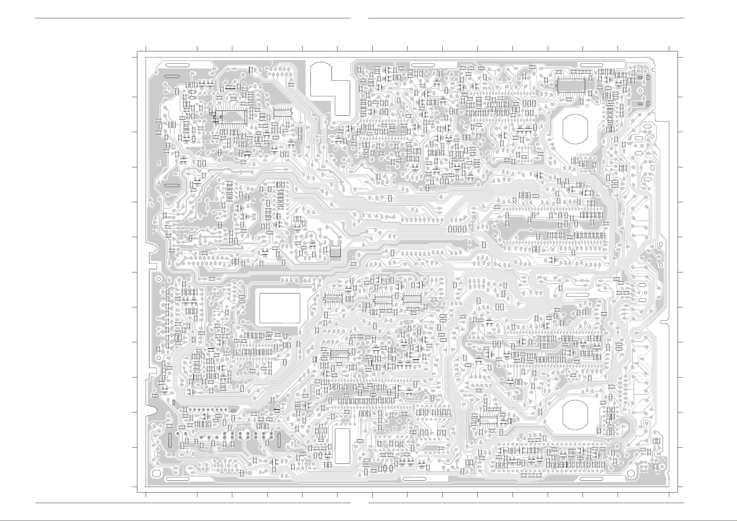
TVR 3710 …, TVR 5100 …, TVR 5500 … Platinenabbildungen und Schaltpläne / Layout of PCBs and Circuit Diagrams
8203 170 6375. 3
3103 103 39580
PSSP2
()
1234567891011121314
1234567891011121314
L
K
J
I
H
G
F
E
D
C
B
A
L
K
J
I
H
G
F
E
D
C
B
A
2246
2245
3243
3248
2886
2887
2880
2883
2884
3880
4102
4130
4222
3871
3873
3874
3875
3889
3246
3799
3839
3870
3872
2870
2885
2893 2894
7883
7884
4103
7860
7861
4105
4800
3859
3862
3877
4101
4104
4068
3854
3855
3857
3858
3848
3849
3860
3861
3899
3801
3475
3476
3490
3465
3455 3456
3419
3422
3409
3421
3415
3417
3404
3411
3492
3407
3413
2471
2427
7408
4502
3863
3864
4070
4081
4082
4501
3431
3856
3851
3528
2845
2863
3550
2512
7505
7506
2515
4096
7
112
24 13
060
3529
4503
3847
3852
3845
3846
3850
3537
3538
3815
3843
3812
3842
3844
2844
30603061
3521
3522
3545
2840
2841
2842
2843
2067
2509
2068
2066
3882
3886
3890
4027
4088
4111
6206
6209
7213
2882
2888
2890
323832393254
3881
7882
6207
7211
3897
4085
4086
4114
3267
3536
3883
3887
3888
3896
2889
2891
3226
3227
3265
7805
7709
4093
4209
4210
7206
3837
3865
3866
3867
3876
4084
3826
3828
3834
3836
3833
3827
3810
3813
3814
3817
3818
3819
3821
38033804
3808
3809
2812
2813
2816
2817
2837
2838
3892
2803
2806
2807
3820
7405
7753
3755
3800
3802
3805
3806
3807
2804
2400
3491
2405
4066
7407
4062
3457
3460
4061
3459
2404
3439
3442
3444
3445
3443
3446
3402
3406
3426
3405
3432
3401
4180
2433
3400
2071
7406
3840
3841
4007
7002 7003
3075
3424
3430
3437
3458
2428
3002
3072
2075
2073
3051
4003
4005
4006
4122
2060
2064
2069
3004
2019
2010
2013
2014
2011
2012
3232
3233
3253
3752
3884
3885
7209
7212
7260
3751
4024
4025
4026
4113
3234
3261
3262
3263
3264
3266
2210
2216
2221
2222
2262
3229
3230
7820
7210
7704
3832
4121
4131
4132
4136
4203
4230
2220
3728
7711
4120
4133
4134
4207
4208
4225
4231
3754
3891
4072
4079
2403
4139
4229
3428
3429
4063
4067
4069
7013
7020
4124
7009
7000
3039
3041
4125
3033
3038
3032
3034
30353036
3037
2049
2052
2056
2076
2117
3000
3001
3022
2043
2044
2046
2047
7015
2048
2039
2040
2045
7007
4009
4011
4015
4123
7001
3017
3018
3019
3047
40083012
3013
3014
3015
3016
2062
3003
3008
3009
3007
2028
2030
2031
2032
20332034
2021
2024
2025
2026
2000
2001
2002
2003
2006
2008
77077708
3213
3741
3746
6707
6708
7205
4098
4110
4115
4118
6210
3742
3744
3745
4019
4021
2747
3208
32093210
3211
3212
3216
3217
2741
2745
2211
2212
2213
2214
2217
2218
2205
2206
2208
2209
2215
7216
7750
7751 7752
7207
7208
7214
7215
4206
4221
4228
3756
3757
3760
4001
4058
4064
3222
3223
3228
3718
3747
3750
3753
2732
2809
2225
2226
2729
7591
7593
7502
7507
4055
4073
4094
4095
4099
4119
4204
4211
7501
3542
4051
4052
4074
2507
3540
3541
4126
4016
2054
3043
7021
7105
7106
7014
3119
3127
3128
4014
3121
3102
3116
3118
3122
3046
3045
2134
3040
3044
3042
2135
2128
2119
2124
2125
2126
2132
2121
2127
2055
2050
2051
2053
2118
7100
71017107
7016
7018
7019
7010
7005
3103
3107
3110
3117
4010
3108
3109
3048
3062
3100
3101
3023
3024
3026
3025
2104
2109
3021
2114
2106
2107
2102
2035
2036
2037
2038
2041
2042
2101
2746
3251
3770
4097
4205
6709
7710
6706
3775
4071
4107
4213
4227
3714
3719
3771
3773
3774
3200
3201
3204
3708
3713
2711
2716
2720
2730
2731
2204
2207
2708
2709
2710
2714
2201
2202
3748
7762
7703
7705
4138
4201
4226
4700
3737
4089
4108
4109
4112
4127
4137
3725
3727
3733
3734
3735
3736
3225
3240
3245
3715
3716
3720
3732
2727
2728
3219
3221
3224
2717
2718
2721
2722
2723
2725
2726
2227
2228
2248
7281
7503
7
1
16
8
9
1
16
8
9
1
16
8
9
1
16
8
9
1
16
8
9
592
4053
4075
4181
3535
3520
3524
3527
3692
4018
4054
2415
3518
3519
3523
7691
4200
7103
7104
3125
3129
4012
4013
2130
2133
3050
3124
3126
2105
2113
2115
2122
2123
2129
3106
3112
3113
3123
7102
2116
3104
3111
3105
2108
2100
2103
2110
2112
2111
7700
3203
3252
3707
4056
4224
3730
3731
3738
4002
3242
3700
3710
3711
2280
2281
2719
2750
3241
3247
2240
2249
3616
4057
4059
4128
3607
3611
3612
3615
3613
3614
3610
3525
3602
3603
3604
3605
2607
2608
2612
2613
2630
2601
2602
2604
2606
2600
2472
3691
4029
4045
4065
7490
7492
7692
4048
7403
3694
3695
3696
3697
4046
4047
3484
3488
3489
3493
3496
2691
3453
3464
3480
3481
3482
2451
2454
2458
2490
7310
7309
7311
3487
4232
4233
4301
4304
7308
3330
3332
3340
3450
3451
3454
3483
3485
3486
2432
2453
2456
3323
3324
3326
3327
2317
2318
2319
2323
2327
2070
7300
7301
4041
4044
4129
7312
4036
40374038
3348
3346
3320
3345
3325
3339
2315
3321
2314
4031
2313
4212
7250
7504
7605
7606
4090
4091
4092
4100
3659
3701
3702
3705
3706
4087
2700
2702
2703
3255
3256
3257
3258
2241
2243
2247
2256
2258
3652
2651
3601
3608
7603
3660
4060
2626
3656
3657
3658
3625
3650
3651
3653
3654
3655
3617
3620
3621
3622
3623
3624
2662
3504
3505
3544
3600
2656
2657
2658
2660
2661
2621
2652
2653
2655
2263
2502
7500 7508
3534
3619
3511
3513
3514
3516
3530
3531
3532
3533
2473
2506
2618
3471
3472
3477
2250
2261
4023
4028
7493
4022
4078
2429
2431
2457
3300
3344
4303
4020
7304
7313
6302
7282
2306
3331
4042
4043
4049
4050
4000
4039
3343
3449
4302
3318
3319
3328
3342
2307
2325
3281
3282
3283
4305
2309
4300
4035
7306 7307
6301
6300
4040
2321
3350
4030
4032
4034
2308
3351
3347
3349
4033
3315
3312
2328 23 30
2331
2332
3307
3313
2329
2304
3215
4080
4500
7509
3502
3503
3509
3543
2503
2504 2505
3500
3501
3510
3512 350 6
3507
3508
2252
2253
2254
2255
2333
3302
2303
3301
2302
3303
3304
3305
4004
18
169
1
110
20 11
14
28 15
Signal-Chassis (PSSP2)
Ansicht von der Lötseite / View of Solder Side
TVR 3710 …, TVR 5100 …, TVR 5500 … Platinenabbildungen und Schaltpläne / Layout of PCBs and Circuit Diagrams
GRUNDIG Service 4 - 41 GRUNDIG Service 4 - 42
Page 63
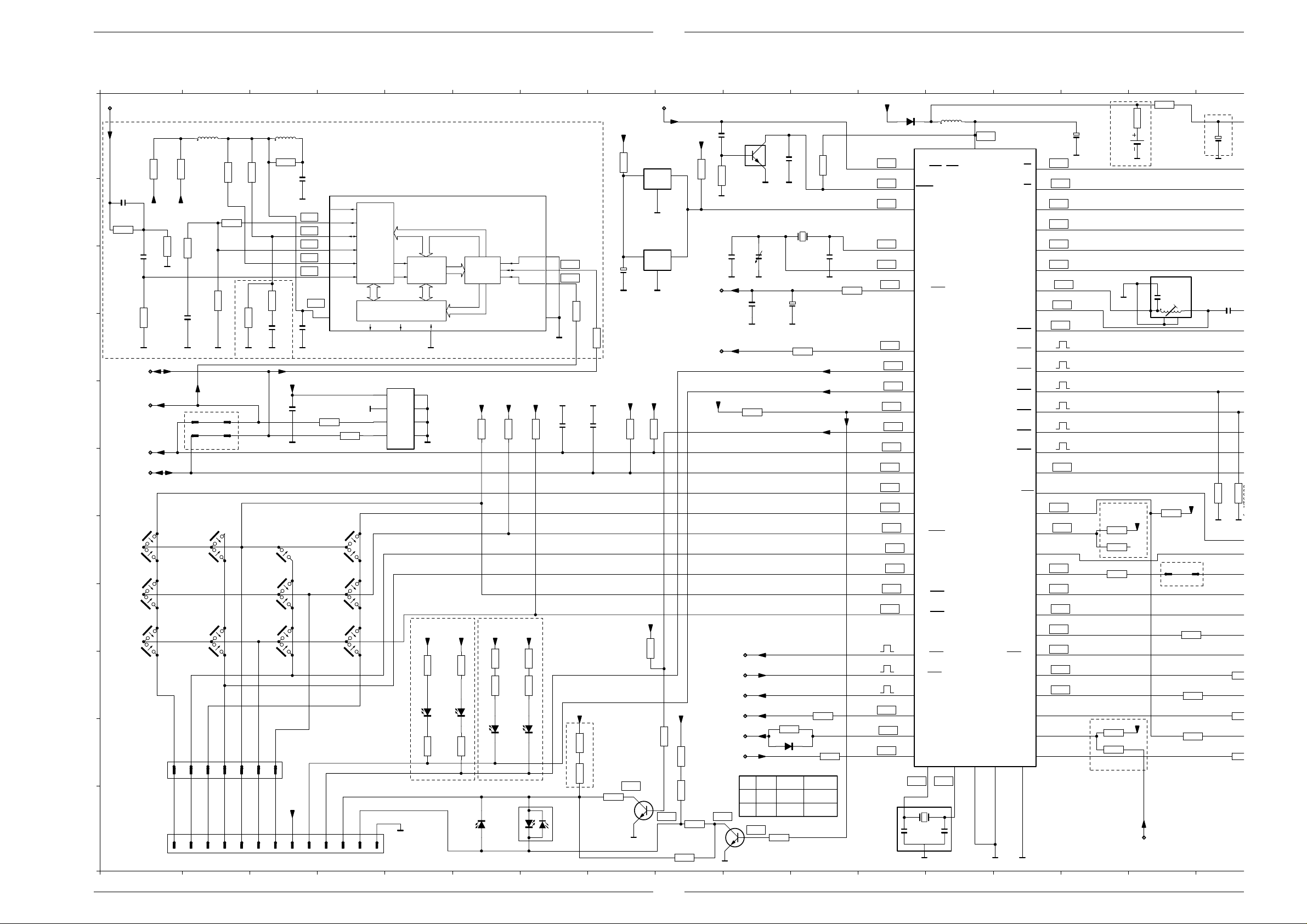
Platinenabbildungen und Schaltpläne / Layout of PCBs and Circuit Diagrams TVR 3710 …, TVR 5100 …, TVR 5500 … Platinenabbildungen und Schaltpläne / Layout of PCBs and Circuit Diagrams TVR 3710 …, TVR 5100 …, TVR 5500 …
f NTSCPB
C
d
D
0
2
2
2
Signal-Chassis – Bedieneinheit / Keyboard Control Unit (CO)
from VS
A
0E
40810E4082
for PDC only
2844
3846
3k3
5STBY 5DS
3847
100n
2843
GNDVPS
not used
B
C
1M
3845
470k for PDC
D
SDA2
to/from TU2,TV
SCL2
to TU2,TV
E
SCL
to TV,TXT
SDA
to/from TV,TXT
F
1850 1851 1853
(GRU)
G
1870 1871
1854
Pr-Up
(GRU)
H
1874
1858 1859 1860
Vol+ REC
(GRU)
1878
I
J
1908
K
1907
4561 7 8 9 101112131415161723
5840
6u8
100k
3851
delete for PDC
3850
100E
5k6
3k3
3812
8k2 for PDC
1M
3844
100n
2842
33n for PDC
GNDVPS GNDVPSGNDVPS GNDVPS GNDVPS GNDVPS
AKP
20
19 5
1502
3843
6
REWPLAY
Pr-Down
(GRU) (GRU)
1879
3
4
1
2
5
1M
3815
delete for PDC
3842
1M
2841
(GRU)
STBY
6
3852
6k8
1872
1876
1880
7
5841
GNDVPS
2n2
for PDC only
GNDVPS
5STBY
2840
VCS
5
2,8V
9
PD1
2,7V
10
INUL
2,7V
11
VCO
1,5V
12
IREF
1,2V
13
FBAS
5,2V
14 1
UDD
(GRU)(GRU)
Vol-
(GRU)(GRU)
WIND
3863
100E
DAVN EHB
3864
100E
1873
18571856
1877
1861
1881
10n
2845
2863
not used
STOP/EJECT
SDA5642 for VPS only
*
SDA5649 for VPS/PDC + time download
DATASYNC-
SLICER
CLOCK-PLL
678
8
GNDDE
7
6
5
TIMING
7813
24C08
DATA-
AQUISITION
1
2
3
4
GNDDEGNDDE
5DS 5STBY
3869
6869
3879
not used
5STBY
8
7
6
5
4
3
2
1
9
10
11
12
13
GNDDE
not used
4561 7 8 9 101112131415161723
for VPS+TU2 or PDC+TU2 only
for VPS-TXT or PDC-TXT only
7840
*
SDA5642-5
CSO
4
SDA
SCL
USS
5STBY5STBY5STBY
10k
3867
270E
270E
TIMER
TLHR4205
RED
STBY/ON
5,3V
3
5,3V
2
3841
100E
GNDVPS
100p
2837
5DS 5STBY
3853
3856
Not Used
LSG3331-JO
TI
220E
REC
TLHR4205
100E
3868
6868
3878
220E
100E
I2C-BUS
INTERFACE
10k
3865
Not used
5DS 5STBY
3849
3861
TIMER
TLHR4205
6861
6863
TLHR4205
STBY/ON
10k
3866
270E
270E
REC
TLHR4205
6862
3848
3860
6860
GREEN
3840
GNDDGNDD
2838
100E
Not Used
120E
5STBY
3835
2815
GNDDE
100E
100p
3862
0E
820E
for GRUNDIG
from DE
IR-Receiver
220E
Not Used
IR-Receiver
16V
47u
3k3
3833
2,3V
7860
BC848B
GNDD
IPORVP
7811
TFMS5360
1
GNDDE
7812
TFMS5360
1
GNDDE
5STBY5STBY
3k3
3834
5STBY
10k
3877
6k8
3857
0V
32
32
ITL
3854
3858
3855
ITR
220E
220E
330E
5STBY
3836
GRUNDIG
100E for
GRUNDIG
0E for
4800
0E
Not Used
10k
SAT
to TV
SB1_1
to TV
5STBY
2816
7805
DTC124EK
4k7
3837
GNDD
2813
DATD1
to DE
DATD2
from DE
CLKD1
to DE
CSI
to VS,TV
MES
to VS
AFC1
from TV
0,2V
GNDD
100n
not used
BC848B
3876
10k
CSI
MES
7861
2814
GNDD GNDDGNDD
2810
0,7V
7,5-50p
100n
delete
3859
10n
2817
GNDDGNDD
1803
32,768kHz
25V
2811
4u7
for NTSCPB
GNDTVGNDTV
3832
4k7
for MSTD only
3830
for MSTD only
4k7
6830
1N4148
H
HH
6k8
10k
3838
2812
10k for NTSCPB
only
for NTSCPB
STBL2
3831
100E
3829
10k
MESECAMSECAM-LPAL
LL
L
STBL1
22p
3801
100k
5STBY
5,3V
4,8V
5,3V
2,7V
1,9V
1,3V
0V
3,95V
0,2V
2,6V
0V
4,9V
4,9V
0,4V
0V
5,3V
4,9V
4,9V
5,3V
5,3V
0,3V
0V
2,7V
6801
BAT85
48
P20(INT5/STOP)
47
RESET
51
P30(INT3/RXIN)
52
P31(TC3)
50
P22(XTOUT)
49
P21(XTIN)
19
P47(PWM7)
62
P04
63
P05
28
P60
29
P61
30
P62
31
P63
55
P34(SCL/SI)
56
P35(SDA/SO)
39
P72(SCL1/SI1)
40
P73(SDA1/SO1)
41
P74(SCK1)
23
P53(AIN1)
22
P52(AIN0)
21
P51(PWM9)
20
P50(PWM8)
7
P13(DVO)
8
P14(PPG)
9
P15(TC2)
10
P16
11
P17
P54(AIN2)
2,2V 2,4V
1
1801
XTAO
8MHz
2
GNDD
XTAI
GND
5801
6u8
64
VDD
7801
T C O
TMP87SX39N
VSS
3
5V
P67(Y/BL)
P40(PWM0)
P41(PWM1)
P42(PWM2)
P43(PWM3)
P44(PWM4)
P45(PWM5)
P46(PWM6)
P32(INT4)
P36(SCK)
P10(INT0)
P11(INT1)
P12(INT2/TC1)
P57(AIN5)
P56(AIN4)
P55(AIN3)
32145 46
GNDD
P71(VD)
P70(HD)
P66(B)
P65(G)
P64(R)
OSC2
OSC1
P33(TC4)
P00
P01
P02
P03
P06
P07
44
GNDD
3800
39k
3k9
10V
2801
220u
GNDD
5,1V
38
5V
37
0V
36
0V
35
0V
34
0V
33
3,4V
43
3,4V
42
4,9V
12
13
14
15
16
17
18
53
4,7V
57
54
0V
0V
58
59
0V
60
4,8V
61
0V
2
4,8V
3
5,3V
4
0V
5
4,5V
6
27
26
2524
for VCD only
3891
1804
not used
GNDDE
GNDD
for VCD only
5STBY
3827
10k
3828
10k
3813
6k8
5STBY
3898
10k
3899
0E
3/V11H
3
2
1
3826
4k7
for TU2 and
MSTD only
21
for TU2 and MSTD or
for TU2 and SEC-DK only
for TU2 and SEC-DK or
TU2 and MSTD only
for TU2 and MSTD only
AKM
from IO
AKP
1502
07
5STBY
3822
100E
3816
3824
4
1802
6
7
2k2
4k7
GOLDCAP
5,5V
2802
220m
GNDDE
2803
27p
3808
150k
GNDD
GND
for MST
for RGB-S
4084
38
10
38
10
38
10
0E
f
4 - 43 GRUNDIG Service
4 - 44 GRUNDIG Service
Page 64
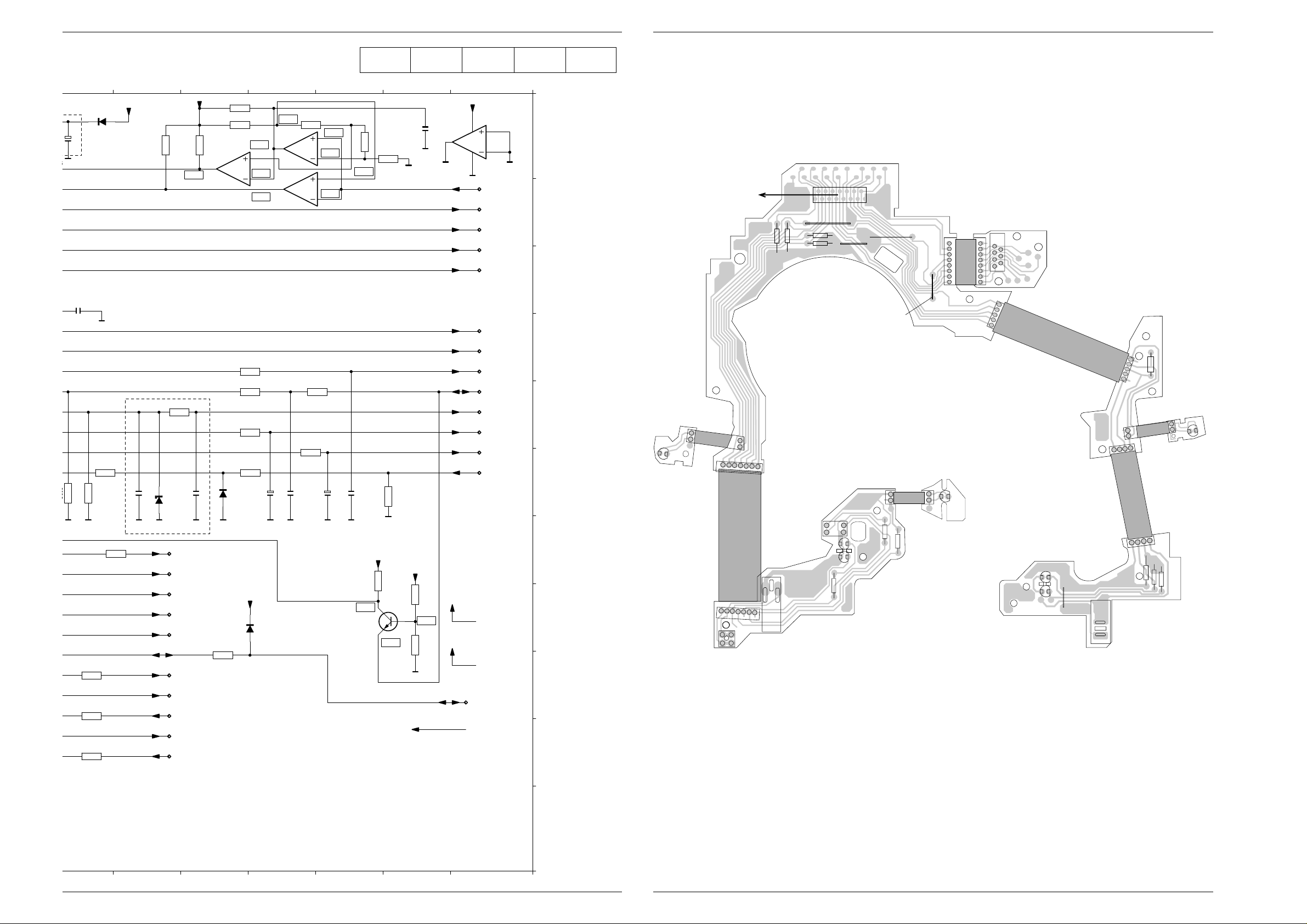
TVR 3710 …, TVR 5100 …, TVR 5500 … Platinenabbildungen und Schaltpläne / Layout of PCBs and Circuit Diagrams
y
O
3808
2802
WDSL
8203 101 75971
7105
6104
9001
SW1
RECP
3500
3502
3501
2
WTL
7102
8007
2
1
1
8006
2
0004
SW2
INIT
3600
6104
7105
7104
3601
3602
12
8005
6103
1
8004
1
2
8003
7106
3401
1
2
8002
9002
8001
1
2
3200
3300
3201
3202
9005
9004
TAE
FTA
WTR
TAS
9007
1965
1967
1
TO SIGNAL CHASSIS
DECK ELECTRONIC
CONNECTOR 1905
TVR 3710 …, TVR 5100 …, TVR 5500 … Platinenabbildungen und Schaltpläne / Layout of PCBs and Circuit Diagrams
Reference
AL ..............P 4-65
BUPI ..........P 4-68
CO .............P 4-43
DE..............P 4-49
IO...............P 4-59
OHA...........P 4-69
PLSP .........P4-19
PSSP2.......P 4-37
TU2............P 4-55
T
ube PCB
...P 4-33
TV..............P 4-51
TXT............P 4-58
VS..............P 4-61
Laufwerkplatte – Sensoreneinheit / Tape Deck Sensor Panel
17 18 19 20 21 22 23
LDCAP
NDDE
150k
NDD GNDD GNDDGNDD
r
for RGB-SCART only
6802
BAT85
5,5V
220m
2803
27p
GNDD
3809
10k
0E
4084
150k
for NTSCPB
for RGB-SCART only
delete for /08
3821
100E
for MSTD only
3823
10k
3825
10k
3814
100E
5STBY
2807
GNDD
3870
for NTSCPB
100p
6803
2k2
3805
100k
only
not used
RGBON
to TV
STBY
to TV
MONI
to TV
IMNT1
to TV
PSS2
to TU2
PSS1
to TV
MNT2
to TU2
8SC
from IO
SB1_2
to TU2
AGC1
from TV
5STBY
3871
5V
2804
2k2
13
7870
LM339N
100n
6804
3820
100E
3872
15k
3873
1k
0,3V
11
0,3V
10
5V
3802
100k
3804
100k
3806
47k
3810
10k
1N4148
5STBY
6805
2805
1N4148
2,6V
14
LM339N
1
7870
LM339N
50V
2806
2u2
100n
3839
1k5
3807
1k8
3803
100k
97870
0,8V
8
7
6
2808
GNDDGNDTV
0,8V
0,8V
16V
47u
GNDTVGNDD GNDD
2809
3874
4,2V
100n
5,2V
1k5
5STBY
3817
3875
1k
100k
3811
GNDD
10k
7820
BC848B
3,4V
GNDTV
5STBY
3818
3819
GNDD
+8V
2870
GNDTV
33k
1,3V
10k
17 18 19 20 21 22 23
GRUNDIG Service 4 - 45 GRUNDIG Service 4 - 46
4n7
2
5DS
5STBY
+8V
3
12
GNDTV
IFID
from TV
from TV
7870
LM339N
5
4
HFB/SC
from TV
BLOSD
to TV
BOSD
to TV
GOSD
to TV
ROSD
to TV
SFPOSD
to TV
IFPOSD
to TV
BRI
to TV,TXT
SHP/COIN
to TV
HUE
to TV
CONTR
to TV
VOL
to TV
PROT
from TV
from TV
from TV
GNDTVGNDTV
1502 E 2
1502 G16
1801 K12
1802 C17
1803 B11
1804 A16
A
1850 G 1
1851 G 2
1853 G 4
1854 G 1
1856 G 3
1857 G 4
1858 H 1
1859 H 2
1860 H 3
1861 H 4
1870 G 1
1871 G 2
B
1872 G 3
1873 G 4
1874 H 1
1876 H 3
1877 H 4
1878 I 1
1879 I 2
1880 I 3
1881 I 4
1907 K 1
C
1908 J 1
2801 A15
2802 A17
2803 C17
2804 F19
2805 F20
2806 F20
2807 F18
2808 F21
2809 F21
D
2810 C10
2811 C10
2812 C11
2813 C10
2814 C10
2815 C 8
2816 A 9
2817 A10
2837 E 7
2838 E 8
E
2840 B 3
2841 D 3
2842 D 2
2843 C 1
2844 B 1
2845 D 3
2863 E 3
2870 A22
3800 A16
3801 C11
F
3802 D20
3803 E21
3804 E20
3805 E18
3806 E20
3807 E20
3808 F17
3809 F17
3810 F20
3811 F21
G
3812 C 1
3813 G15
3814 G18
3815 A 2
3816 I16
3817 G21
3818 H22
3819 H22
3820 H19
3821 I17
H
3822 H16
3823 I17
3824 J16
3825 J17
3826 F16
3827 G15
3828 G15
3829 J11
3830 J10
3831 I11
I
3832 D11
3833 E 8
3834 E 8
3835 A 8
3836 A 9
3837 A 9
3838 A11
3839 A20
3840 D 8
3841 C 7
J
3842 C 3
3843 D 2
3844 C 2
3845 D 1
3846 B 1
3847 C 1
3848 I 7
3849 I 6
3850 B 2
3851 A 2
3852 A 3
K
3853 J 7
3854 J 9
3855 K 9
3856 J 7
3857 J 9
3858 K 9
3859 K10
3860 I 7
3861 I 6
3862 K 8
3863 E 4
3864 E 4
3865 E 6
3866 E 6
3867 E 7
3868 I 6
3869 I 5
3870 A18
3871 A19
3872 A19
3873 A19
3874 A21
3875 A22
3876 E10
3877 H 8
3878 J 6
3879 J 5
3891 A16
3898 J15
3899 J15
4081 A 1
4082 A 1
4084 F17
4800 K 9
5801 A13
5840 A 2
5841 A 3
6801 A12
6802 A17
6803 F18
6804 F19
6805 H19
6830 J10
6860 J 7
6861 J 6
6862 K 6
6863 K 6
6868 I 6
6869 I 5
7801 C13
7805 A10
7811 A 8
7812 B 8
7813 E 5
7820 H22
7840 B 6
7860 K 9
7861 K10
7870 A23
7870 B20
7870 A20
7870 B19
Page 65
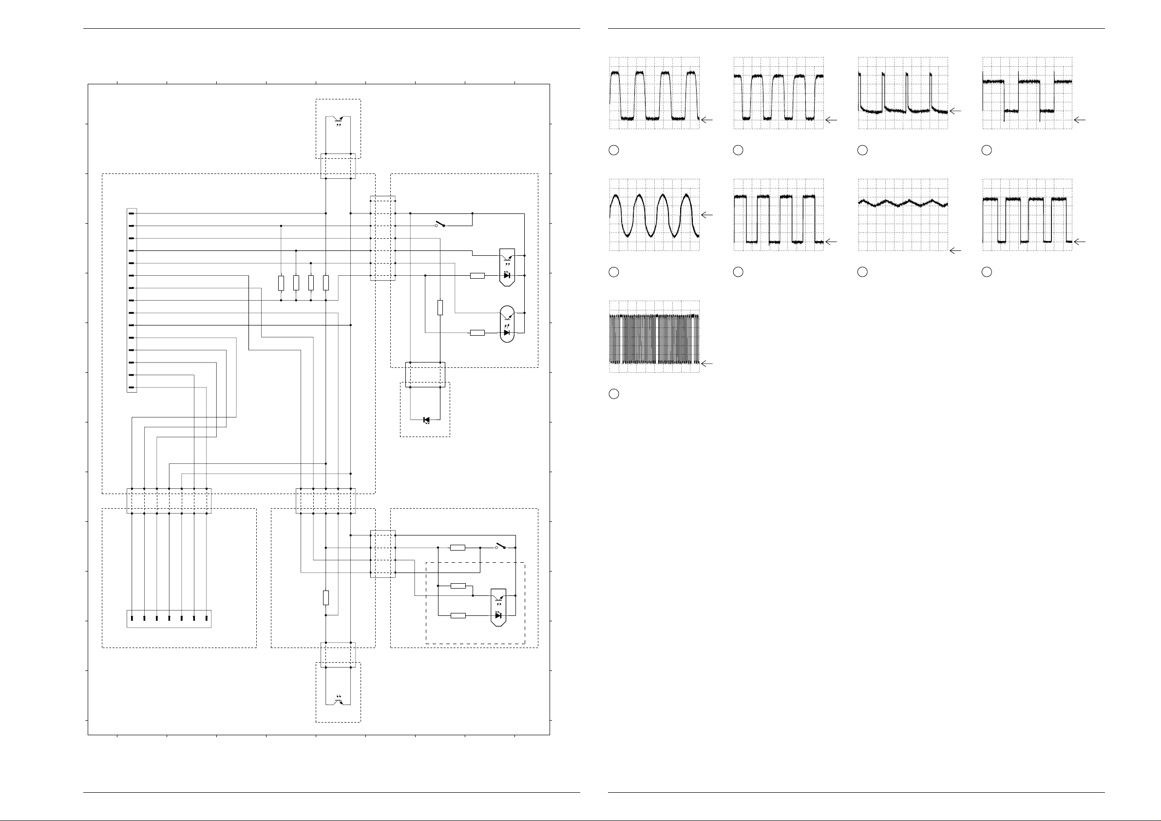
Platinenabbildungen und Schaltpläne / Layout of PCBs and Circuit Diagrams TVR 3710 …, TVR 5100 …, TVR 5500 … Platinenabbildungen und Schaltpläne / Layout of PCBs and Circuit Diagrams TVR 3710 …, TVR 5100 …, TVR 5500 …
DC, 100mV/Div, 500ms/Div
0V
Connector 1905-(9/12), IC7411-(6/7)
REC
16
DC, 1V/Div, 10ms/Div
0V
Connector 1901-(7)
REC
18
DC, 500mV/Div, 500µs/Div
2.8V
Connector 1905-(2)
REC
19
DC, 1V/Div, 10µs/Div
0V
IC7410-(31)
REC
20
DC, 1V/Div, 10µs/Div
0V
IC7410-(30)
REC
22
Laufwerkplatte – Sensoreneinheit / Tape Deck Sensor Panel
EJECT
REC
B
C
L2
TO SMALL SIGNAL BOARD 1905
D
E
F
G
1965
456789 1023
S298P
7102
TAS
24
STRIP
8007
1
3
15
TAS
14
INIT
13
LED
12
WTR
11
FTA
10
RECP
9
n.c.
8
+5D
7
TAE
6
GNDD
5
+14M1
4
CREV
3
CAP
2
FG
1
GNDM1
3202
3200
3201
15k
1K
3300
5k6
47k
STRIP
8006
1
3
5
7
9
11
13
2
4
6
8
10
12
14
4
STRIP
8005
SW21604
INIT
3601
33
13
2
3600
390
3602
390
FTA
WTR
TCRT5000
7103
TCST1030
7104
LED
V298 PB
6103
1604 C 8
1965 G 2
1967 K 2
1969 I10
3200 E 5
3201 E 5
3202 E 5
3300 E 6
3401 K 6
3500 K 8
3501 J 8
3502 K 8
3600 D 9
B
3601 E 8
3602 F 9
6103 H 8
7102 A 6
7103 D 9
7104 F 9
7105 K 9
7106 M 6
SW1 J 9
C
D
E
F
G
DC, 100mV/Div, 10ms/Div
Connector 1905-(11)
15
REC
DC, 1V/Div, 10ms/Div
Connectors 1904-(1), 1930-(6)
23
0V
0V
DC, 100mV/Div, 5ms/Div
Connector 1905-(13)
17
DC, 500mV/Div, 10µs/Div
Connector 1905-(3)
21
0V
REC
0V
H
I
J
K
L
M
STRIP
8001
CON3
1967
1357
2468
+14M1
CREV
2
1
CAP
3
+5D
4
GNDD
5
FG
6
To Capstan Motor
13119
141210
GNDM1
7
456789 1023
H
10
9
2468
STRIP
8002
1357
STRIP
8004
8
6
4
2
3501
1k
3502
27K
3500
390
OPTION
7
5
3
1
3401
68k
3
1
STRIP
8003
4
2
RECP
SW1
1502
7105
TCRT5000
WTL
I
J
K
L
TAE
M
7106
S298P
4 - 47 GRUNDIG Service
4 - 48 GRUNDIG Service
Page 66
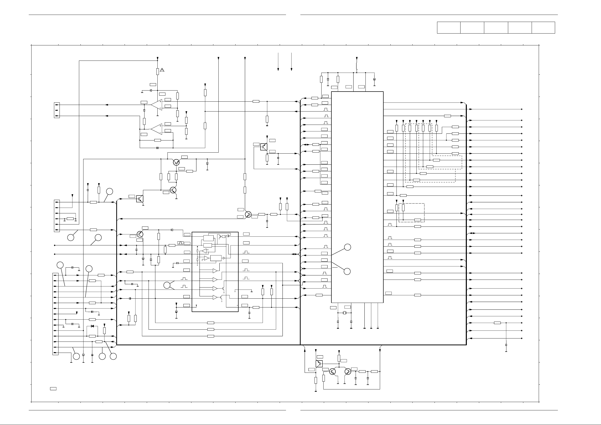
TVR 3710 …, TVR 5100 …, TVR 5500 … Platinenabbildungen und Schaltpläne / Layout of PCBs and Circuit Diagrams
Reference
AL ..............P 4-65
BUPI ..........P 4-68
CO .............P 4-43
DE..............P 4-49
IO...............P 4-59
OHA...........P 4-69
PLSP .........P4-19
PSSP2.......P 4-37
TU2............P 4-55
T
ube PCB
...P 4-33
TV..............P 4-51
TXT............P 4-58
VS..............P 4-61
Signal-Chassis – Laufwerksteuerung / Deck-Elektronik (DE)
Signal Chassis – Deck Control / Deck Electronic (DE)
TVR 3710 …, TVR 5100 …, TVR 5500 … Platinenabbildungen und Schaltpläne / Layout of PCBs and Circuit Diagrams
A
B
C
to Deck L4
D
E
F
G
H
to Headamplifier L1
I
to/from AL
to/from AL
J
K
L
M
to Deck L2 Sensor Print
N
O
1903
1
TMO1
2
NC
3
TMO2
Threading motor
1904
REEL
6
+5D
5
GNDM
4
GNDD
3
2
1
GNDDE
+14M2
PG/FG
CTL1
CTL2
17
1905
TAS
15
INIT
14
LED
13
WTR
12
FTA
11
RECP
10
WTL
9
5STBY
8
TAE
7
GNDD
6
+14/9
GNDM
GNDDE
5
CREV
4
CAP
3
FG
2
1
MEASURED IN PLAYBACK MODE...V
MEASURED IN RECORD MODE
...V
5STBY 5STBY
2429
GNDM
not used
4078
5STBY
0E
23 18
2472
10n
2473
10n
GNDM
GNDDE
5STBY
GNDDE
2470
GNDM
15
not used
25V
47u
TMO1
TMO2
not used
3456
10k
3457
1k
3471
10k
3472
22k
2457
10n
3473
1k
6401
1N4148
3477
1k2
2471
GNDDE
GNDDE
3476
4n7
3455
22k
3470
A
B
C
D
E
F
G
H
I
J
K
L
M
N
O
1400 L14
1903 C 2
1904 G 1
1905 J 1
2400 B14
2401 B16
2403 N22
2404 M15
2405 M14
2415 L 5
2427 O15
2428 O15
2429 G 3
2430 B 6
2431 C 5
2432 E 6
2433 E11
2450 H 7
2451 I 5
2452 J 5
2453 J 6
2454 J 7
2455 L 7
2456 L10
2457 L 3
2458 K 5
2470 N 3
2471 N 3
2472 J 2
2473 M 2
2490 H11
2491 F 8
3400 B13
3401 B14
3402 D19
3403 D19
3404 D19
3405 E19
3406 C13
3407 D18
3408 C19
3409 D18
3410 E19
3411 D18
3412 F18
3413 D17
3414 F18
3415 D17
3416 F18
3417 D17
3418 G17
3419 D17
3420 G17
3421 H17
3422 H18
3423 I18
3424 I18
3425 J18
3426 J18
3427 K18
3428 K18
3429 M21
3430 O16
3431 O15
3432 O13
3433 H13
3434 H18
3435 G13
3436 G13
3437 O13
3438 F13
3439 E13
3440 E13
3441 E19
3442 C13
3443 E11
3444 D11
3445 C10
3446 B 8
3447 D 8
3448 D 7
3449 D 7
3450 B 7
3451 C 7
3452 A 6
3453 D 5
3454 D 6
3455 G 3
3456 G 3
3457 H 3
3458 N14
3459 G12
3460 H11
3461 G11
3462 G10
3463 F10
3464 H11
3465 H17
3470 K 3
3471 K 3
3472 L 3
3473 M 3
3475 M 3
3476 N 3
3477 M 3
3478 K13
3480 I 6
3481 I 7
3482 I 6
3483 J 6
3484 J 5
3485 M 4
3486 M 5
3487 M 8
3488 M 8
3489 M 8
3490 L10
3491 K11
3492 K11
3493 F 7
3494 F 7
3495 F 6
3496 F 6
4078 H 2
5401 A15
6401 M 3
7402 C 6
7402 D 6
7403 H 5
7405 E11
7406 N13
7407 O14
7408 O15
7410 F15
7411 L 8
7490 H10
7491 F 6
7492 G 7
7493 G 6
4561 7 8 9 10 11 12 13 14 15 16 172 18 19 20 21 223
from TV
+14/9M1+14M2 +14M1
2E2
3452
14.65V
14.5V
2430
25V
47u
GNDM
14V
13V
2431
3453
14V
13V
1k8
22
REEL
PG/FG
TAS
1k
LED
WTR
FTA
I/R
WTL
TAE
5STBY
2k2
3475
CREV
IWIND
LED
IWIND
CTL1
CTL2
FTA
WTR
WTL
FG
WTLD
3484
10k
2415
100n
5STBY
3485
3,2V
7403
BC848B
3.2V
2458
10n
2k2
2451
GNDDE
3486
GNDDE
2.5V
2.5V
4n7
2452
GNDDE
100k
7402
1
L2722
100n
7402
1E5
L2722
3
7493
DTC124EK
16V
2453
100u
13.6V
7
2
8
4
GNDM
6
5
3454
82k
2432
10n
10k
3496
470E
3480
1n
3483
39k
3482
5.3V
2.2V
3.6V
2.8V
0V
7491
BD438
3495
47u
4k7
680E
2450
3481
220E
GNDDE
16V
3450
3451
GNDM
680E
3494
7492
BC848B
GNDDE
2454
33n
22k
3k9
14.3V
14.3V
5STBY
10k
3448
3449
22k
GNDDE
3493
2.5V
2.5V
2.5V
2.1V
3.2V
16
2.5V
5STBY
16V
2455
47u
GNDDE GNDDE
CAP
5STBY
2k2
3446
22k
3447
25V
2491
1k
47u
GNDM
13.5V
0.6V
DECK INTERFACE
CTL_FB
1
- AMPLIFIER
- FILTER
- DETECTOR
CTL_IN/OUT
2
WRITE
AMPLIFIER
+
Vref
-
VREF
3
PO/FC
4
COMP1_IN
5
COMP2_IN
6
COMP3_IN
7
COMP4_IN
811
VCC
9
Vref
+
-
7411
SAA1310
3487
2M2
3488
100k
3489
100k
POWER-ON AND
POWER-FAIL
DETECTOR
+
+
+
-
+
-
CAP_REV
PO/F_OUT
CTL_DATA
COMP1_OUT
COMP2_OUT
COMP3_OUT
GND
COMP4_OUT
W/R
3445
10k
10k
3444
GNDDE
5STBY
7405
DTA124EK
4k7
3443
GNDDE
3464
220E
2490
GNDDE
5STBY 5STBY
4k7
3491
5,2V
0,1V
3460
4n7
3492
5,2V
68E
3463
68E
3462
BC848B
7490
0.5V
5,2V
18
0.1V
0.11V
17
16
4,9V
15
14
13
12
GNDDE
2.6V
3490
5.3V5.3V
10
2456
4k7
100n
FG
2021 19
from TV
from TVfrom TVfrom TV
5STBY5DS
4k7
3400
3442
IREC
TMO
THIO
LPA
for LP only
3406
1k2
1k
SYNC
WTLD
2433
GNDDE
PG/FG
FGD
CKPAL
IPOR
10n
IWIND
TAS
POR
I/R
TAE
3439
10k
3440
3438
2,9V
2,6V
2V
5V
1k
5,2V
1,6V
10k
5,2V
2V
3435
TRIV
1k
3436
10k
for TU2 only
3433
1k
2,4V
2,8V
5STBY
5DS
12k
4k7
3459
3461
1k
LEDD
AFC2
CLKD1
CREV
CSYNC1
ENVC
VISS
POR
SYNC
WTRD
WTLD
DATD1
DATD2
REEL
CAP
IPOR
SYNC
FTAD
3,1V
2,6V
5,3V
4,9V
WTRD
4k7
FGD
ISON
3478
10k
W/R
5DS
5V
7406
DTA124EK
CSYNC1
10k
3432
GNDDE
0,3V0,7V
3437
10k
3401
100n
2400
5,2V
GNDDE
21 64 62
TEST
0V
9
P30
0V
10
P31
16
P37
PWM8
17
P64
CAP0
15
INT1
P36
18
P65
CAP1
19
P66
CAP2
52
P61
AN11
51
P62
AN12
54
P57
AN07
55
P56
AN06
56
P55
AN05
57
P54
AN04
58
P53
AN03
59
P52
AN02
60
P51
AN01
61
P50
AN00
1
P40
SCLK0
0V
44
P13
TPG0-11/TPG1-11
12
P33
C-SYNC
13
P34
EXT
3
P42
RXD0
2
P41
TXD0
30
PW0
31
PW1
46
RESET
20
P67
CAP3
7
P46
INT2
14
P35
INT0
8
P47
TI1
XTAL2
2,3V
2405
GNDDE GNDDE
5DS
3458
7407
BC848B
1k
GNDDEGNDDE
Compositesync-Integration
5STBY
6u8
5401
5,3V 5,3V
VCC1
7410
T V C
TMP91C642AN
22
20
XTAL1
CLK
2,1V
1400
10MHz
22p
22p
2404
GNDDE GNDDE GNDDE
4k7
4,4V
7408
BC848B
0,4V
3431
4k7
10n
2427
GNDDE GNDDE
2401
GNDDE
VREF
AN10
AN13
TPG0-10/TPG1-10
TPG0-9/TPG1-9
TPG0-8/TPG1-8
TPG1-0
TPG1-1
TPG1-2
TPG1-3
TPG1-4
TPG1-5
TPG1-6
TPG1-7
TPG0-7
TPG0-6
TPG0-5
TPG0-4
TPG0-3
TPG0-2
TPG0-1
TPG0-0
RXD1
TXD1
SCLK1
VSS2
VSS1
32 494748
3430
0E
2428
not used
AGND
6345
16V
47u
P60
P63
P12
P11
P10
P20
P21
P22
P23
P24
P25
P26
P27
P07
P06
P05
P04
P03
P02
P01
P00
P32
P45
P44
P43
CSYNC
3408
TMO
FMSW
VISS
1k
3402
1k
3403
4k7
3404
1k
3441
4k7
3405
1k
LPA
DO
IPAL
IPBV
MTA
ITRICK
VS1
VS2
OS2
OS1
RS1
RS2
ENVC
CSYNC
W/R
TRIV
HSC2
HP1
CKPAL
CROT
HSC
FFP
SYNC
FMSW
to VS
LPA
to AL
DO
to VS
IPAL
to AL
IPBV
to VS
MTA
to AL,TU2
ITRICK
to VS
VS1
to IO
VS2
to IO
OS2
to IO
OS1
to IO
RS1
to IO
RS2
to IO
ENVC
from VS
CSYNC
from VS
TRIV
from VS
HSC2
to VS
HP1
to VS
CKPAL
from/to VS
CROT
to VS
HSC
to VS
FFP
to VS
LEDD
I/E
LPV
ISON
INTSC
AFC2
IREC
DATD1
DATD2
IPOR
CLKD1
3429
100E
2403
GNDDE
180p
I/E
to TV
LPV
to VS
ISON
to IO
INTSC
to VS,TV
AFC2
from TU2
IREC
to AL,VS
DATD1
from CO
DATD2
to CO
IPOR
to CO
CLKD1
from CO
53
50
43
42
41
40
39
38
37
36
35
34
33
29
28
27
26
25
24
23
22
11
6
5
4
5STBY5STBY 5STBY
5STBY 5STBY 5STBY 5STBY
10k
10k
3417
3419
5,2V
3415
5,2V
0V
5,2V
5,2V
5STBY
3421
3418
100k
3420
100k
5STBY
4k7
3465
0V
0V
5,2V
0V
5,1V
5,2V
10k
10k
3413
3411
3414
100k
for SCART Output Select only
3416
100k
not used
3434
3422
12k
3423
33k
3424
8k2
3425
6k8
3426
10k
3427
1k
3428
1k
for NTSCPB only
10k
3409
3412
100k
10k
10k
3407
3410
100k
for View Select only
4561 7 8 9 10 11 12 13 14 15 16 172 18 19 20 21 223
GRUNDIG Service 4 - 49 GRUNDIG Service 4 - 50
Page 67
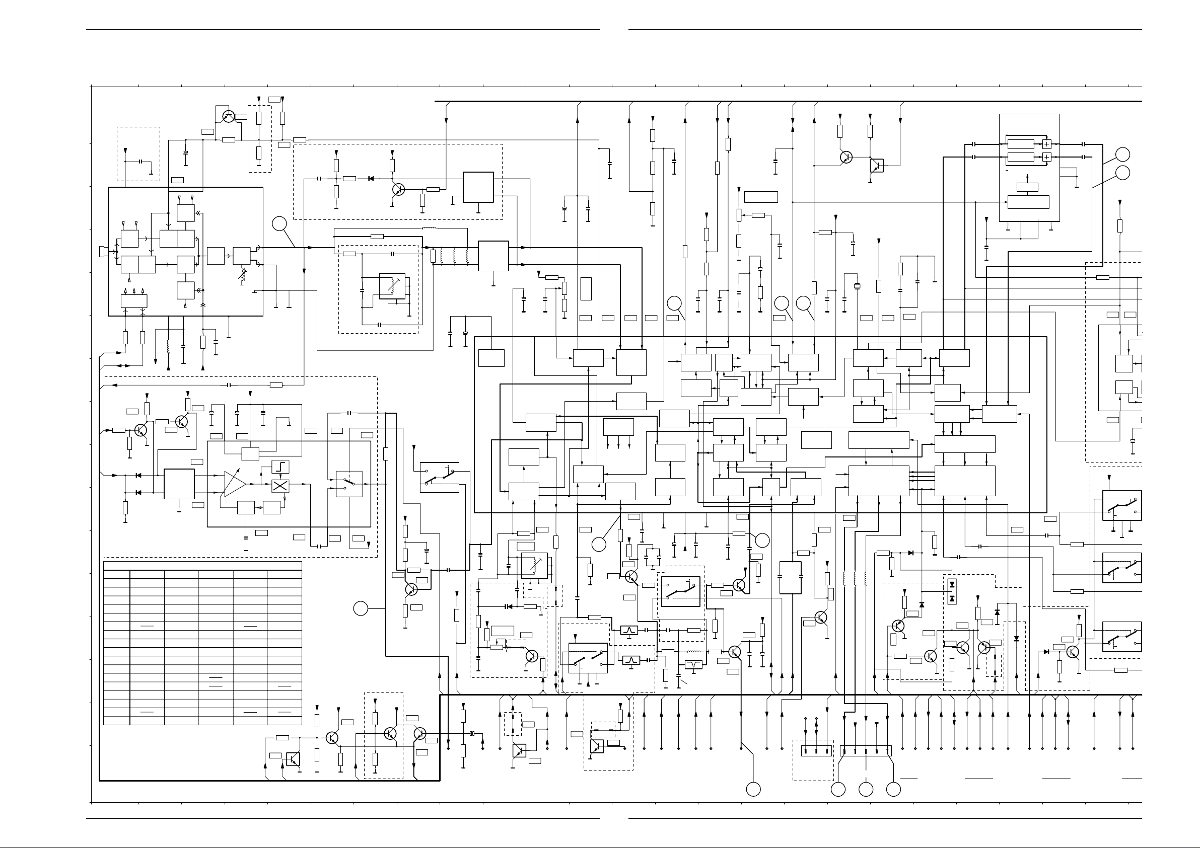
Platinenabbildungen und Schaltpläne / Layout of PCBs and Circuit Diagrams TVR 3710 …, TVR 5100 …, TVR 5500 … Platinenabbildungen und Schaltpläne / Layout of PCBs and Circuit Diagrams TVR 3710 …, TVR 5100 …, TVR 5500 …
IFID
D
n
Signal-Chassis – TV-Signalelektronik / TV Signal Electronics (TV)
4561 7 8 9 10 11 12 13 14 15 16 17 182 19 20 21 22 23 243
+12A
4,7V
12k
3701
33k
3702
for PAL-I only
30
IF
17
17
16
16
MT
GNDTV
4056
0E
22n
2745
AGC
Detector
TDA9830/V1
2,3V
25V
4u7
TRAP 5,5/6,5MHz
BP 5,5MHz
BP 6,5MHz
4,9V
SFPOSD
5AS2
10k
3706
delete for PAL-I
3707
1k8
2,17V
GNDAM
1314
567
2,15V
G1966M
820E
120E
0E
5u6
TDA8362TDA8362 TDA8361TDA8361
3755
56k
7753
DTC124EK
GNDD GNDTV
IFPOSD
+8V +8V
3k3
3775
3773
2750
2741
220n
+8V
3753
3754
GNDD
1n
10k
7752
BC848B
10k
4k7
3k3
3774
GNDTV
3708
100E
40,4MHz
TRAP1
for MSTD
only
2747
220n
2,2V4,86V
9
1
0
2,2V 4,86V
+8V
8V
1k
3750
delete for MSTD
2708
4,86V
1011
12
32
STTV
6709
BA582
not used
5AS1
4071
0E
6
4
2710
120p
8
+8V
7751
100k
3752
BC848B
100k
3751
GNDTV
1k
3770
BF570
GNDTV
2709
220p
5704
41859
07
0E
4021
delete for MSTD
6,2V
7,7V
7703
BC848C
+8V
for TXT
only
7710
3771
GNDTV
not used
3
2
1
GNDTV
*TDA8362/N5
+8V
1
Y1
2
Y0
for SEC-DK or MSTD only
+12A
3740
270E
3738
820E
3737
GNDTV
470k
1,8V
1,8V
1,1V
1,2V
3736
220E
GNDTV
8V
BC848B
1,4V
VEXT
MNT1
for SEC-DK only
3772
3k3
3k3
GNDTV
5703
EL0405
3719
5701
1u
3719
not used
delete for MSTD
2711
GNDTV
for SECAM only
7705
HEF4053BT
E
16V
2740
47u
2717
220n
PSS1
7750
2V
AFV1
1
2
EL0606
5702
1u
for MSTD only
100n
2712
GNDTV
5707
1732
L9360M
3
GNDTV
TRAP
5707
not used
50V
2u2
5
4
2715
GNDTV
1
1720
5
*
2
3
GNDTV
4
+8V
3711
5k6
10k
100n
2714
1k5
3710
GNDTV GNDTV
GNDTV
2713
GNDTV
16V
10u
505152
Supply IF
7200
*
TDA8361/N5
Preampl.
Mute
Video
Identifier
Z
15
S
+8V
3734
IPSS1
to IO
10
4k7
+8V
3757
3756
GNDTV
H = SECAM
L = PAL
2718
GNDTV
2720
3731
for MSTD only
2719
GNDTV
47k
2748
16V
10u
15k
100k
10n
+8V
3730
10n
VTV
3n9
18k
from IO
Demodulator
100p
2721
2722
6706
BBY40
for MSTD only
L'-ADJ1
AKP
18
4k7
1502
3729
IPSS1
INTSC
15
AKP
3
INTSC
from DE
GNDD
2
3733
6k8
AFC1
6
4
07
10n
GNDTV
3732
10k
8V
1
BC848B
GNDD
PSS1
4,9V
1502
DTC124EK
7709
0V
for MSTD only
3
7,4V
5705
GNDTV
7704
SB1_1
3728
3
2
1
100k
PSS1
4
100k
3727
16
AKP
1502
4
for SEC-DK or MSTD only
S
11
Z
14
IFID
MNT1
ATV
ATV
from CO
AGC1
50V
2u2
3712
10n
2731
GNDTV
AGC1
AGC
2730
GNDTV
Power
Reset
100n
Amplifier
AFC and
Sample-
and Hold
PWR2PWR1
AFC1
PWR3
Switch
Volume
Video
Amplifier
*
Y0
Y1
AKP
1502
DTC124EK
7711
3,2V
12
13
17
3,5V
2725
+8V
470E
3716
3735
150E
7V
7762
for MSTD
BFS19
2,6V
1745
*
3
1
2
GNDTV
1746
*
1
2
GNDTV
+8V
MNT1
2k2
3748
0V
IMNT1
from CO
5 7 8 9
3V
31
1k
3725
GNDTV
1n
2723
4700
0E
+8V
7705
Vdd
HEF4053BT
Vss
E
Vee
61678
GNDTVGNDTV
-7V
2
8V
GNDD
from IO
+8V
39k
3713
15k
3714
27k
3715
GNDTV
PWR1
Detector
PLL
Limiter
GNDTV
100n
GNDTV
16V
2733
2726
100n
10u
GNDTV
3720
22E
3
Y1
only
5
Y0
for SEC-DK or MSTD only
2727
2732
47p
220p
3718
2728
3
47p
3747
GNDTV
BLUE
BLSC
BLSC
BLUE
from IO
3213
1k
8V
7205
BC848B
1,4V
5STBY
3k9
3214
7206
DTC124EK
GNDD
MONI
2210
2211
1,4V
1n
1n
1,4V
2716
GNDTV
100n
VDR
VCOMP
2M2
3203
3204
VFB
+8V
HDR
HFB/SC
0E
2207
not used
+8V
GNDTV
21mV
H-SHIFT
+33V
180k
3202
100E
3200
2%
3M3
3201
2201
100n
2200
43
GNDTV
Output
Divider
GNDTV
Coincidenz
Detector
H AND V
4,2V4,3V4,3V1,7V3V
Vertikal
Vertikal
Noise
Chrominance
Switch
Trap and
Bypass
Tuning
10 11 12 13 14 15 16 17 18 191 20 21 22 23 24 25 26
GNDTV
16V
22n
2228
2229
47u
+8V
7705
HEF4053BT
*
2729
560E
GNDTV
GREEN
from IO
GNDTVGNDTV
E
3760
680E
5706
1740
3
2
GNDTV
100p
for MSTD only
GREEN
from IO
RED
Z
S
*
RED
4
9
*
1
from IO
3220
1k
*
3222
GNDTV
4201
0E
BRI
BRI
from CO,TXT
GNDTV
1,9V
*
2V
10n
SEP.
10k
3206
0E
3215
GNDTV
2202
3207
470k
2203
2n2
3208
GNDTV
40414243444546474849
Phase 1
Line
Oscillator
Amplifier
2n2
2204
GNDTV
50V
1u
22k
33
34
Phase 2
Tuning
ACC
PWR3
3209
680E
3210
8k2
2205
GNDTV
+8V
100n
2206
GNDTV
2230
not used
GNDTV
1200
18p
Oscillator
System
Manager
Colour
Killers
4,433664MHz
XTal-
Test
Chrominance
Bandpass
PWR2
Luminance
Y-Delay
Peaking
3,7V
5,3V 2,5V 3,8V 7,7V 1,7V 1,8V 1,8V 1,8V 0,3V
3219
2M2
for MSTD
only
42
220n
2227
47n
2226
1,3V
+8V
5k6
3221
7216
BC848B
GNDTV
+8V
150E
3223
7,9V
BC848B
7215
100n
2225
2224
GNDTV
GNDTV
1,2V
AGC1
VFV1
to IO
2223
16V
10u
IPSS1
SHP/COIN
AGC1
to CO
220n
for PAL-I only
VEXT
I/E
from DE
Switch
3224
2M2
2231
0V
0,7V
SCL2
1
1973
75mV
470E
3228
+8V
47n
3225
delete for PAL-I
7,8V
7214
BC848B
GNDTV
from CO
from/to CO
SDA2
3
2
SCL
SDA
2k2
39mV
BRI
STBY
STBY
for VCD only
40
38 3937
Output
Stages
2,2V
6u8
6u8
6u8
5203
5202
5201
BRG
+8V
345
1
2
1913
R
G
+8V
to TUBE-PCB 1967
+8V
8k2
3211
3,6V2,6V3,8V
PWL
3226
2k2
BLOSD
BLTXT
GNDTV
GNDTV
3227
GNDTXT
7213
BC858B
0V
3230
B
100k
3212
100n
2208
5V
Phase
Detector
6207
BAS16
delete for
RGB-SCART
not used
5DDA
1k
3229
0,7V
for TXT only
GNDTXT
4k7
0V
RGBON
SB1_1
SB1_1
4n7
2209
GNDTV
1n for NTSCPB
3253
GNDTXT
6209
BAS16
0,7V
7212
PMBT2369
GNDTXT
PROT
PROT
RGBON
from/to CO
Demodulator
HUE
Control
Matrix
Luminance
1k
PMBT2369
0V
3267
SCL
SCL
Matrix
Clamp-
Switch
2222
100n
6206
BAV70
0,7V
7211
4k7
GNDD
SDA
SDA
30313233343536373839
RGBON
HFB/SC
HFB/SC
2221
100n
5DDA
1k
3266
7210
BC858B
GNDD
SFPOSD
5AS1
2214
GNDTV
0,7V
SFPOSD
+(R-Y)comb filtering
16
14
+(B-Y)comb filtering
5
GND
10
10n
3,9V1,5V1,5V1,6V4,3V2,5V8V 2V1V0,8V2,8V3,8V2,4V2,7V3,8V5,4V4V4V9,0V1,3V2,0V4,4V6,6V
Clamps
Set
6210
BAT54
GNDTV
0V
22
AKP
1502
14
BLSC
IFPOSD
IFPOSD
from/to CO
7201
TDA4665/V4
LINE DELAY
LINE DELAY
VCO
LINE-LOCKED PLL /
PULSE PROCESSING
Vp1
123
9
5,1V
3,9V 5,8V
272829
1,7V2,4V3,4V3,4V3,4V2,8V8V1,7V4,7V2,5V5,8V5,8V3V
3,65V
2220
100n
6200
1N4148
6208
1N4148
BCI
RGBON
HUE
SAT
CONTR
HUE
GND
GND
i.c.
n.c.
n.c.
n.c.
n.c.
GNDVp2
GNDTVGNDTV
1,3V
7209
PMBT2369
VOL
0,2V
3265
GNDD
VOL
3V
11
12
3V
4
8
7
GNDTV
6
13
15
4024
delete for
RGB-SCART
4025
delete for
RGB-SCART
5V
2k2
SHP/COIN
SHP/COIN
2212
100n
2213
100n
3218
10k
5,8V
Video
11
14
0E
10
15
0E
5DS
9
1k
3264
4
GNDD
MONI
MONI
from/to CO
+8V
3217
6V 0,8V
fsc
12
1,6V
5DS
Vdd
HC4053
S
Z
E
61678
HC4053
S
Z
E
HC4053
S
Z
E
delete for
RGB-SCART
35
36
10k
delete for NTSCPB
0,8V
1516
T
ACC
Interf.
2219
GNDTV
7260
Vss
Vee
GNDDGNDD
GNDTV
7260
7260
4026
0E
STBY
AFC1
AFC1
2700
10n
GNDTV
PIN 5 for UV916S
PIN 9 for UV1216D
56
AGC
A
for PAL-I only
delete for TU2
+12A
B
VCC2
C
III
I
III
I
BPF
BPF
RF
D
BPF
BPF
E
F
G
H
I
J
K
L
SCL
SDA
IF
SB1_1
IF
Pos.
1701
1740
1745
1746
3743
47k
CL
GNDAM
PLL
PLL
3703
GNDAM
3741
100E
2,7V
7707
BC848B
3742
4k7
AGC
AGC
AGC
AGC
U
IIIUI
U
IIIUI
VCC1
DA
12 8
3704
100E
5700
5AS2
5AS
5AS1
4k7
3744
3746
100k
0,63V
100k
GNDAM
6707
1
BA582
6708
2
BA582
for MSTD only
PAL-BG MSTD PAL-I P/S-DK
UV916S
G1966M1720
TRAP 5,5MHz
BP 5,5MHz BP 5,5MHz
M
1k2 820E
3222
3718
4201
N
4700
5706
7200
7754 TDA9830
0E
0E 0E
15u 5u6
O
P
7700
BC848B
2,1V
3700
12k
16V
2701
47u
GNDTV GNDTV
4,7V
9
IIIUI
IIIUI
1701
*
UV916S
1702
UV1216D/P
for Tuner 2 only
AMP
AMP
BPF
BPF
CS
50V
GNDTV
22k
2703
3705
100n
4k7
3745
GNDAM
100n
GNDTV
+33V
2746
100p
75mV
25V
2743
2744
4u7
GNDTV GNDTV GNDTV GNDTV
4,86V4,37V
4
15
7754
1,7V
16
4
1
5
1,7V
23
UV916S UV916S
G1965M G1965M
TRAP 5,5/6,0MHz
BP 6,0MHz
100E270E
6u8
7708
BC848B
1750
L9453M
3
GNDAM
*
VCO
VCO
MIX
MIX
MIX
MIX
VCO
VCO
2702
GNDTV
VERSION
2,1V
101113 14 15
5AS15AS1
16V
10u
Supply
bandgap
AGC
Control
2742
GNDTV
U944IEC
TRAP 6,0MHz
BP 6,0MHz
2k7
270E
0E
15u
4561 7 8 9 10 11 12 13 14 15 16 17 182 19 20 21 22 23 243
Sa
16V
47u
Y0
Y1
Y0
Y1
Y0
Y1
STBY
4 - 51 GRUNDIG Service
4 - 52 GRUNDIG Service
Page 68
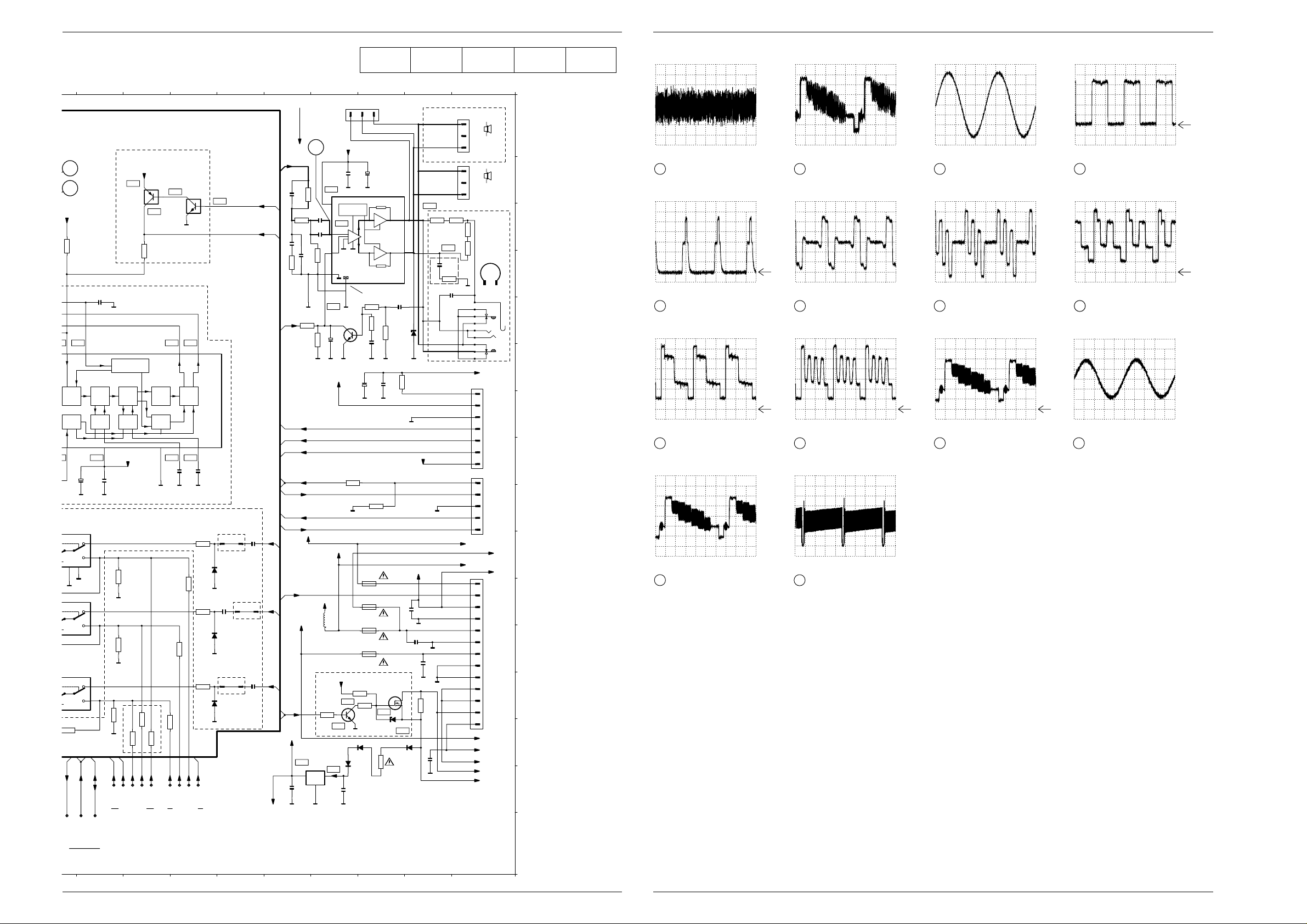
TVR 3710 …, TVR 5100 …, TVR 5500 … Platinenabbildungen und Schaltpläne / Layout of PCBs and Circuit Diagrams
AC, 200mV/Div, 20ms/Div
Tuner 1701/1702-(17)
TV
30
DC, 500mV/Div, 20µs/Div
0V
IC7200-(37), Connector 1922-(4)
TV
33
DC, 1V/Div, 20µs/Div
0V
IC7200-(38), Connector 1922-(5)
TV
34
DC, 500mV/Div, 20µs/Div
0V
IC7200-(20)
TV
37
DC, 500mV/Div, 20µs/Div
0V
IC7200-(19)
TV
38
DC, 500mV/Div, 10µs/Div
IC7200-(13)
TV
42
AFC1
3217
6
TVR 3710 …, TVR 5100 …, TVR 5500 … Platinenabbildungen und Schaltpläne / Layout of PCBs and Circuit Diagrams
35
36
+8V
10k
delete for NTSCPB
12 345678
HC4053
D
HC4053
HC4053
lete for
GRUNDIG Service 4 - 53 GRUNDIG Service 4 - 54
2215
47p
0,8V
0,8V 1,5V 1,5V
Sandcastle
TDA8395P/N2
Cloche
ACC
Interf.
Tunning
8V
16V
2219
47u
GNDTV GNDTV
7260
Y0
12
Y1
13
Vee Vss
78
GNDD
GNDTV
7260
Y0
2
Y1
1
7260
Y0
5
Y1
3
4026
0E
B-SCART
STBY
IFID
IFID
STBY
AFC1
for NTSCPB only
+8V
7207
8V
DTA124EK
8V
10k
3216
for SECAM only
GNDTV
Control
PLL
Tunning
Ident
+8V
10n
2218
for RGB-SCART only
1k
3232
1k5 forTXT
GNDTV
1k
3233
1k5 forTXT
GNDTV
1k
3234
GNDTV
3k3
3238
1k5 forTXT
3k3
3254
3239
STTV
GTXT
RTXT
BLTXT
from TXT from CO
7208
0V
DTC124EK
GNDTV
1,5V
9
101112131415
-(R-Y) -(B-Y)
Output
Deemph.
Stage
4V3,3V
2216
100n
2217
GNDTV GNDTV GNDTV
8k2
3235
12k
3236
12k
3237
for TXT only
3k3
ROSD
GOSD
BTXT
BOSD
1,5V
7202
3261
1k
3262
1k
3263
1k
BLOSD
220n
6261
GNDTV
6262
GNDTV
6263
GNDTV
5V
27
BAT85
2262
100n
BAT85
28
BAT85
AKP
1502
AKP
1502
Reference
AL ..............P 4-65
BUPI ..........P 4-68
CO .............P 4-43
DE..............P 4-49
IO...............P 4-59
OHA...........P 4-69
PLSP .........P4-19
PSSP2.......P 4-37
32 3325 26 27 28 29 30 31
from AL
+12A
ATV
10n
2248
2249
3241
VOL
VCOMP
BCI
PROT
HFB/SC
HDR
VFB
VDR
STBY
STBY
+8V
2281
4k7
3247
8k2
100n
2240
5DS
8V
100n
3
3240
GNDTV
3245
4k7
5STBY
L78M08CV
INTSC
HUE
BLUE
2261
11
100n
AKP
GREEN
23
12
1502
RED
2263
13
100n
+8V
to CO
41
4k7
2247
220n
2243
220n
5n6
22k
3255
2k7
3242
GNDTVGNDTV
5AS1
7280
2
for Plug Print only
1971
1
+9VA
220n
2241
11,7V
GND9VA
VCC
2
Protection
2,4V
INPUT
+
3
-
5
DC_VOL_CONTR
GND
4
POWER-GND
7
0,8V
GND9VA
16V
7250
2244
47u
BC848B
GNDTV
+9VA
3251
10k
GNDTV
5AS
22u
5200
FOR LOW POWER STBY ONLY
+33V
3281
220k
26,5V
3283
47k
0V
GNDT
1N4001
6202
1N4001
11V
1
2280
100n
GNDTVGNDTV GNDTV
2
3
25V
2242
680u
7240
GND9VA
TDA7056B
NC1
19
cooling plate
3256
33k
10k
3257
56k
3258
2258
220n
GNDTV
16V
10n
2250
2251
100u
GNDTV
GNDTV
3252
1k
1004
T250mA
for TU2 only
1003
T500mA
1002
T630mA
1001
T500mA
7281
STD17N06
3282
1k
26,5V
7282
BC847B
6280
BZX79-C12
6203
2E2
3270
OUT(+)
OUT(-)
NC3
2256
220n
3250
14V
6
8
6242
BZX79-C18
GNDTVGNDTV
100E
GND9VA
+33V
2253
100n
GNDA
2252
100n
GNDA
4200
6205
1N4001
+8V
2254
0E
for 2 speakers only
1
2
3
1970
1
2
3
3243
47E
5,6V
not
2245
used
3246
2246
22n
GNDTV
GNDD
220n
GNDM
delete for
LOW POWER STBY
2255
220n
3248
47E
1914
3249
3244
GNDTXT
LGS6507
1
2
3
4
5
6
7
8
9
10
11
12
13
1
2
3
4
5
6
7
1
2
3
4
5
5STBY
to CO,DE
to VS,IO
5,6V
GNDA
LS1
N.C.
LS2
LS1
N.C.
LS2
delete for
47E
Plug Print
47E
32 Ohm
1916
1
9
8
7
2
3
4
5
6
1912
1911
5AS
1909
16 Ohm
-7V
to IO,AL
5DS
to DE,CO,TXT
+14/9M1
to DE
+14M2
to DE
+14M1
to DE
+14M1S
to AL
32 3325 26 27 28 29 30 31
TU2............P 4-55
T
ube PCB
TV..............P 4-51
A
B
8 Ohm
or 16 Ohm
for
2 speakers
C
D
E
F
-7V
9A
G
GND9A
VCOMP
BCI
PROT
from/to PLSP 1923from/to PLSP 1921
H
+8V
HFB
HDR
GNDTV
I
VFB
VDR
from/to PLSP 1922
5TS
J
to TU2
+33V
to TU2
5Stby
STBY
K
33A
GND5A
5A
GND5D
L
5D
GNDM
GNDM
14M2
M
14M2
14M1
14/9M1
N
O
P
...P 4-33
1001 L31
1002 L31
1003 K31
1004 K31
1200 E18
1502 O12
1502 O10
1502 L11
1502 N22
1502 M10
1502 K28
1502 J28
1502 M28
1701 C 3
1702 C 3
1720 D10
1732 B 9
1740 M15
1745 M13
1746 M13
1750 I 2
1909 K33
1911 H33
1912 F33
1913 O18
1914 C33
1916 D33
1970 B33
1971 A30
1973 P17
2200 E14
2201 E15
2202 E15
2203 D16
2204 D16
2205 E17
2206 E18
2207 B16
2208 E19
2209 E20
2210 A21
2211 B21
2212 A23
2213 B23
2214 D21
2215 E25
2216 H27
2217 H27
2218 H25
2219 H25
2220 K23
2221 K21
2222 K21
2223 L16
2224 M16
2225 M16
2226 K16
2227 K15
2228 K14
2229 K14
2230 D18
2231 L17
2240 D29
2241 B30
2242 B31
2243 C30
2244 E30
2245 D32
2246 D33
2247 C30
2248 B29
2249 C29
2250 F31
2251 F31
2252 L32
2253 K32
2254 L32
2255 N32
2256 E31
2258 E31
2261 J28
2262 K28
2263 M28
2280 O30
2281 O29
2700 B 2
2701 B 3
2702 F 2
2703 F 3
2708 E 7
2709 D 7
2710 F 7
2711 F 9
2712 F 9
2713 E10
2714 E11
2715 C11
2716 B14
2717 K 9
2718 K 9
2719 M 9
2720 L 9
2721 K10
2722 L10
2723 L12
2725 K13
2726 K13
2727 M13
2728 M13
2729 N14
2730 B12
2731 C12
2732 M14
2733 K13
2740 K 8
2741 K 6
2742 K 4
2743 H 3
2744 H 4
2745 H 4
2746 G 4
2747 H 6
2748 O 9
2750 B 6
3200 D14
3201 D15
3202 D15
3203 B15
3204 B15
3206 C15
3207 C16
3208 E16
3209 E17
3210 D17
3211 E19
3212 D19
3213 A18
3214 A18
3215 D15
3216 D26
TXT............P 4-58
VS..............P 4-61
3217 C24
3218 E24
3219 K15
3220 L15
3221 K16
3222 M15
3223 M16
3224 K17
3225 L17
3226 K19
3227 K19
3228 K17
3229 L19
3230 M19
3232 J25
3233 L25
3234 M25
3235 K27
3236 L27
3237 N26
3238 N26
3239 N26
3240 B29
3241 D29
3242 E30
3243 C32
3244 C33
3245 E29
3246 D32
3247 C29
3248 C33
3249 C33
3250 F31
3251 H30
3252 I31
3253 K20
3254 N26
3255 D30
3256 E31
3257 E31
3258 E31
3261 J27
3262 K27
3263 M27
3264 M23
3265 N23
3266 L21
3267 N20
3270 N31
3281 M31
3282 M31
3283 M30
3700 A 4
3701 A 4
3702 B 4
3703 F 1
3704 F 2
3705 F 3
3706 A 5
3707 A 5
3708 D 6
3710 E11
3711 E11
3712 E12
3713 A13
3714 B13
3715 C13
3716 K13
3718 M14
3719 D 8
3720 L13
3725 K12
3727 K11
3728 N11
3729 M10
3730 M10
3731 M 9
3732 L11
3733 K10
3734 L 9
3735 K13
3736 L 8
3737 K 8
3738 K 8
3740 K 8
3741 J 1
3742 H 1
3743 H 1
3744 H 2
3745 H 3
3746 H 2
3747 N14
3748 O13
3750 P 6
3751 P 7
3752 O 7
3753 O 6
3754 P 6
3755 O 5
3756 P 9
3757 O 9
3760 M14
3770 B 7
3771 C 8
3772 C 8
3773 B 6
3774 C 6
3775 B 6
4021 I 7
4024 K23
4025 L23
4026 N24
4056 G 5
4071 D 7
4200 M32
4201 M15
4700 L12
5200 K30
5201 L18
5202 L18
5203 L18
5700 F 2
5701 D 8
5702 D 9
5703 C 8
5704 D 7
5705 K11
5706 M14
5707 D 9
6200 M22
6202 N30
6203 N31
6205 N32
6206 L21
6207 K19
6208 M23
6209 L20
6210 L21
6242 E31
6261 J27
6262 L27
6263 M27
6280 N31
6706 L10
6707 I 2
6708 J 2
6709 B 7
7200 G 9
7201 A22
7202 G27
7205 B18
7206 B19
7207 B26
7208 B27
7209 M23
7210 M21
7211 M20
7212 M20
7213 L19
7214 L17
7215 M15
7216 L15
7240 B31
7250 F31
7260 I24
7260 K24
7260 M24
7280 N30
7281 M31
7282 M30
7700 A 3
7703 L 8
7704 M11
7705 M12
7705 I 8
7705 K14
7707 H 1
7708 H 2
7709 P11
7710 C 8
7711 P13
7750 O 8
7751 O 7
7752 O 6
7753 O 5
7754 I 3
7762 L13
TV
AC, 500mV/Div, 10µs/Div
IC7200-(7)
31
TV
AC, 200mV/Div, 20µs/Div
IC7200-(29)
35
TV
DC, 500mV/Div, 20µs/Div
IC7200-(18)
39
TV
AC, 1V/Div, 5ms/Div
IC7200-(43), Connector 1922-(1)
43
AC, 200mV/Div, 200µs/Div
IC7754-(8)
32
AC, 200mV/Div, 20µs/Div
IC7200-(28)
36
0V
DC, 500mV/Div, 10µs/Div
T7215 – Emitter
40
TV
TV
TV
0V
AC, 100mV/Div, 200µs/Div
IC7240-(3)
41
TV
Page 69
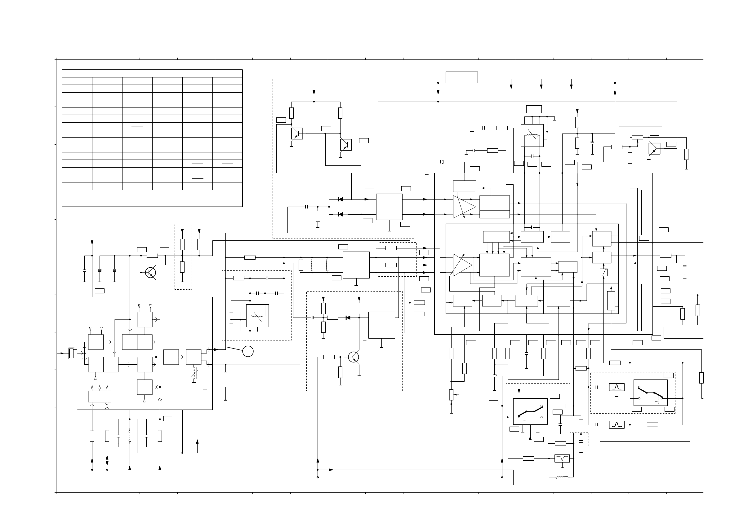
Platinenabbildungen und Schaltpläne / Layout of PCBs and Circuit Diagrams TVR 3710 …, TVR 5100 …, TVR 5500 … Platinenabbildungen und Schaltpläne / Layout of PCBs and Circuit Diagrams TVR 3710 …, TVR 5100 …, TVR 5500 …
Signal-Chassis – Empfangseinheit 2 / Frontend 2 (TU2)
4561 7 8 9 101112131415161723
VERSION
A
B
Pos.
1301
1320
1340
1345
1346
3322
3339
C
5307
7300
for TDA 9800 only:
D
for TDA 9812 only:
E
F
2306, 3319, 3331, 3345, 4033, 4035, 4036, 4038, 4041, 4043, 4301, 4302, 4304
2300, 2307, 2317, 2320, 2325, 3318, 3323, 3328, 3332, 3346, 4031, 4034, 4037, 4040, 4042, 4303
+12A
2333
100n
GNDT
VCC2
G
I
BPF
RF
TUNERCABLE
H
BPF
1501
I
PLL
CL
J
3304
100E
K
SCL2
*
PAL-BG PAL-I PAL-BG/SEC-L PAL-BG/SEC-DK
UV916S/PH
G1966M
4k7 22k 4k7
270E 100E 120E
U944C
G1965M
TRAP 6,0MHz
BP 6,0MHz
4k7
270E
UV916S/PH
G1965M
TRAP 5,5/6,0MHzTRAP 5,5MHz
BP 5,5MHzBP 5,5MHz
BP 6,0MHz
0E4039
0E 0E4044
15uH 5u615uH
TDA9800T
TDA9800T
TDA9812T7301
+12A
5TS2
8k2
3301
2301
12V
16V
10u
16V
2311
47u
GNDT
for MSTD only
delete for MSTD
56
AGC
2V 2V
3300
1k
7304
BC848B
IIIUI
27k
3302
GNDTGNDT
1301
3303
for PAL-I only
*
VCO
III
MIX
AGC
AMP
CS
5TS2
4561 7 8 9 101112131415161723
AGC
IIIUI
DA
3305
from CO
U
2302
100E
SDA2
to/from CO
VCC1
100n
5300
5TS
6u8
MIX
VCO
2303
GNDTGNDT
BPF
111213 14 15
16V
50V
22k
3306
100n
+33V
6k8
delete
for PAL-I
IF
UV916S/PH
G1966M
TRAP 5,5/6,5MHz
BP 5,5MHz
BP 6,5MHz
5u6
TDA9800T
3347
100E
2329
not used
GNDT
17
16
GNDT
MT
GNDT
4032
0E
delete for MSTD
2332
2330
not used
6
5302
1
2
40,4MHz-TRAP
1
5TS2
4k7
3313
0V
DTC124EK
7306
GNDT
2304
1n
3312
GNDT
EL0405
3307
5301
1u
not used
220p
2328
120p
2331
41859
34
1n
for MSTD only
MNT2
for MSTD only
4k7
3315
2,5V
DTC124EK
7307
GNDT
6300
BA582
6301
4k7
BA582
0V
1
1320
EL0606
5305
delete for MSTD
5TS2 5TS2
3349
3350
GNDT
2
for MSTD only
1u
0V
3k3
3343
6302
4k7
BA582
3k3
3344
3k3
3k3
3351
GNDT
H = B/G
L = D/K or MSTD
from CO
3
GNDT
3342
GNDT
for SEC-DK only
65mV
2,5V
*
1k
1
2
GNDT
7313
BF570
0V
1
2
4
5
1324
L9360M
1322
L9453M
3
GNDT
4020
0E
delete for MSTD
4030
0E
4
5
3
GNDT
3,2V
4
5
3,2V
3346
680E
3345
680E
GNDT
3,3V
3,3V
1,8V
*
*
SB1_2
2u2
28
27
1
2
12
16
H = SEC L'
L = PAL, SEC L
from CO
*
2300
50V
SIF AMP.
TDA9800T/V3
7300
1
VIF AMP
2
TUNER
*
0E
4043
22k
3341
GNDT
from TV from TVfrom AL
+12A5TS +33V
AFC2
42518
5303
2308
2,8V 2,8V
VCOWAVE
VIDEO
DEMODULATOR
AGC
DETECTOR
*
100n
2325
GNDT
7312
HEF4053
Vee
E
61678
-7V
4041
0E
123
46
8p2
2122 20
1617
8p2
BUFFER AND
7
4,9V
*
0E
4039
for MSTD only
Y0
12
Y1
13
Vss
GNDTGNDT
-6V
GNDT
NOISE
CLIPPING
14
1,9V
1,9V
*
3318
*
2307
180E
220n
GNDT
*
3319
*
2306
390E
100n
GNDT
2,5V
65
SIF AGC
INTERCARRIER
MIXER
AM DEMODULATOR
*
TRAVELING
DIVIDER
FREQUENCY
DETECTOR
AND PHASE
DETECTOR
IF
AGC
34 58
43
1V 3V 0,15V
AGC
*
0E
4300
2,5V
19
25
*
0E
4040
*
0E
4042
AGC2
2324
GNDT
4,9V
50V
2u2
11
14
1,9V
5TS1
Vdd
S
Z
H = PAL
L = SECAM
delete for MSTD
PSS2
from CO
5TS1
18k
3320
18k
3321
GNDT GNDT
2,8V
9
3,6V
2309
100n
TDA9812T
156
AFC
VIDEO
AMPLIFIER
13
19
18 26
2V 2V 2V
3348
330E
2315
220p
3340
680E
*
1340
13
2
GNDT
*
5307
4038
0E
*
3339
2327
GNDT
*
4037
*
100p
AMPLIFIER
FM-PLL
11
17
0E
2313
47p
2314
47p
4303
7301
AF
IRV
20
4036
0E
1346
3
2
GNDT
for SEC-DK
or MSTD only
1345
3
2
GNDT
AFC2
to DE
TDA9800: PHASE
TDA9812: L'-ADJ2
3322
*
3,6V
*
0E
*
0E
4302
GNDT
14
65mV
DTC124EK
7308
for MSTD only
*
*
2V
7312
HEF4053
4044
delete
0E
10
13
11
12
8
23
24
4,8V
E
2,4V
2,3V
*
3323
5k6
2,1V
2,4V
0V
4,9V
S
Z
*
*
GNDT
*
4034
GNDT
10
9
10
7
18
15
2,7V
*
*
1
Y0
2
Y1
115
2,7V 2,7V
*
1
for MSTD or SEC-DK
4304
GNDT
2317
0E
0E
10n
*
4033
GNDT
*
4035
*
0E
0E
4 - 55 GRUNDIG Service
4 - 56 GRUNDIG Service
Page 70
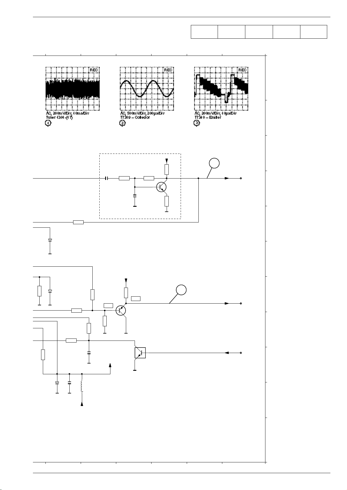
TVR 3710 …, TVR 5100 …, TVR 5500 … Platinenabbildungen und Schaltpläne / Layout of PCBs and Circuit Diagrams
4033
GNDT
*
4035
Reference
AL ..............P 4-65
BUPI ..........P 4-68
CO .............P 4-43
DE..............P 4-49
IO...............P 4-59
OHA...........P 4-69
PLSP .........P4-19
PSSP2.......P 4-37
TU2............P 4-55
T
ube PCB
...P 4-33
TV..............P 4-51
TXT............P 4-58
VS..............P 4-61
18 19 20 21 22 23
1301 G 4
1320 F 8
1322 D 9
1324 G 9
1340 K14
1345 J15
A
1346 I15
1501 I 1
2300 C11
2301 F 1
2302 J 2
2303 J 3
2304 D 7
2306 C11
2307 B12
2308 C13
2309 B14
2311 F 2
B
2313 I15
2314 J15
2315 J14
2316 E18
2317 F17
2318 D19
2319 D20
2320 G18
2321 J18
2322 J18
delete for MSTD
+12A
2
2k2
DTC124EK
7311
3326
7309
BC848B
1k
3327
GNDT
AFV2
to IO
3
VFV2
to IO
MTA
from DE
1,1V
1k
5TS1
3324
4k7
5TS1
3329
GNDT
270E
7310
BC858B
2318
220n
*
4031
0E
16V
2316
22u
GNDT
*
50V
0E
2320
2u2
GNDT
3332
5k6
0E
16V
2322
2321
22u
GNDT
GNDT
3331
1k
*
100n
5TS
*
5304
*
*
4301
2323
GNDT
6u8
3328
0E
1k
3330
GNDT
100n
2319
GNDT
1,8V
GNDT
10n
3325
680k
C
D
E
F
G
H
I
J
K
2323 I19
2324 I12
2325 H13
2327 J14
2328 F 6
2329 G 5
2330 F 6
2331 G 7
2332 F 6
2333 F 1
3300 E 3
3301 E 4
3302 F 4
3303 E 4
3304 J 1
3305 J 2
3306 J 3
3307 F 7
3312 D 7
3313 B 6
3315 B 8
3318 B12
3319 C12
3320 B14
3321 B14
3322 B16
3323 E16
3324 D20
3325 D20
3326 C21
3327 D21
3328 G19
3329 G20
3330 H19
3331 G18
3332 H18
3339 J14
3340 J14
3341 I11
3342 G 8
3343 G 8
3344 H 8
3345 G10
3346 G10
3347 F 5
3348 I14
3349 G 7
3350 G 7
3351 I 8
4020 E 9
4030 F 9
4031 E18
4032 E 5
4033 G17
4034 G17
4035 I17
4036 H15
4037 H14
4038 H14
4039 H13
4040 H12
4041 K13
4042 H11
4043 H11
4044 J16
4300 H12
4301 H19
4302 C15
4303 B15
4304 C17
5300 J 2
5301 F 7
5302 G 5
5303 C13
5304 J18
5305 F 7
5307 K14
6300 D 8
6301 D 8
6302 G 8
7300 E11
7301 D15
7304 F 3
7306 B 7
7307 C 8
7308 C16
7309 D21
7310 G20
7311 I20
7312 I13
7312 I16
7313 H 8
18 19 20 21 22 23
GRUNDIG Service 4 - 57
Page 71
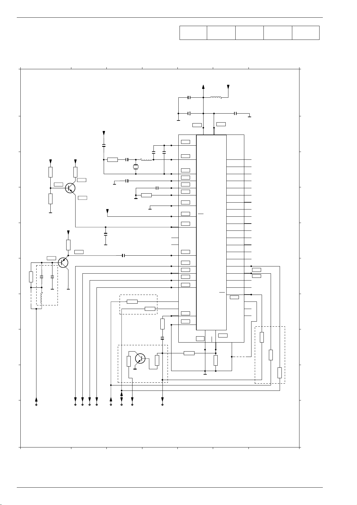
Platinenabbildungen und Schaltpläne / Layout of PCBs and Circuit Diagrams TVR 3710 …, TVR 5100 …, TVR 5500 …
Signal-Chassis – Teletext "DOS" (TXT)
A
B
C
D
E
F
G
H
I
IC7880: Only for 1 Frontend (Tuner) Version
IC7881: Only for 2 Frontend (Tuner) Version
5DDA
5DDA 5DDA
10k
3799
9118
3882
2,2V
5k6
3883
GNDTXT
1,6V
0E
2894
2893
GNDTXT
5882
not used
5DDA
1k
3889
7883
BC858B
GNDTXT
100E
3890
7882
BC848B
2,2V
4,9V
1,9V
100n
2886
3880
3k3
5DDA
100n
2889
GNDTXT
GNDTXT
2890
100n
2885
1n
1800
2887
100n
GNDTXT
3884
100E
for SAA5281 only
3897
GNDTXT
5881
4u7
27MHz
3881
27k
GNDTXT
3885
100E
7884
not used
2884
2888
100n
3896
4561 723
10p
2883
1k
3886
100n
2891
Reference
AL ..............P 4-65
BUPI ..........P 4-68
47u
GNDTXT
2,1V
2
15p
3,6V
3
4
4,9V
6
2,1V
7
2,5V
9
0V
11
4,9V
13
1,9V
18
21
ODD
22
Y
2,2V
8
0V
19
15
16
17
23
SCL
24
SDA
2,2V
12
5
SAA5281
7880
for SAA5281 only
CO .............P 4-43
DE..............P 4-49
IO...............P 4-59
2880
100n
2881
5880
10u
16V
4,9V
110
1
VDD1
VDD2
2
OSCOUT
3
OSCIN
0V
4
OSCGND
6
REF+
7
BLACK
9
IREF
11
POL
13
VCR/FFB
18
RGBREF
8
CVBS
19
BLANK
0V
15 24
R
0V
16
G
0V
17
B
7881
SAA5254
12
STTV/LFB
0V
5
VSS1
VSS2
VSS3
14 20
0V
14 25
4085
0E
20
4088
GNDTXT
from TV
5DS5DDA
2882
100n
4,9V
40
ic1
39
ic2
38
ic3
37
ic4
36
ic5
35
ic6
34
ic7
33
ic8
32
ic9
31
ic10
30
ic11
29
ic12
28
ic13
27
ic14
26
ic15
25
SDA
SCL
23
Y
22
ODD
21
COR
0V
VSS3
COR
0E
for SAA5254 only
OHA...........P 4-69
PLSP .........P4-19
PSSP2.......P 4-37
GNDTXT
48
47
46
45
44
LINE23
43
42
41
40
39
38
37
CLK-O/P
36
CLK-EN
35
34
33
ic13
32
ic14
31
ic15
30
ic16
29
ic17
0V
28
ic18
27
ic19
26
ic20
9215
for SAA5254 only
TU2............P 4-55
T
ube PCB
TV..............P 4-51
5V
5V
0E
4086
3887
for SAA5254 only
100E
...P 4-33
100E
3888
TXT............P 4-58
VS..............P 4-61
1800 C 3
2880 A 5
2881 A 5
2882 A 6
2883 C 4
2884 C 4
2885 C 3
A
2886 B 2
2887 C 3
2888 C 4
2889 E 2
2890 E 3
2891 H 4
2893 F 1
2894 F 1
3799 F 1
3880 C 3
3881 D 4
B
3882 C 1
3883 D 1
3884 G 3
3885 G 4
3886 G 4
3887 H 7
3888 I 7
3889 E 1
3890 C 2
3896 H 4
C
3897 H 3
4085 H 5
4086 H 7
4088 H 5
5880 A 6
5881 C 4
5882 G 1
7880 H 5
7881 G 5
7882 D 2
D
7883 F 1
7884 H 4
9118 G 1
9215 H 6
E
F
G
H
I
VTV
J
from IO-Part
GTXT
RTXT
BLTXT
to TV-Part
BTXT
SCL
SDA
from CO-Part
to/from CO-Part
BRI
to TV,TXT-Part
STTV
to TV-Part
J
4561 723
4 - 58 GRUNDIG Service
Page 72
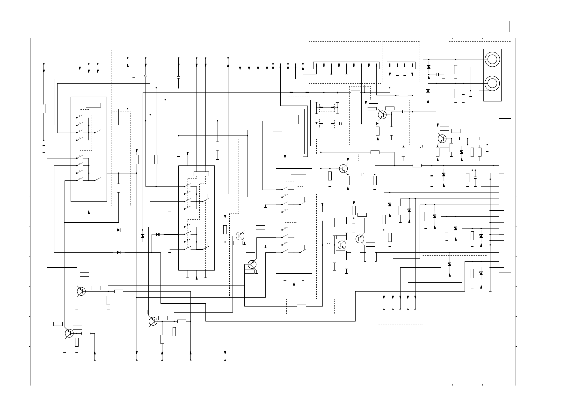
TVR 3710 …, TVR 5100 …, TVR 5500 … Platinenabbildungen und Schaltpläne / Layout of PCBs and Circuit Diagrams
Reference
AL ..............P 4-65
BUPI ..........P 4-68
CO .............P 4-43
DE..............P 4-49
IO...............P 4-59
OHA...........P 4-69
PLSP .........P4-19
PSSP2.......P 4-37
TU2............P 4-55
T
ube PCB
...P 4-33
TV..............P 4-51
TXT............P 4-58
VS..............P 4-61
Signal-Chassis – IN/OUT (IO)
TVR 3710 …, TVR 5100 …, TVR 5500 … Platinenabbildungen und Schaltpläne / Layout of PCBs and Circuit Diagrams
for View Select
A
from AL
AMLP
only
B
3525
390E
C
ASC
ACI
22n
2507
D
GNDTV
TU1
VSC
VCI
E
F
G
H
I
-0,8V
J
7506
BF824
5AS
10
VDD
TU1
1
5
2
4
PB
12
14
15
11
PB
HEF4052BT
7591
VSS
VEE
8
7
-7V
1,4V
for View Select
only
7507
BF824
GNDTV GNDTV
1V
3521
1k5
1k5
3522
GNDVS
GNDVS
451 6 7 8 9 10 11 12 13 14 15 1623
from TU2
+12A
3526
10k
AFV2
2511
25V
4u7
from DE
VS1
LOGIC
916
from DE
VS2
ATV
to TV
GNDTV
3
4051
0E
delete for View Select
13
0E
4052
6
GNDTVGNDTV
6515
1N4148
6514
1N4148
6513
1N4148
3524
3523
1k
1k
2,4V
BF824
7503
GNDTV
0,5V
2Vpp 1Vpp2Vpp1Vpp
only
for Tuner 2
0E
4053
delete for Tuner 2
TU1/2
ASC
ACI
PB
GNDTV
TU1/2
6512
VSC
1N4148
VCI
PB
GNDTV
1,7V
3520
220E
for TU2 only
2508
3542
GNDTV
1
5
2
4
12
14
15
11
3519
220E
delete
for TU2
GNDTV
AFV1
3518
220E
from TV
RS1
25V
4u7
100k
5AS
10
VDD
LOGIC
HEF4052BT
7592
VSS
VEE
8
7
-7V
from DE
RS2
916
6
GNDTVGNDTV
from DE
3527
GNDTV
3
13
100k
only
for Tuner 2
+12A
10k
3517
AMLR
to AL
for Tuner 2
only
1,7V
from TV
from AL
+12A -7V5AS
7501
BF824
GNDTV
-1,6V
0,5V
from TV
from VS
from DE
from DE
OS2
OS1
5SE2
4054
0E
delete for SCART Output Select
for SCART Output Select only
5AS
VDD
TU2
1
5
TU1
2
4
GNDTV
TV
12
TU2
0V
14
TU1
15
11
GNDTV
TV
7502
BF824
GNDTV
HEF4052BT
7593
VSS
8
from DE
ISON
8
10
VEE
7
-7V
from DE
MTA
AKP
1502
LOGIC
916
6
GNDTVGNDTV
4055
0E
AKM
to CO
24
1972
GNDTV
3541
3
13
AKM
9
100k
10
+12A
3515
9
delete for SCART Output S.
for VCD only
VCCD
-7V
8
7
-7V
3536
AKP
25
1502
GNDTV
AKP
26
1502
2u2
100k
3503
10k
39k
3531
2510
10u
16V
12k
3532
GNDTV
VCI
6
GNDTV
6k8
delete for
2513
50V
11,2V
2,1V
front A/V
3539
-7V
3514
3516
GNDTV
ACCDM
MTA
GNDTV
4
5
4501
0E
5SE2
or Plug Print
delete for VCD
5AS
7509
BC848B
2501
10u
16V
3k3
+12A
22E
3530
12V
2506
100n
470E
GNDTV
7500
BC848B
3513
1k2
820E
3
BC848B
not used
7508
BF824
3,4V
3533
150E
3534
150E
ISON
2
4,8V
3545
220E
7505
4502
0E
4500
3501
GNDTV
0E
ACIM1
3537
100k
1
-1,1V
3k3
-7V
3511
for Plug Print only
to BUPI
GND
GND
3
4503
0E
2512
220n
3540
GNDTV
75E
ACIM
4
100k
6509
-7V
1918
1
-0,4V
3538
GNDTV
6510
-7V
6k8
VCI
2
GNDTV GNDTV
100k
BZX79-C27
3510
GNDTV
for
RGB-SCART
4k7
3512
only
GNDTV
to TV
to TV
GREEN
RED
to TV
8SC
to CO
BLUE
for VCD only
Pos.4503
2514
2u2
50V
3500
470E
BZX79-C12
3509
GNDTV
BLSC
to TV
6516
-7V
6517
-7V
BC848B
75E
100n
BZX79-C12
2509
BZX79-C12
5AS
7504
3535
-7V
2503
470p
GNDTVGNDTV
6508
-7V
GNDTV
4,9V
-1,1V
2k2
GNDTV
6503
BZX79-C12
-7V
BZX79-C12
75E
3508
GNDTV
6507
-7V
75E
3528
GNDTV
3529
100k
2515
GNDTV
GNDTV
for front A/V only
-0,5V
2502
220n
100k
3502
6500
-7V
GNDTV
6506
BZX79-C12
-7V
BZX79-C12
1n
GNDTV
3504
6k8
6k8
3505
BZX79-C12
47k
3543
2505
GNDTV
75E
3506
GNDTV
75E
3507
GNDTV
VID
GNDV
AUD
GNDA
47k
3544
GNDTV
470p
6504
-7V
6505
-7V
AV CINCH
1919
1
2
2504
470p
GNDTV
3
4
5
6
Swtching
8
blanking
16
blue
7
9
11
13
red/c
15
17
14
BZX79-C12
18
VideoOut
19
10
20
21
1915
BZX79-C12
GNDTV
VIDEO
AUDIO
AudOutR
AudInR
AudOutL
AudInL
green
VideoIn
1502 B 9
1502 C10
1502 C10
1915 H16
1918 A12
1919 B16
A
1972 A10
2501 E11
2502 D15
2503 E14
2504 D16
2505 E15
2506 F11
2507 D 1
2508 B 5
2509 A14
2510 G10
2511 A 4
B
2512 C13
2513 C11
2514 D13
2515 B15
3500 D13
3501 E12
3502 D15
3503 E10
3504 C15
3505 D15
C
3506 G15
3507 H15
3508 G14
3509 F14
3510 F13
3511 F12
3512 G12
3513 G11
3514 G11
3515 F10
D
3516 H11
3517 G 7
3518 J 5
3519 J 5
3520 J 5
3521 J 2
3522 J 2
3523 I 3
3524 I 3
3525 C 1
E
3526 D 4
3527 D 7
3528 A15
3529 B15
3530 F11
3531 G10
3532 H10
3533 G12
3534 H12
3535 D14
F
3536 B11
3537 C12
3538 C12
3539 E11
3540 D13
3541 C10
3542 D 5
3543 E15
3544 D15
3545 B12
G
4051 C 4
4052 E 3
4053 D 5
4054 C 9
4055 I 9
4500 D12
4501 B11
4502 C12
4503 B13
6500 D15
H
6503 E14
6504 G15
6505 H15
6506 G15
6507 H14
6508 F14
6509 F13
6510 F12
6512 G 5
6513 G 3
I
6514 G 4
6515 G 3
6516 A14
6517 B14
7500 G11
7501 G 8
7502 H 8
7503 J 4
7504 D14
7505 C12
J
7506 J 2
7507 I 2
7508 G12
7509 E11
7591 E 2
7592 H 5
7593 H 9
K
VP
from VS
VTV
to TV,TXT
VFV2
from TU2
VFV1
from TV
VR
to VS
451 6 7 8 9 10 11 12 13 14 15 1623
GRUNDIG Service 4 - 59
K
GRUNDIG Service 4 - 60
Page 73
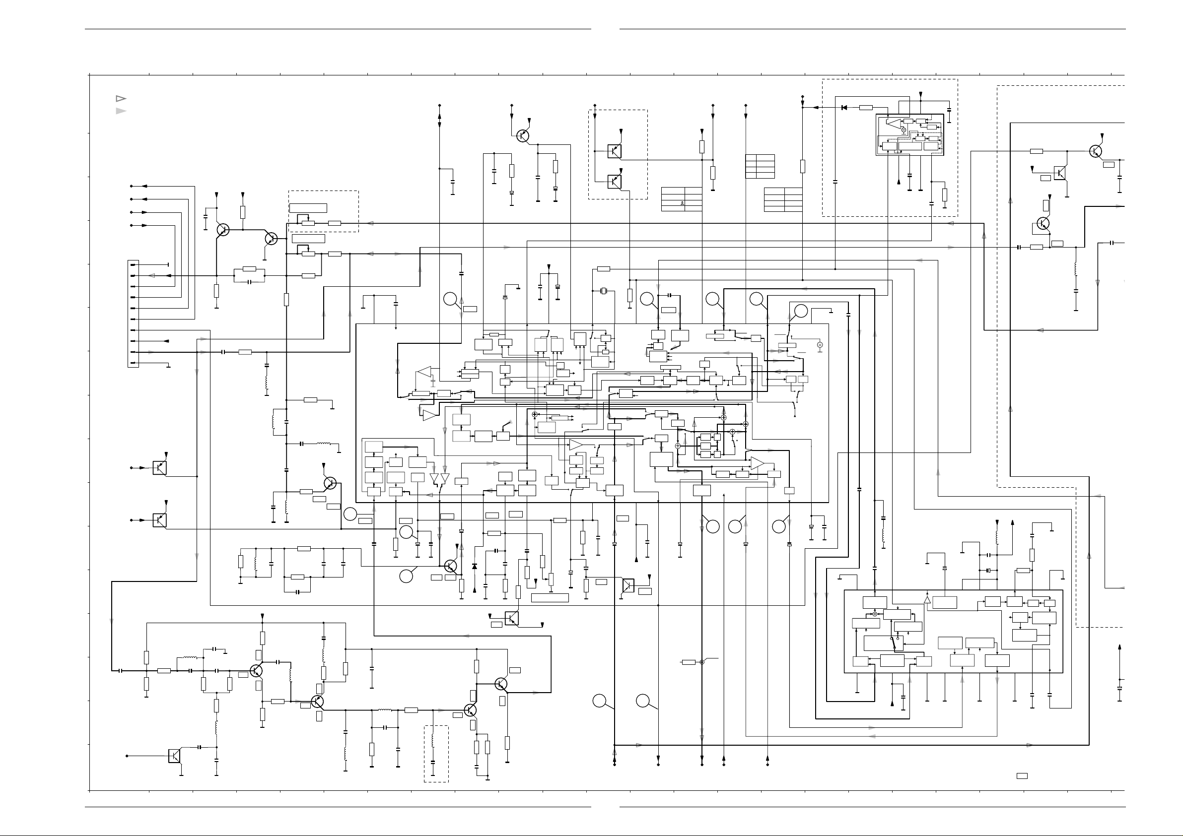
Platinenabbildungen und Schaltpläne / Layout of PCBs and Circuit Diagrams TVR 3710 …, TVR 5100 …, TVR 5500 … Platinenabbildungen und Schaltpläne / Layout of PCBs and Circuit Diagrams TVR 3710 …, TVR 5100 …, TVR 5500 …
B
S
V
16V
47u
Signal-Chassis – Video/Chroma (VS)
4561 7 8 9 10 11 12 13 14 15 16 17 182 19 20 21 22 233
A
B
C
D
E
F
G
H
I
J
K
L
M
N
O
P
Record
Playback
ENVC
TRIV
HSC
HP1
to/from DE
1902
1
GNDVS
2
FMRV
3
HP1
4
HSC
5
TRIV
6
ENVC
7
CSYNC
8
5VAS
9
FMPV
To OHA 1910
GNDVS
from DE
from DE
2043
1n
FMSW
from DE
IREC
10
4,8V
4,8V
DO
GNDVS
3031
3032
18k
18k
5SE
5SE
3033
330E
0V
7009
DTC124EK
GNDVS
5AS
PLAY
GNDVS
PLAY
4,9V
7015
DTA124EK
1,9V
5,2V
7016
DTA124EK
3,4V
5008
8u2
2044
47p
0V
GNDVS GNDVS
2047
56p
2042
GNDVS
REC
1k
3034
100n
3025
GNDVS
2045
47p
2046
27p
3035
2048
5006
4,8V
BC848B
1V
1k
2040
10n
470E
15u
82p
7019
GNDVS
270E
3036
68p for LP
5SE5SE
4k7
3026
7018
1,7V
BFS19
GNDVS
3024
1k5
2041
22p
3022
1k2
2039
5012
220u
GNDVS
GNDVS GNDVS
1k
3019
5003
100u
2034
5PB
680E
3037
7020
0.6V
BFS19
2.2V
0.3V
0V
1.4V 3.0V
560E
3038
GNDVS
FM PROCESSING
4561 7 8 9 10 11 12 13 14 15 16 17 182 19 20 21 22 233
5010
2035
56p
2049
68p
3039
390E
0,7V
15u
10p
3023
2037
2036
68p
5009
for MSTD only
SECAM-CURR.
10k
3027
PAL-CURR.
10k
3029
3048
not used
2k7
REC
3021
1k
18p
Y-REC-BPF
2038
5011
100u
220p
5SE
4,8V
180p
3020
2,7V
470E
2V
27u
3017
4k7
2%2%
3018
1k3
2%2%
2033
68p
2%2%
27u
5007
1.5V
0V
2032
2050
5005
3040
0.6V
0V
PLAY
GNDVS
7010
BC848B
2,7V
200p
68p
15u
330E
2.2V
7021
BF824
1.2V
3028
3030
3,4V
4k7
2k7
GNDVS
2%2%
CKPAL
from/to DE
GNDVS
2001
from DE
ITRICK
5SE
from DE
INTSC
for NTSCPB only
5,2V
1k
3000
2004
GNDVS
7000
BC858B
2V
8k2
3001
47n
2008
50V
1u
50V
2009
1u
GNDVSGNDVS
4,8V
5SE
5V
7002
DTA124EK
5V
7003
DTA124EK
0,2V
0V
Color Vector
Normal
LP features
NTSC-PB H (5V)
Pin 27
L (0V)
Z
4,8V
22n
47n
2003
GNDVS
5SE5SE
3051
(1.2…3V)
from DE
HSC2
not used
22k
3004
GNDVS
LPV
LP Z (2.5V)
S-LPSPH (5V)
REC
REC
5SE
10n
2002
GNDVS
50V
2005
100n
2000
GNDVS
GND VCC GND
7051
LA7437A
DEMOD
DOUBLE
LIM
3,2V
64
2,3V
1,4V
40
41
42
SUB
LPF
FM
FM
AGC
1
ACC-DET
DET
CARRIER
SHIFT
FM
MOD
YNR-CTL
(TO AVNS)
COM
R
KILLER
P
6dB
DO
MAIN
DO
DEEMPH
4.2V
REF
P
3
2
4,2V3,4V
2,7V
62
16V
2k2
65
2029
GNDVS
2028
10u
GNDVS
3.2V
2031
1n
2030
3016
10p
GNDVS
10n
C-LPF
39
R
4
3,2V
2,3V
4,8V
7007
BC848B
1.6V2.3V
BGP2
BGP1
5SE
NL
DEEMPH
WHI
NOI CAN
CLAMP
2027
3015
GNDVS
KIL-DET
R
P
2.6V
2k2
2,2V
38
ID-DET
5
3,2V
16V
10u
3,1V
PICTURE
CONTROL
6000
5PB
321FH
VCO
1N4148
GNDVS
PLAY
1k5
1.2V
0V
for SECAM only
3044
0.6V
0V
3045
2056
7014
BFS19
680E
GNDVS
3041
2051
5004
GNDVS
1k2
100u
2052
GNDVS
560p
330p for SECAM
3042
560E
100n
5013
2053
27p
3043
1k
15u
5014
2055
560u
120p
33p
2054
GNDVSGNDVS
GNDVS
2,7V
37
CHROMA N.C.
2,2V
6
4,4V
3014
2k7
2%2%
2025
47p
180p
2062
5PB
0.8V
1k for MSTD
3.8V
0.5V
470E
3046
100p
2%2%
0V
SLD
90
P.S.
PAL
Y/C
MIX
W/D
CLIP
MAIN
EMPH
2026
3013
GNDVS
0V
3047
GNDVS
1u
2,7V
36
7
2,2V
390p
560E
0.6V
7013
BC848B
3.2V
2k2
4,4V
5V
2%
8k2
3062
4,9V
DTA124EK
7005
DETAIL
ENH
EMPH
2024
3012
35
NL
8
2,7V
18k
0,5V
18p
5SE
SYNC-FREQU.
0V
100n
2006
2007
GNDVS GNDVS
4,8V
34
P
R
REC
PB
AFC
APC
DET
DET
BGP2
x2
DELAY
CROT
4PHASE
SHIFTER
BGP.GEN
HALF H.
KILLER
FMAGC
DET
9
3007
not used
100k
3011
10k
3010
5SE
16V
47u
BGP2
CONV
P
2023
GNDVS
3002
1k8
1000
4,433619MHz
2,4V
2V
33
SW2
REC
VXO
APC
DET
3RDLOCK
PROTECT
SW1
2FSC
SUB
BGP1
BGP2
P
R
6dB
P
R
SYNC
LPF
SEP
DELAY
CLAMP
AGC
DET
R
113212
10
2,5V
1,6V
2021
3008
not used
16V
16V
2022
5V
22u
10u
0V
100k
3009
GNDVS GNDVS
60
6k8
3003
3,7V
GNDVS
31
PAL /
MESECAM /
NTSC
XO
P
FSC
BPF
R
1/2
VIDEO
AGC
VCC
3,2V 4,8V 0,4V 3,2V 1,9V 2V
2,9V
2010
10n
7063
0,15V
0,16V
2,4V
FSC
CHROMA
BPF
NAP
BP.AMP
B.DEEM
KILLER
CLAMP
CLAMP
QV/QH INS
CHARA INS
W/D CLIP
BALANCER
MAIN
CONV
BGP1
KIL
Y-LPF
N.C.
+
-
2FSC
NT*REC
P
R
SUB
BPF
P
R
1330142915
28
Y/C-MIX
1,8V
BURST
EMPH
DO
REC
2020
not used
16V
10u
7001
DTC124EK
5SE
100n
2019
5PB
0V
16V
2018
10u
GNDVSGNDVS
0,8V
3005
1k
71
VR
from IO
to DE
CSYNC
69 68
0V 2,4V
6dB AMP
B.G.
ACC
AMP
P
REC
LIM
K2
CORR
LIM
K1
VIDEO
4 PHASE SHIFTER
AMP
1627172618251924202321
60mV 2,4V
SLP/LP/SP
MESEC
MESEC
R
P
ACC
DET
Pin 41
R
PB
+
-
+
+
+
DO
P
R
CLAMP
LPF
2,1V
61 67
2017
PLAY
VIDEO
VP
CROT
to IO,CO
from DE
from DE
Pin 25
LPF
+
16V
10u
L (0V)
PAL
MESECAM
NTSC
FFP
Pin 30
L (0V)
Z (2.5V)
H (5V)
2,4V
MESEC
INVERT
REC NTSC
REC NTSC
PB ALL
B.G.
B
R
REC APC-DET
PB APC-DET
VCA
ATT
0V 1,1V
66
2016
from DE
MES
from CO
2k7
3071
for MSTD or SEC-DK only
68
0V
22
MESEC
B.G.
A
P
SW1
2,2V
50V
2015
1u
50V
GNDVS
GNDVS
1u
for SEC-DK only
1N4148
6070
MESECAM
DETECTOR
1n
2071
for MSTD only
GNDVS
2011
10n
2014
GNDVS
2,3V
VR
3072
1k
10
7070
LA7356
SW
LIMAMP
12345
10n
10n
2012
2013
15u
5001
GNDVS
10n
2060
0,16V1,4V
GND
SAMPLE
AND HOLD
OUTPUT AMP
CCD
CCD
2.5 STAGES
CENTER
GND
1
853 STAGES
CLOCK
SWITCHING
CIRCUIT
AUTO BIAS
CIRCUIT 1
23456789
4,8V
GNDVS
5SE2
COMP
FREQ.PHASE TIMING
CONVERTER
CHROMA-IN
5SE
330p
CLOCK
CCD
852 STAGES
VCC
2,3V
2069
GNDVS
5SE
for MSTD only
6789
100n
2073
VCC
LPF
PD2
2075
10n
CLOCK
PD1
GND
10n
GNDVSGNDVS
CENTER
GNDVS
2021222324
BIAS
1HDL
SLH
GEN
2076
BGP-IN
33k
3075
470p
GNDVS
2061
RD VOLTAGE
GEN
7060
LC89973M
AUTO BIAS
CIRCUIT 2
GNDVS
50V
1u
VCC GND
SYNC TIP
CLAMPBIAS
2,2V
0V7,9V
171819
CCD
848.5 STAGES
GND
47u
CLOCK
2064
10n
2065
4,8V4,8V
SHAPER
5SE
5015
16V
VCC
WAVE
SAMPLE
AND HOLD
OUTPUT AMP
3114
CSYNC
4k7
5PB
5,2V
0V
5PB
0,7V
7105
BC848B
3115
2117
1k
1n
REC
5SE2
GNDVS
10n
2066
22u
1k
3060
3061
82k
2V
2V
13141516
1/3 VCO
DETECTOR
2,4V1,2V 1,2V
2068
GNDVS
GND
TIMING
GENERATOR
10n
FSC
2067
PHASE
COMP
CLOCK
DRIVER
CLOCK
DUTY CYCLE
GND
10 11 12
GNDVSGNDVSGNDVSGNDVS
...V MEASURED IN PLAYBACK MODE
...V MEASURED IN RECORD MODE
3,2V
1,3V
5,2V
GNDVS
1n
7104
DTC124EK
GNDVS
0V
5106
2118
GNDVS
REC
330u
5SE1
5,2V
7103
BC848B
0V
0,3V
2115
GNDV
2116
10n
33p
2058
GND
5P
4 - 61 GRUNDIG Service 4 - 62 GRUNDIG Service
Page 74
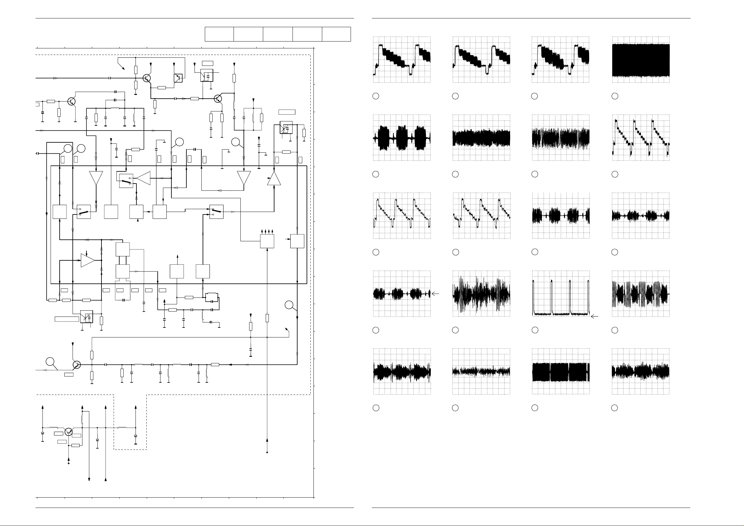
TVR 3710 …, TVR 5100 …, TVR 5500 … Platinenabbildungen und Schaltpläne / Layout of PCBs and Circuit Diagrams
AC, 200mV/Div, 10µs/Div
IC7051-(12)
REC
60
AC, 100mV/Div, 20µs/Div
IC7051-(38)
REC
63
AC, 100mV/Div, 20µs/Div
IC7051-(20)
66
PB
AC, 200mV/Div, 20µs/Div
2,5V
IC7051-(29)
70
PB
AC, 50mV/Div, 20µs/Div
IC7051-(29)
70
PB-SEC
AC, 200mV/Div, 20µs/Div
IC7151-(17)
73
REC
AC, 50mV/Div, 20µs/Div
IC7151-(23)
74
PB
2
TVR 3710 …, TVR 5100 …, TVR 5500 … Platinenabbildungen und Schaltpläne / Layout of PCBs and Circuit Diagrams
ANTICLOCHE
5100
42415
4.286MHz61
3
MT
NC
3101
3k3
0,1V
S
76
CSI
TU2............P 4-55
T
ube PCB
...P 4-33
TV..............P 4-51
3100
330E
GNDVSGNDVS
0,1V
88mV
COLOR
KILLER
1
0V
TXT............P 4-58
VS..............P 4-61
1000 E12
1902 D 1
2000 E 7
2001 C 8
2002 E 9
2003 B 9
A
2004 C10
2005 E10
2006 E10
2007 E11
2008 C10
2009 C11
2010 E13
2011 F17
2012 J18
B
2013 J18
2014 K17
2015 K17
2016 K16
2017 K15
2018 K14
2019 K13
2020 K12
2021 K12
C
2022 K11
2023 L11
2024 K10
2025 K 9
2026 K10
2027 K 9
2028 K 8
2029 K 8
D
2030 K 7
2031 K 6
2032 K 5
2033 L 5
2034 K 4
2035 J 4
2036 I 5
2037 H 5
2038 I 5
E
2039 G 4
2040 F 3
2041 E 4
2042 C 3
2043 N 1
2044 N 2
2045 M 3
2046 N 3
F
2047 P 3
2048 P 3
2049 N 4
2050 M 5
2051 O 6
2052 N 7
2053 O 7
2054 P 7
G
2055 P 8
2056 P 9
2058 N24
2059 N26
2060 K18
2061 K20
2062 L 9
2064 K21
2065 K21
H
2066 K22
2067 N22
2068 N22
2069 N19
2071 C17
2073 A20
2075 B19
2076 C19
I
2100 D32
2101 C31
2102 C31
2103 C30
2104 D29
2105 D28
2106 B29
2107 C27
2108 C27
J
2109 B26
2110 B26
2111 C26
2112 C25
2113 D26
2114 A26
2115 C24
2116 D24
K
2117 D21
2118 E23
2119 K31
2121 L26
2122 I27
2123 I27
2124 J28
2125 L27
2126 L28
L
2127 L28
2128 L29
2129 J29
2130 J29
2132 I30
2133 J30
2134 J30
2135 L29
M
2136 N27
3000 B10
3001 B11
3002 E12
3003 E12
3004 B14
3005 N14
3007 J11
N
3008 K11
3009 L11
3010 L11
3011 K10
3012 L10
3013 L10
3014 K 9
3015 L 9
3016 K 7
O
3017 K 5
3018 L 5
3019 K 4
3020 J 5
3021 H 5
3022 F 4
3023 E 5
3024 E 4
3025 E 3
3026 C 4
P
3027 D 5
3028 C 6
3029 D 5
3030 D 6
3031 N 1
3032 N 1
3033 N 2
3034 N 3
3035 O 3
3036 N 3
3037 M 4
3038 O 4
3039 N 4
3040 N 5
3041 N 6
3042 P 7
3043 O 7
3044 N 9
3045 P 9
3046 P 9
3047 O10
3048 E 5
3050 O25
3051 B14
3060 K22
3061 K21
3062 L10
3071 B16
3072 A18
3075 C20
3100 C33
3101 D33
3102 C32
3103 A31
3104 C30
3105 C30
3106 B29
3107 B28
3108 A27
3109 B27
3110 D27
3111 C26
3112 C24
3113 B24
3114 B22
3115 D22
3116 J31
3117 B28
3118 K25
3119 L25
3121 L27
3122 L30
3123 I24
3124 I25
3125 J26
3126 J28
3127 I29
3128 J32
3129 I25
5000 N25
5001 K18
5002 N24
5003 K 4
5004 P 6
5005 M 5
5006 O 3
5007 N 5
5008 M 2
5009 J 5
5010 H 4
5011 I 5
5012 G 4
5013 O 7
5014 O 8
5015 K21
5100 C33
5101 C31
5102 B31
5103 A29
5104 C27
5105 B26
5106 E23
5107 J30
5108 J25
5110 L28
5111 L29
5112 L27
5113 I30
5114 L30
5115 N27
6000 K 9
6070 A17
7000 B10
7001 L13
7002 B12
7003 C12
7005 M10
7006 N25
7007 K 8
7009 P 2
7010 I 6
7013 N10
7014 O 9
7015 I 2
7016 J 2
7018 C 4
7019 D 3
7020 N 4
7021 O 6
7051 H 6
7060 M20
7070 A18
7100 B30
7101 A28
7102 B25
7103 B23
7104 B23
7105 D22
7106 K25
7107 A28
7151 G28
AC, 500mV/Div, 10µs/Div
IC7051-(16)
61
AC, 100mV/Div, 20µs/Div
IC7051-(38)
63
AC, 100mV/Div, 20µs/Div
IC7051-(18)
67
REC
PB
PB
AC, 500mV/Div, 10µs/Div
IC7051-(16)
61
AC, 100mV/Div, 20µs/Div
IC7051-(1)
64
AC, 200mV/Div, 20µs/Div
IC7051-(24)
68
DC, 500mV/Div, 20µs/Div
IC7051-(14)
71
AC, 200mV/Div, 20µs/Div
IC7151-(18)
75
PB
PB
REC
REC
PB
AC, 200mV/Div, 2µs/Div
IC7051-(2)
62
AC, 100mV/Div, 20µs/Div
IC7051-(4)
65
AC, 200mV/Div, 20µs/Div
IC7051-(26)
69
0V
AC, 50mV/Div, 50µs/Div
IC7151-(29)
72
AC, 200mV/Div, 20µs/Div
IC7151-(1)
76
REC
PB
PB
REC
PB
Reference
AL ..............P 4-65
BUPI ..........P 4-68
CO .............P 4-43
DE..............P 4-49
IO...............P 4-59
OHA...........P 4-69
PLSP .........P4-19
PSSP2.......P 4-37
32 3324 25 26 27 28 29 30 31
5SE1
47k
5,2V
3108
CSI
2114
22n
03
48B
3113
V
560E
V
3112
2115
220p
GNDVS GNDVS GNDVS
116
10n
17 20 23 27 30 31
LIMITER/
BLANKING
0V
0V
7102
BC848B
1k
73
2,5V
0V
18
2,5V
1,2V
P
R
75
2112
10n
3111
GNDVS
2,5V
10dB
2110
100n
2109
15p
5105
150u
68p
2k2
2111
GNDVS GNDVS GNDVS
5SE1
2113
GNDVS
5,2V
POWER
2,5V
1,8V
47k
3109
GNDVS
10n
1,8V
150p
P
R
5104
3110
1k2
0V
DIVIDER
150u
2107
6dB
2108
100n
2119 2422
by 4
7101
BC848B
GNDVS
1k
3107
2105
0V
LIMITER
DTA124EK
3117
470E
PLAY
GNDVS
10n
2,7V
5SE1
7107
2106
10n
3,2V
VREF 5SE1
CLOCHE
42415
4.286MHz61
3
5103
3106
820E
74 72
2104
10n
3,3V
2,7V
1,2V
1,3V
25 32
NC
MT
GNDVS
4,0V
2,5V
7100
BC848B
1,8V
1k
3104
3105
390E
1n
2103
GNDVS GNDVS
1,8V
26 28
R
P
GNDVS
3103
2102
5102
680E
56u
VREF
22p
15u
2101
100p
3102
820E
5101
VREF
10n
2100
GNDVS
CK
88mV
10dB
2,5V
29
15dB
RS
P
5SE1
1k
3116
2119
GNDVS
10n
RSRS
SWITCH
INTERFACE
1,2V
2k2
3128
CSI
32 3324 25 26 27 28 29 30 31
from CO
5PB
2058
GNDVS
3123
10k
70
5002
6u8
16V
47u
0,8V
15
2,5V
2,5V
2,3V
3124
1k5
LF CL/ANTICLOCHE
5SE1
7106
5,2V
BC848B
2,6V
0,15V
7006
5V
5V
BC558B
5V
4,2V
5,1V
3050
4k7
IPBV
from DE
P
2,6V
2,5V
3129
18k
5108
42414
1.0715MHz
13
2k2
3125
4MT
NC
GNDVSGNDVS
4k7
3118
22u
to IO
5SE
33k
3119
GNDVS
2059
GNDVS
2121
1n
5AS
6,3V
220u
5AS
from TV
0,6V
5SE
5000
AGC
DETECTOR
1,1MHz
RECTIFIER
f
111416
1213 10 39
1,8V
3,7V
1,5V
2125
GNDVS
5SE1
GNDVS
2136
2,9V
3,8V
2123
100n
GNDVS
2126
5112
82u
22p
10p
16V
47u
1,5V
2122
10n
1k8
3121
GNDVS GNDVS
5115
15u
TDA4722/V2
7151
VOLTAGE
REFERENCE
2,5V
2,9V
3,8V 2,5V
VREF
3126
1k
2124
100n
2129
GNDVS GNDVS
5111
82u
8u2
2127
180p
5110
GNDVS
3127
MIXER
x2x2
8 24567
2,5V
5113
2135
5107
68p
GNDVSGNDVS
100u
5114
150u
2132
2133
2134
220p
15u
6p8
47p
GNDVS
3122
1k
PLAY
2k2
2130
120p
82p
2128
12p
GRUNDIG Service 4 - 63
GRUNDIG Service 4 - 64
Page 75
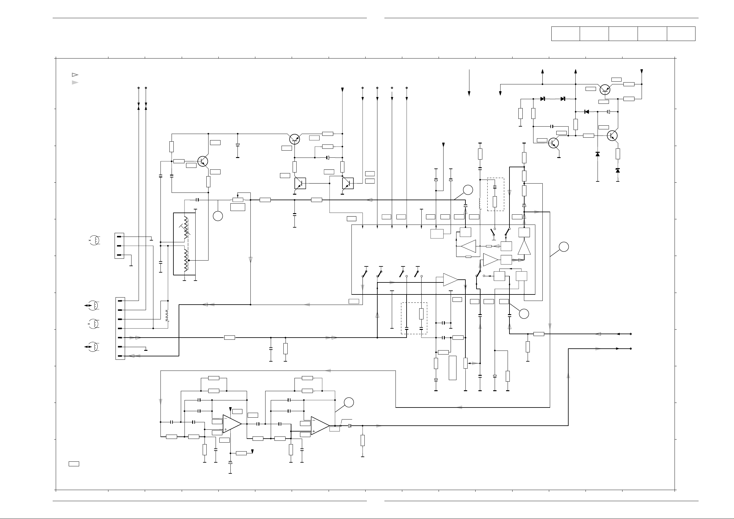
Platinenabbildungen und Schaltpläne / Layout of PCBs and Circuit Diagrams TVR 3710 …, TVR 5100 …, TVR 5500 … Platinenabbildungen und Schaltpläne / Layout of PCBs and Circuit Diagrams TVR 3710 …, TVR 5100 …, TVR 5500 …
Reference
AL ..............P 4-65
BUPI ..........P 4-68
CO .............P 4-43
DE..............P 4-49
IO...............P 4-59
OHA...........P 4-69
PLSP .........P4-19
PSSP2.......P 4-37
TU2............P 4-55
T
ube PCB
...P 4-33
TV..............P 4-51
TXT............P 4-58
VS..............P 4-61
Signal-Chassis – Standardton / Standard Sound (AL)
Record
A
B
C
D
E
Playback
MEH
to Deck L8to Deck L3
F
G
H
I
J
K
CTL
AEH
R/P
..V MEASURED IN PLAYBACK MODE
..V MEASURED IN RECORD MODE
MEH2
MEH1
CTL1
CTL2
AEH1
AEH2
APH
ARH
F7
1900
F8
1901
3
2
1
GNDAL
7
6
5
4
3
2
1
to DE
CTL1
CTL2
CTL1
GNDAL
GNDAL
CTL2
2621
2622
GNDAL
45671 8 9 10 11 12 13 14 15 1623
0.3V
2618
330p
GNDAL
7603
BC817-40
1E5
3619
6,2V
0V
0.1V
47k
3620
3622
0.3V
10E
0.6V
47n
1n
2620
6
11
4
27n
5602
3
330u
2651
150p
3652
68k
5603
2
1
GNDALGNDAL
ERASE & BIAS OSCILLATOR
REC
PLAY
3650
68k
3651
68k
2653
150p
2660
150p
2652
150p
3653
68k
3,7V
3,6V
2M2
2661
3658
GNDAL GNDAL
GNDAL GNDAL
2
3
-6V
27p
GNDAL
3618
BIAS
3600
47E
+12A
8
4
TL072CN
2654
GNDAL
2619
100k
12V
16V
100u
7608
3661
10E
16V
47u
1
3,7V
2655
150p
3654
-7V
3617
22k
GNDAL GNDAL
68k
7604
BC328-40
1n
2600
2656
150p
3655
12V
10k
2626
10n
3660
68k
3656
68k
3,5V
10V
3608
470E
6
TL072CN
5
12V
9.4V
3623
12V
0.3V
7605
DTC124EK
GNDAL GNDAL
GNDAL
100k
3601
2658
150p
2657
150p
3,4V
68k
27p
2M2
2662
3657
47u
7608
3625
33E
3624
3k3
2617
0V
8.2V
16V
7
3,5V
+12A
10k
3621
AUDIO
2u2
7606
DTC124EK
5,6V
EE/PB
8
2659
50V
from DE
LPA
MTA
IPAL
IREC
IREC
IPAL
5V
0,3V
0V
EE/PB
REC/EE
CTL
REC
1
23456789
100k
3659
GNDAL
MTA
MUTE
CTL CTL
GNDAL
LPA
EP
EP
2601
GNDAL
2021222324
LPEPRIPPLE
CTL
7601
LA7282
330E
3602
for LP only
1n5
2602
0.5V0V
100n
GNDAL
2616
FILTERCTL
used
100E
3605
2605
+12A
16V
47u
9.1V12V0V0V
2630
not
2604
10n
3604
390k
16V
100u
GNDAL
16V
2615
47u
4.3V 1.4V
EQ
7,1V
3.9V
GNDAL
3603
12k
PB-LEVEL
from TV
-7V
GNDAL GNDAL
220E
3616
12n
2613
10
2614
171819
POWER
MUTE
AMP
50V
1u
1.5V4.2V
PB
2612
3615
10m
5601
AMP
REC
EE
10 11 12
0.6V 3.8V3.9V
0V
100n
2606
PLAY
10k
3606
2n2
2608
2609
GNDAL
+12A
33n
390E
for LP only
3.8V
3.9V
REC
EP
LP
EE
MUTE
MUTE
ALC
100n
2607
16V
1M
3607
47u
GNDALGNDALGNDALGNDAL
REC*E/E*PLAY
100E
3696
GNDAL
3614
3613
3612
2611
13141516
POWER
MUTE
BUF
ALC
DET
9
to IO
+12A +12A +14M1S
7690
14,5V
BDC02D
12V
10k
2k2
12k
6690
BZX79-C8V2
100E
3695
0,7V
BZX79-C3V0
2691
15p
GNDAL
6691
7,7V
7692
BC848B
3694
1k
6692
1N4148
3697
390E
6694
13,8V
47u
7,7V
1N4148
2690
16V
6693
GNDALGNDAL
50V
2u2
12
REC*E/E*PLAY
from/to IO
10k
3610
GNDAL
3611
33k
REC
13,8V
7691
BC848B
3692
560E
7,5V
from TVto TV,TU2
3690
4E7
3691
330E
BZX79-C5V1
AMLR
AMLP
1900 F 2
1901 H 2
2600 H 6
2601 G10
2602 G10
2604 H11
2605 I10
A
2606 G12
2607 G12
2608 I12
2609 I12
2611 D13
2612 D12
2613 C12
2614 D11
2615 C11
2616 C10
2617 C 7
2618 D 4
B
2619 B 5
2620 C 3
2621 C 3
2622 F 3
2626 D 7
2630 G11
2651 J 3
2652 J 4
2653 I 4
2654 K 5
C
2655 J 6
2656 J 6
2657 J 6
2658 I 6
2659 J 8
2660 J 4
2661 K 4
2662 K 7
2690 B15
2691 B14
D
3600 H 5
3601 H 6
3602 G10
3603 H11
3604 H11
3605 H10
3606 H11
3607 I12
3608 D 7
3610 H13
E
3611 H13
3612 D13
3613 C13
3614 C13
3615 D12
3616 C12
3617 D 6
3618 D 5
3619 C 4
3620 C 3
F
3621 C 8
3622 C 3
3623 C 6
3624 B 7
3625 B 7
3650 I 4
3651 I 4
3652 J 3
3653 J 4
3654 J 6
G
3655 J 6
3656 I 7
3657 K 6
3658 K 4
3659 K 8
3660 I 7
3661 K 5
3690 A16
3691 A16
3692 C15
H
3694 B14
3695 B13
3696 B13
3697 B15
5601 D12
5602 G 3
5603 E 4
6690 A13
6691 A14
6692 B15
I
6693 C15
6694 C15
7601 E10
7603 C 4
7604 B 6
7605 C 6
7606 D 8
7608 J 5
7608 J 7
7690 A15
J
7691 B15
7692 B14
K
45671 8 9 10 11 12 13 14 15 1623
4 - 65 GRUNDIG Service 4 - 66 GRUNDIG Service
Page 76
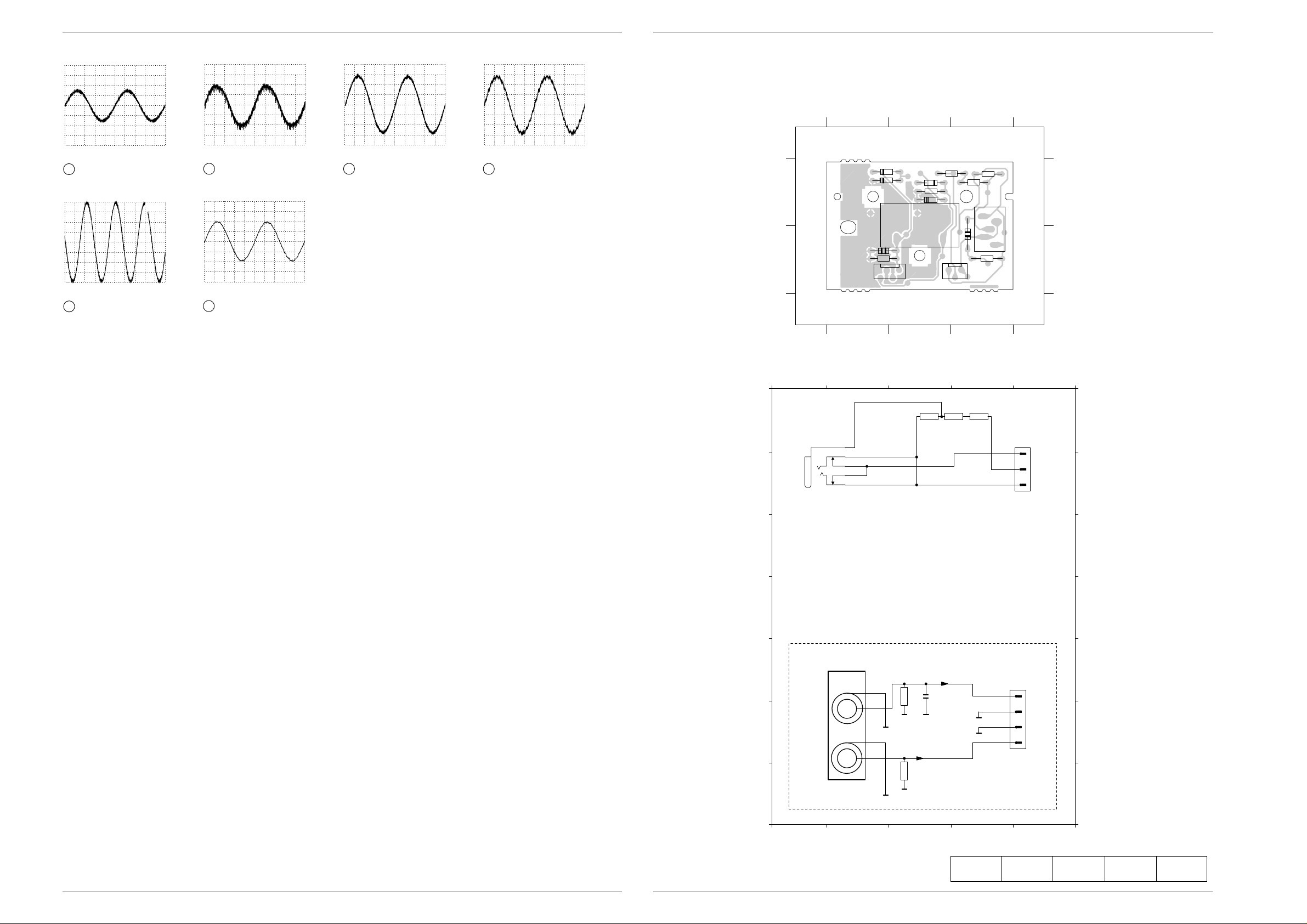
TVR 3710 …, TVR 5100 …, TVR 5500 … Platinenabbildungen und Schaltpläne / Layout of PCBs and Circuit Diagrams
123
123
B
A
B
A
1931 B 3
1933 B 2
1935 B 3
1937 B 2
2270 B 3
2272 B 1
3270 A 3
3271 A 3
3272 A 3
3273 B 3
3275 B 1
3276 A 2
6272 A 1
6273 A 1
6274 A 2
6275 A 2
1933
2272
3275
6272
6273
1937
1931
3270
1935
3271
3272
3273
6274
6275
3276
2270
Reference
AL ..............P 4-65
BUPI ..........P 4-68
CO .............P 4-43
DE..............P 4-49
IO...............P 4-59
OHA...........P 4-69
PLSP .........P4-19
PSSP2.......P 4-37
TU2............P 4-55
T
ube PCB
...P 4-33
TV..............P 4-51
TXT............P 4-58
VS..............P 4-61
CONN 1918
to PSSP2 (IO-Part)
from PSSP2 (TV-Part)
CONN 1971
Headphone Jack
for CINCH-AV only
PH1
PH2
PH3
ACIM
GND
GND
VCI
3276 G 3
3275 E 3
3272 A 4
3271 A 4
3270 A 3
2272 E 3
1937 E 4
1935 A 5
1933 E 2
1931 A 1
4512 3
E
D
C
B
A
G
F
E
D
C
B
A
G
F
4512 3
3276
75E
3270
82E
3271
47E
3275
100k
3272
47E
1933
AUDIO
VIDEO
GNDA
GNDV
AUD
VID
AV CINCH
1931
HSJ1406
1
2
3
4
5
1935
1
2
3
2272
470p
1937
1
2
3
4
REC
PB
REC
REC
TVR 3710 …, TVR 5100 …, TVR 5500 … Platinenabbildungen und Schaltpläne / Layout of PCBs and Circuit Diagrams
Buchsenplatte / Socket Board (BUPI)
Ansicht von der Bestückungsseite / View of Component Side
AC, 500mV/Div, 200µs/Div
IC7608-(7)
8
AC, 20V/Div, 5µs/Div
C2618
11
REC
AC, 200mV/Div, 200µs/Div
IC7608-(7)
8
AC, 100mV/Div, 200µs/Div
IC7601-(13)
12
REC
AC, 100mV/Div, 200µs/Div
IC7601-(11)
9
AC, 500mV/Div, 200µs/Div
IC7601-(17)
10
GRUNDIG Service 4 - 67
GRUNDIG Service 4 - 68
Page 77
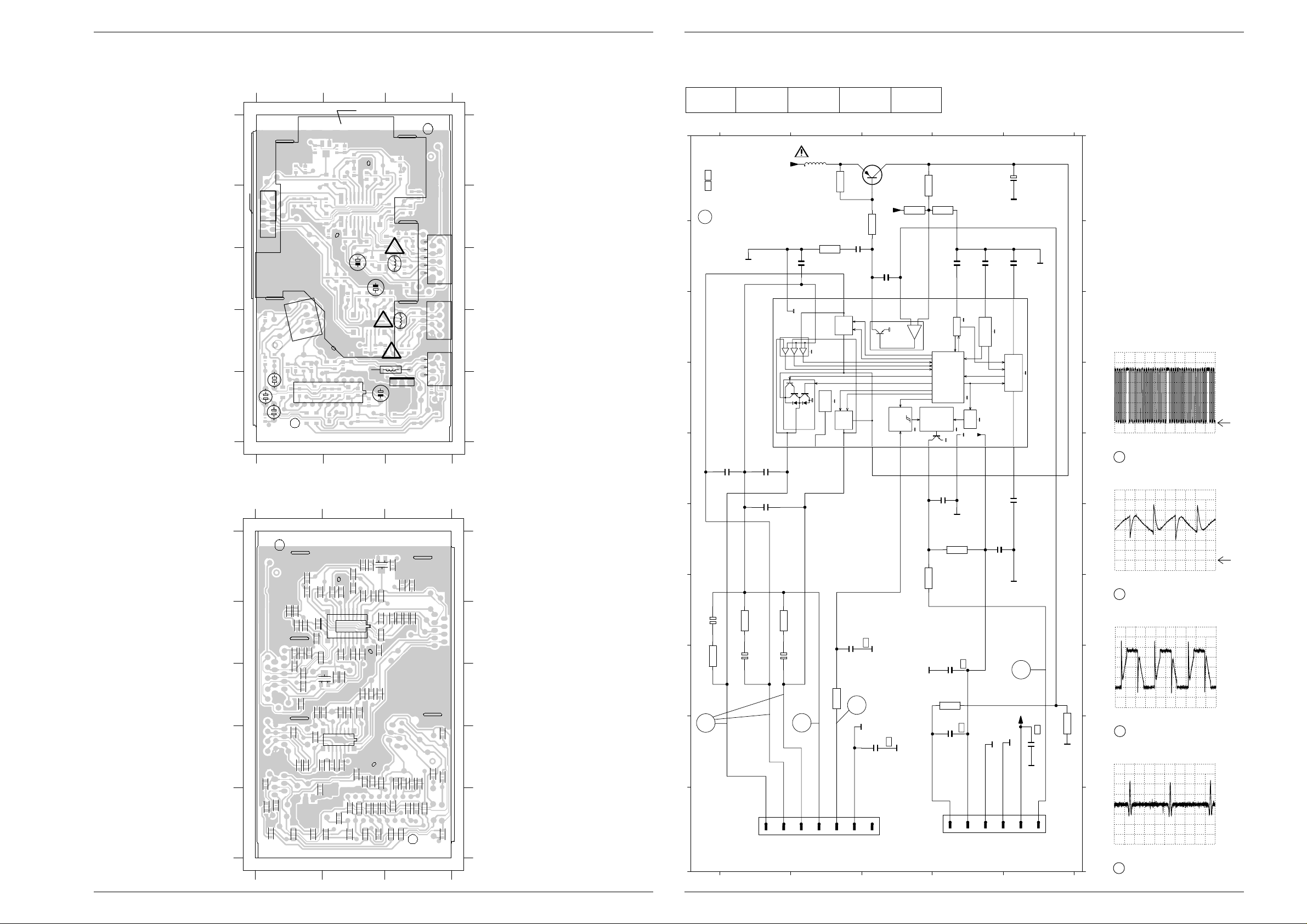
Platinenabbildungen und Schaltpläne / Layout of PCBs and Circuit Diagrams TVR 3710 …, TVR 5100 …, TVR 5500 … Platinenabbildungen und Schaltpläne / Layout of PCBs and Circuit Diagrams TVR 3710 …, TVR 5100 …, TVR 5500 …
DC, 1V/Div, 10ms/Div
0V
Connectors 1904-(1), 1930-(6)
REC
23
DC, 1V/Div, 500µs/Div
0V
Connector 1931-(4)
80
PB
DC, 2V/Div, 2ms/Div
Connector 1931-(1…3)
81
PB
AC, 100mV/Div, 10ms/Div
Connetor 1931-(5)
82
PB
8
23
82
80
81
0
0
0
4
4
NOT USED
ONLY FOR 4/X
0
4
..
OHA (...3922.4)
DE 1904
HMO1
HMO0
HMO3
POS
HMO2
TO SCANNER MOTOR TO SIGNAL CHASSIS
REEL
+5D
GNDM2
GNDD
+14M1
PG/FG
GNDD
OSCILLOGRAMS
7302 A 3
7301 D 5
5301 A 3
3314 A 4
3313 I 6
3312 H 5
3311 A 4
3310 A 5
3309 A 3
3308 B 4
3307 B 3
3306 F 5
3305 G 4
3304 G 2
3303 H 1
3302 G 2
3301 H 3
2320 I 6
2319 B 3
2318 E 2
2317 E 2
2316 E 2
2315 G 3
2314 A 6
2313 B 6
2312 B 5
2311 B 5
2310 B 3
2309 B 4
2308 E 6
2307 F 5
2306 E 5
2305 H 2
2304 G 1
2303 H 2
2302 I 5
2301 I 4
2300 H 5
1931 J 4
1930 J 4
45623
G
F
E
J
D
C
B
A
I
H
G
F
E
J
D
C
B
A
I
H
456
1
12 3
1931
7
6
5
4
3
2
1
GNDD
GNDD
GNDD
GNDD
GNDM2
GNDD
GNDM2
GNDD
GNDM2
GNDD
GNDA
GNDA
GNDA
2315
10n
2316
22n
2317
22n
2318
22n
2306
100p
2307
100n
2308
10n
2309
100n
2310
10n
2311
10n
2312
47n
2313
22n
2319
22n
2301
100p
2302
22n
2300
470p
2320
220p
+14M2
+14M1
+14M2
3304
100E
3310
1k
3305
1k
3306
4k7
3307
47E
3308
470E
3311
3k9
3302
100E
3303
100E
3312
0E
3313
15k
3301
270E
3314
39k
1930
6
5
4
3
2
1
1u
2305
1u
2303
1u
2304
330n
5301
2314
2u2
7301
15
910
11
12
18717
1
316
6
5
2
4
13
14
PROTECT
THERMAL
DEVIDE
BY 2
STAGE2
DRIVER
OUTPUT
STAGE1
DRIVER
OUTPUT
FLYBACK
PUSH/PULL
ROTATION
POSITION
SPEED &
DETECTOR
STAGE
OUTPUT
STAGE
POSITION
DETECTOR
PG/FG
GND2
VCC
CAP_CD
VMOT
MOT2
TEST
MOT1
PG_IN
ADAPTIVE
COMMUNICATION
DELAY
COMMUNICATION
LOGIC
AMPLIFIER
DUCTANCE
TRANSCON-
START-UP
OSCILLATOR
TIMING
STAGE3
DRIVER
OUTPUT
+AMP_IN
-AMP_IN
AMP_OUT
CAP-ST
CAP_DC
CAP_TI
MOT3
MOT0
GND1
-
+
TDA5140A
7302
BD436
3309
470E
L1
Reference
AL ..............P 4-65
BUPI ..........P 4-68
CO .............P 4-43
DE..............P 4-49
IO...............P 4-59
OHA...........P 4-69
PLSP .........P 4-19
PSSP2.......P 4-37
TU2............P 4-55
T
ube PCB
...P 4-33
TV..............P 4-51
TXT............P 4-58
VS..............P 4-61
Kopfverstärkerplatte / Head Amplifier Board (OHA) Kopfverstärkerplatte – Kopfscheibenmotoransteuerung
Ansicht von der Bestückungsseite / View of Component Side
Ansicht von der Lötseite / View of Solder Side
4 - 69 GRUNDIG Service 4 - 70 GRUNDIG Service
123
A
0006
1911
0007
B
C
D
E
1912
2304
11
2026
1
1
18
18
2106
!
!
5301
E
1
1
9
3
1
9
2305
9
10
10
2303
103 39220
123
7301
3017
2013
30073008
3107
3105
3311
2002
3002
3016
2011
3010
2012
3097
3009
2010
3103
3104
3308
2006
3094
3095
7021
2108
2102
2101
3309
2008
7050 7051
3099
7150
3102
2319
2310
3018
2005
7052
2014
3011
2112
3101
2003
2004
3093
2109
2317
3307
2021
3098
2007
3012
3813
2110
2301
2315
3313
2318
3312
7020
3021
3091
2009
2103
3305
3310
2309
3092
3006
3003
3812
3301
2311
A
B
C
D
E
2320
2302
2300
3314
OHA
6192. 2
3015
!
5002
5101
C
B
7302
2314
OHA
6194. 2
111
1
1910
1920
11
1930
OHA
6192. 2
123
3020
3001
2001
3004
3005
3013
3014
2316
3304
3303
2307
2308
3306
2306
3096
3833
2313
2312
3831
3832
3302
103 39220
123
1910, 1930 —> Signal Chassis (1902, 1904)
1911, 1912 —> Bandtrommel / Headwheel
0006 A 2
1910 C 3
1911 B 1
1912 B 1
1920 D 3
1930 D 3
1931 D 1
A
2026 C 2
2106 C 2
2303 E 1
2304 E 1
2305 E 1
2314 E 2
5002 C 3
5101 D 3
5301 D 3
B
7301 E 2
7302 E 3
C
D
E
A
B
C
D
E
2001 A 1
2002 A 3
2003 A 2
2004 A 2
2005 A 2
2006 A 3
2007 A 2
2008 A 2
2009 B 2
2010 C 3
2011 B 3
2012 B 3
2013 B 3
2014 B 2
2021 A 2
2101 D 3
2102 C 3
2103 C 2
2108 C 2
2109 C 2
2110 C 2
2112 C 2
2300 E 3
2301 D 2
2302 E 3
2306 D 1
2307 D 1
2308 D 1
2309 E 2
2310 E 2
2311 E 2
2312 E 1
2313 E 1
2315 D 2
2316 D 1
2317 E 2
2318 E 2
2319 E 2
2320 D 3
3001 A 1
3002 A 3
3003 B 2
3004 B 1
3005 B 1
3006 B 2
3007 B 3
3008 C 3
3009 C 3
3010 B 3
3011 C 2
3016 B 3
3017 B 3
3012 B 2
3013 B 1
3014 B 1
3015 B 3
3018 A 2
3020 A 1
3021 A 2
3091 A 2
3092 A 2
3093 B 2
3094 B 3
3095 B 3
3096 E 1
3097 C 3
3098 A 2
3099 C 2
3101 D 2
3102 D 2
3103 D 3
3104 D 3
3105 D 3
3107 D 3
3301 D 2
3302 E 1
3303 D 1
3304 D 1
3305 D 2
3306 D 1
3307 E 2
3308 E 3
3309 E 3
3310 E 2
3311 E 3
3312 E 2
3313 E 2
3314 E 3
3812 C 2
3813 C 2
3831 E 1
3832 E 1
3833 E 1
7020 A 2
7021 C 2
7050 B 2
7051 B 2
7052 B 2
7150 D 2
Head Amplifier Board – Headwheel Motor Control
Page 78
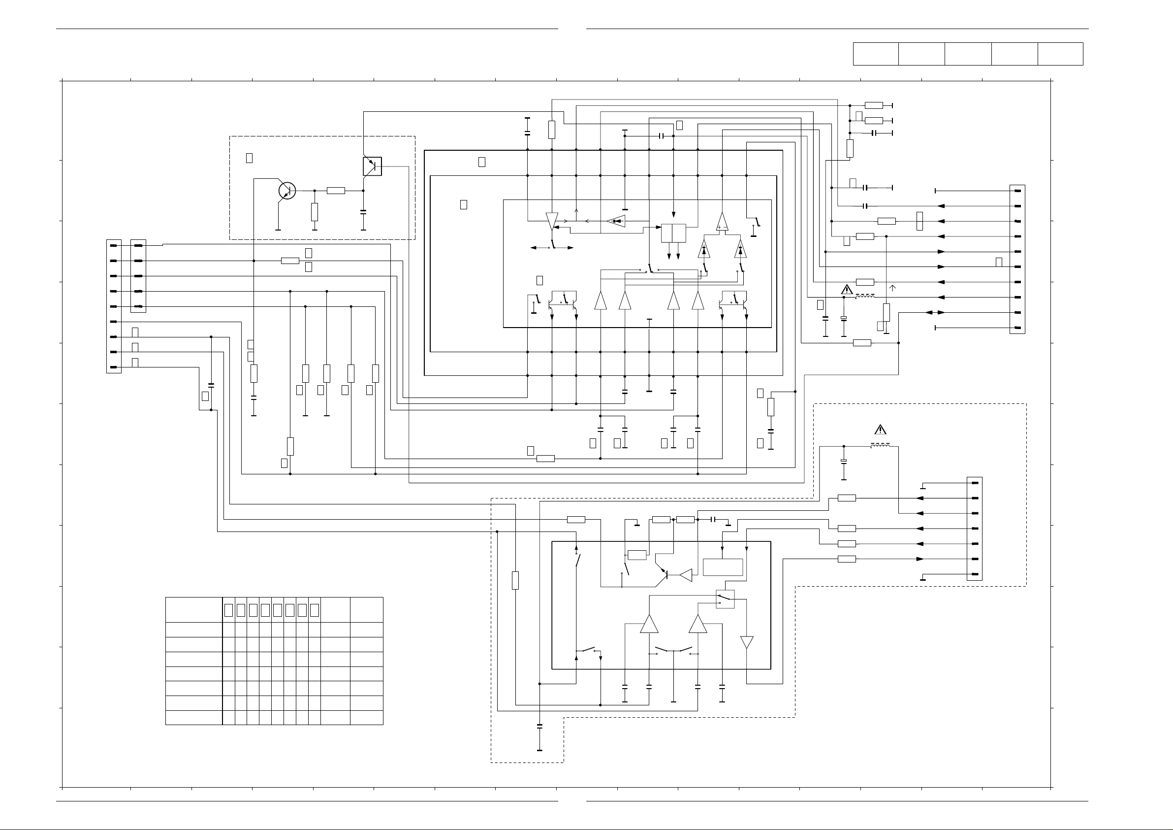
TVR 3710 …, TVR 5100 …, TVR 5500 … Platinenabbildungen und Schaltpläne / Layout of PCBs and Circuit Diagrams
Reference
AL ..............P 4-65
BUPI ..........P 4-68
CO .............P 4-43
DE..............P 4-49
IO...............P 4-59
OHA...........P 4-69
PLSP .........P4-19
PSSP2.......P 4-37
TU2............P 4-55
T
ube PCB
...P 4-33
TV..............P 4-51
TXT............P 4-58
VS..............P 4-61
Kopfverstärkerplatte – Kopfverstärker
Head Amplifier Board – Head Amplifier
451 6 7 8 9 101112131415 1623
A
2k2
3012
22n
2009
16
15
REC
IN
20
19
REC
IN
20
19
REC
IN
4
REC
V1
1
2
V1
1
2
V1
1
4
3006
0E
100n
2112
B
TO ROTATING TRANSFORMER
1912
SH1
VH1
C
D
E
VHC
VH2
VH1'C
VH1'
SHC
SH2
LH2
LHC
LH1
AH2
AHC
AH1
F
G
H
I
J
9
8
7
6
5
4
3
2
1
1911
5
4
3
2
1
6
6
6
2103
0
VARIANT
OHA 2/0
OHA 2/0
LP
OHA 3/0
OHA 4/0
OHA 2/2
OHA 3/2
OHA 4/2
220p
01
5
2
560E
5
330E
3001
10n
2001
4
3
2
X
X
X
X
X
X
7020
BC818-40
3092
3013
7
0E
3014
7
56
X
X
X
XXX
X
X
DTA124EK
7021
3021
3k9
22k
3020
5
33E
0E
2
0E
0E
3003
33
1911
7
1912
5 pin
5 pin
5 pin
9 pin
9 pin
9 pin
9 pin
2021
0E
3004
4
3015
15k
18k
12k
18k
18k
18k
18k
100n
3005
STV5742
2
CAGC
REC
7052
CAGC
STV5743
7051
3
REC
CAGC
REC
I_OUT
SP
STV5744
7050
SP
I_OUT H1
I_OUT H3
0E
I_OUT C2
0E
3813
TVR 3710 …, TVR 5100 …, TVR 5500 … Platinenabbildungen und Schaltpläne / Layout of PCBs and Circuit Diagrams
2
2014
22n
10
14
GND2
CSYN
TRIV
17
18
CSYN
TRIV
17
18
GND2
CSYN
TRIV
I_OUT
LP
VCC
SPSP
V2
3
V2
3
V2
3
2
3812
0E
16
V1 SW-H
SP LPLP
H2
H2
4
H2 NC
NC
4
H2
C1
2003
4
54
2007
10n
2004
22
15
IOUT
YCPB
SWR
16
YCPB
SWR
16
YCPB
SWR
GND1
5
GND1
5
GND1
10n
10n
14
GND2
PROT
VCC
15
VCC
15
VCC
SP/LP H1/H2
H1
6
H1
6
H1
6
2008
2005
3101
8E2
13
PROT
11
12
13
SWIN
14
SWIN
14
SWIN
LPSP
7
7
10n
10n
2006
5
3102
680E
12
VMES
9
13
NCGND2
13
ENVC
8
8
87
10n
2101
22p
11
VIN
SW LOGIC
STV5712
7150
C2
V2
VCC
1
H2
3
2
10n
2109
10n
2110
GND1
54
2108
H1
6
10n
1910 B16
1911 C 2
3015
1%
3017
0
2013
10n
10k
3016
11
12
NC
11
12
I_OUT
LP
VCC
REC
0
LP
V2
V1
10
9
V3
10
9
2011
0
5
10n
47u
2026
2012
10p
2010
10n
3008
4k7
3009
56k
5002
47u
3011
100E
3015 SEE VARIANT - TABLE
TO SMALL SIGNAL BOARD
3007
3010
0
2
4k7
5
10k
LP=H
LP>SP=H
H=AGC REC
=SP/LP TRIG
REC=H
VS 1902
SH1=H
LH2=H
VH1/VH1'=H
4
L6
10
GNDA
9
FMRV
8
HP1
7
HSC
6
TRIV
ENVC
5
4
CSYNC
3
+5A
FMPV
2
REV
1
GNDA
4
330E
3002
ONLY FOR FM-AUDIO
10n
10
SW-
REC
2002
4
9
2106
3103
1k
3104
4k7
3105
4k7
3107
100E
5101
47u
47u
( OHA X/2 )
TO SMALL SIGNAL BOARD
REC=H
AH1=H
AF 1905
1920
7
6
5
4
3
2
1
GNDA
FMAR
+5A
RAF
HP2
FMAP
GNDA
1912 C 1
1920 G15
2001 E 3
2002 F12
2003 F 9
A
2004 F10
2005 F10
2006 F11
2007 E10
2008 E10
2009 A 8
2010 B14
2011 D13
2012 B14
2013 A14
2014 A10
B
2021 B 5
2026 D13
2101 G11
2102 J11
2103 E 3
2106 F13
2108 J11
2109 J10
2110 J10
2112 K 8
C
3001 E 3
3002 F12
3003 E 5
3004 E 5
3005 E 5
3006 F 8
3007 B14
3008 C14
3009 C14
3010 D14
D
3011 D14
3012 A 8
3013 E 4
3014 F 4
3015 A14
3016 A13
3017 A14
3020 B 4
3021 B 5
3092 C 4
E
3101 G10
3102 G11
3103 G13
3104 G13
3105 H13
3107 H13
3812 G 9
3813 H 8
5002 D14
5101 F14
F
7020 B 4
7021 B 5
7050 C 8
7051 B 6
7052 B 6
7150 I 9
G
H
I
FMOUT
C1
2102
87
10n
J
K
451 6 7 8 9 101112131415 1623
GRUNDIG Service 4 - 71
K
OHA (...3922.4)
HA-ECO
GRUNDIG Service 4 - 72
Page 79
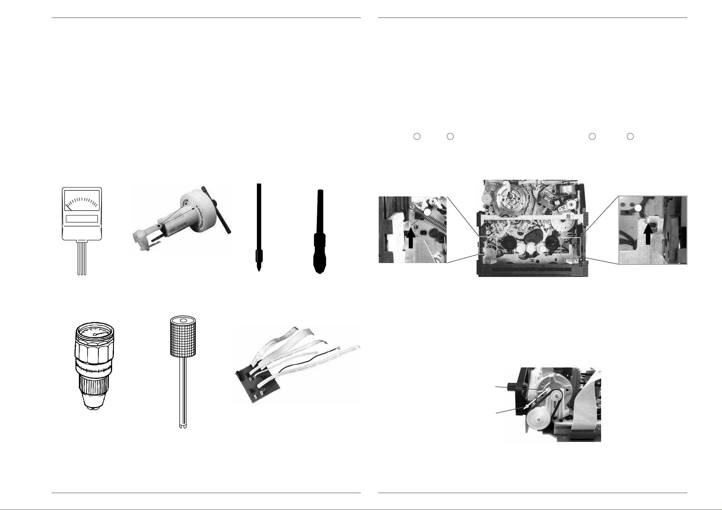
Laufwerk / Drive Mechanism TVR 3710 …, TVR 5100 …, TVR 5500 …
Laufwerk / Drive Mechanism TVR 3710 …, TVR 5100 …, TVR 5500 …
Laufwerk
Das Laufwerk besteht aus 3 Motoren:
– Präzisionsantrieb der Kopfscheibe
– Direktantrieb der Capstanwelle und der Wickelteller
– Motor für die Cassettenschachtbewegung und das Ein-/Ausfädeln
des Bandes.
Besondere Merkmale sind:
– Quickstart
– Kurze Umspulzeit
– Automatische Reinigung der Videoköpfe durch Reinigungsrolle.
Um zuverlässige Reparaturen zu garantieren, wurde eine Anzahl von
Service Kits (A, B, C …) entwickelt. Diese Kits enthalten alle wesentlichen Ersatzteile, die miteinander im Eingriff stehen.
Die angegebenen Positionsnummern (Pos. …) sind auch in den
Explosionszeichnungen angegeben.
Meßgeräte / Meßmittel
Sach-Nr.
Testcassette 9.27540-1011
Testcassette (HiFi) 9.27540-1016
Nylonhandschuhe handelsüblich
Drive Mechanism
The tape deck is fitted with three motors providing:
– Precision drive for the headwheel
– Direct drive for the capstan and the reels
– Drive for the cassette compartment and tape threading/unthreading
operations.
Special features are:
– Quick start
– Short winding time
– Automatic cleaning of video heads with a cleaning roller.
To obtain a high repair standard we have developed a range of service
kits (A, B, C …). These kits cover all important spare parts which
engage with each other.
The position numbers (Pos. …) in this description are also specified in
the exploded views.
Test Equipment / Jigs
Part no.
Test cassette 9.27540-1011
Test cassette (HiFi) 9.27540-1016
Nylon gloves commonly available
1. Servicehinweise
Zu den Servicearbeiten am Laufwerk empfehlen wir zusätzlich den
Video-Lehrfilm, Sach-Nr. 72007-744.81.
Da die meisten Teile des Laufwerkes nur mit Schnapphaken befestigt
sind, werden im folgenden nur die wesentlichen Teile beschrieben. Mit
Schrauben sind nur befestigt:
– Cassettenschacht
– Scanner
– Capstanmotor
– Kombikopf.
Anmerkung:
Bei einer Änderung der Position des Cassettenschachtes (Lift) während der Reparatur muß dieser danach von Hand in die Position "Eject"
gebracht werden.
1.1 Absenken des Cassettenschachtes von Hand (ohne Cassette)
– Gerät vom Netz trennen.
– Arretierungen R (Fig. 1) und S (Fig. 2) des Cassettenschachtes
lösen und diesen dabei so weit nach innen schieben, bis sich der
Cassettenschacht leicht absenkt.
– Fädelmotor entgegen dem Uhrzeigersinn drehen (Fig. 3), bis der
Cassettenschacht abgesenkt ist.
1. Service Instructions
When repairing the drive mechanism we recommend that the video
training film, part no. 72007-744.81.
Due to the fact that most of the components are secured with snap
hooks only the important parts will be described in the following. The
only parts fastened with screws:
– cassette compartment
– scanner
– capstan motor
– A/C (combi) head.
Advice:
When changing the position of the cassette compartment (lift) during
repairs, the compartment must be moved manually to the "Eject"
position on completion of the repairs.
1.1 Lowering the Cassette Compartment by Hand (without cass.)
– Disconnect the video recorder from the mains.
– Release the locks R (Fig. 1) and S (Fig. 2) of the cassette
compartment and move it inwards until the cassette compartment
lowers by a small amount.
– Turn the threading motor counterclockwise (Fig. 3) until the cassette
compartment is down.
T e n t e l o m e t e r
Bandzugmesser
Tentelometer
handelsüblich / commonly available
Kopfscheibenabzieher
Headwheel extractor
Sach-Nr. / Part no. 75988-002.37
Bandzug-Einstellstift und -griff
Tape tension adjustment tool - pin and handle
Sach-Nr. / Part no. 75988-002.27
R
Fig. 1 Fig. 2
1.2 Cassettenauswurf von Hand
Wenn nach dem Drücken der Eject-Taste das Laufwerk nicht ausfädelt
und die Cassette auswirft, kann dies auch von Hand durchgeführt
werden. Dazu ist das Antriebsrad des Fädelmotors zu drehen (Fig. 3).
Um Bandschlaufen zu vermeiden, muß wechselweise auch der Capstanmotor (Pos. 127, Fig. 5) entgegen dem Uhrzeigersinn bewegt
werden, bis das Band komplett in der Cassette aufgewickelt ist.
S
1.2 Manual Ejection of the Cassette
If the tape deck does not unthread and eject the cassette by pressing
the Eject button this function can also be effected manually by turning
the driving gear at the threading motor (Fig 3). To avoid slackening of
the tape, turn the capstan motor (counterclockwise) (Pos. 127, Fig. 5)
and the driving gear alternately until the tape is completely wound up
in the cassette.
Einfädeln / thread
Ausfädeln / unthread
Drehmomentmesser: 600gf-cm
Torquemeter: 600gf-cm
Sach-Nr. / Part no. 75987-262.72
Adapter:
Sach-Nr. / Part no. 75987-262.73
5 - 1 GRUNDIG Service 5 - 2 GRUNDIG Service
Einstellschraubendreher
Adjustment screw driver
Sach-Nr. / Part no. 75987-262.80
Kabeladapter
Extension cable kit
Sach-Nr. / Part no. 75988-009.79
Fig. 3
Page 80
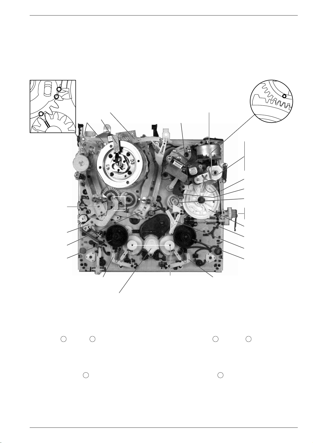
TVR 3710 …, TVR 5100 …, TVR 5500 … Laufwerk / Drive Mechanism
2. Auswechseln von Laufwerksteilen
2.1 Zahnräder- und Hebelpositionen
(Laufwerk in Stellung "ausgefädelt; Cassettenschacht unten")
Nachfolgend sind die markierten und gerichtet einzubauenden Teile
der Ober- und Unterseite im Detail dargestellt (Fig. 4, Fig. 5).
Laufwerkoberseite (Cassettenschacht abgenommen).
Reinigungshebel Fädelmotor
Cleaning roller Pos. 35 Threading motor Pos. 38
Pos. 22M
Y
Bandführung links
Roller unit left Pos. 23
Bandzughebelfreigabe
Tension crank Pos.12
Hebel komplett
Tension arm Pos. 15
Bandführung rechts
Roller unit right Pos. 26
Wickelteller
Reel Pos. 20R
2. Replacement of Tape Deck Components
2.1 Position of Gearwheels and Levers
(deck position "unthreaded, cassette compartment down")
The following diagrams show in detail the marked components and their
correctly aligned position on the top and bottom side (Fig. 4, Fig. 5).
Top of the Drive Mechanism (cassette compartment removed)
Zwischenhebel
Intermediate lever Pos. 32Q
Steuerschaft
Cam shaft Pos. 46S
Andruckrollenführung
Pressure roller guide Pos. 41S
Andruckrollenhebel
Pressure roller lever Pos. 37
Schaft mit Riemenscheibe
Shaft with pulley Pos. 47
Reversehebel
Reverse lever Pos. 31Q
Zahnrad
Gearwheel Pos. 44BS
Cass. Ladezahnräder / Feder
Cassette loader gears assy Pos.,
105L, 104L, 103L
Kurvenrad
Cam wheel Pos. 45S
Schnecke
Worm shaft Pos. 48 S
Reverse Bremse
Reverse brake Pos. 42P
Wickelteller
Reel Pos. 20aR
Bremse links
Main break left Pos. 5P
Schwenkrad
Swivelling gear Pos. 17R,19R
Zahnrad (2x)
Gearwheel (2x) Pos.18R
Bremse rechts
Main brake right Pos. 10P
Fig. 4
2.2 Aus- und Einbau des Cassettenschachtes
Ausbau:
– Gerät vom Netz trennen.
– Arretierungen R (Fig. 1) und S (Fig. 2) des Cassettenschachtes
lösen und diesen dabei so weit nach innen schieben, bis sich der
Cassettenschacht leicht absenkt.
– Antriebsrad des Fädelmotors in Drehrichtung "Einfädeln" (Fig. 3) so
weit drehen, bis das Zahnrad (Pos. 103L, Fig. 6) entriegelt ist.
– Klammer (Pos. 102L) von der Achse des Zahnrades "A" lösen
(Fig. 6).
– 4 Befestigungsschrauben A (Fig. 5) des Cassettenschachtes an
der Unterseite entfernen.
– Frontblende entfernen (Servicehinweise, Kap. 1 beachten) und
Cassettenschacht abheben.
GRUNDIG Service 5 - 3
2.2 Removal and Reassembly of the Cassette Compartment
Removal:
– Disconnect the video recorder from the mains.
– Release the locks R (Fig. 1) and S (Fig. 2) of the cassette
compartment and move it inwards until the cassette compartment
lowers by a small amount.
– Turn the driving gear of the threading motor in the "threading"
direction (Fig. 3) until the gearwheel (Pos. 103L, Fig. 6) disengages.
– Release the bracket (Pos. 102L) from the shaft of gearwheel "A"
(Fig. 6).
– Unscrew the 4 screws A (Fig. 5) on the underside of the cassette
compartment.
– Remove the front panel (observe service instructions, chapter 1)
and raise the cassette compartment to remove it.
Page 81
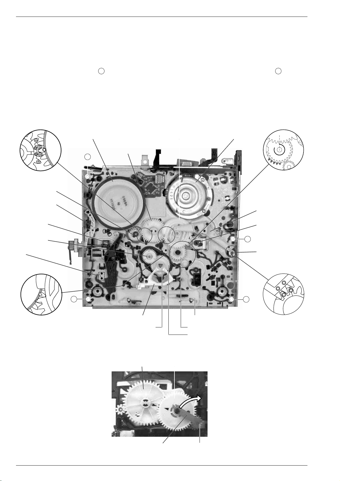
Laufwerk / Drive Mechanism TVR 3710 …, TVR 5100 …, TVR 5500 …
Zahnradpositionen für den Einbau:
– Cassettenschacht abgesenkt und Zahnrad "A" (Fig. 6) eingerastet.
Hinweis: Bei Cassettenliftzahnrädern (A und B, Fig. 6) mit Mar-
kierungspfeilen müssen die Pfeile zueinander zeigen.
– Cassettenlade-Zahnrad (Pos. 103L) ist freigegeben (ist dies nicht
der Fall, muß das Antriebsrad des Fädelmotors verdreht werden bis
es freigegeben ist).
– Cassettenschacht aufsetzen.
– Cassettenschacht mit den 4 Schrauben A (Fig. 5) unten befestigen.
– Klammer (Pos. 102L) auf der Achse des Zahnrades "A" einrasten
(Fig. 6).
Laufwerkunterseite
Capstanriemen (Pos. 126), Riemenscheibe (Pos. 128G) und Sensorplatinen-Einheit demontiert.
Capstan motor Pos. 127 Cam wheel tension Pos. 113B Scanner motor Pos. 34
Kurvenrad Reverse
Cam wheel reverse
Pos. 111B
A
Zahnrad
Gearwheel Pos. 44BS
Gearwheel Positions for Refitting the Cassette Compartment:
– Cassette compartment down, gearwheel "A" (Fig. 6) engaged.
Note: For video recorders which are fitted with cassette lift gear
wheels (A and B, Fig. 6) marked with arrows, the arrows
must show towards each other.
– Cassette loading gearwheel (Pos. 103L) is released (if it is not the
drive gear of the threading motor must be turned to release it).
– Put on the cassette compartment.
– Fasten the cassette compartment with the 4 screws A (Fig. 5) at the
bottom.
– Place the bracket (Pos. 102L) onto the shaft of gearwheel "A" and
lock it in (Fig. 6).
Bottom of Drive Mechanism
Capstan belt (Pos. 126), pulley (Pos. 128G) and sensor print assembly
removed.
Kurvenrad
Cassetten-Ladehebel
Cassette loader
lever Pos. 101L
Hebel
Cam wheel lever
Pos. 120M
Kupplung
Clutch Pos. 115
Init
A
Kupplungshebel / Clutch lever Pos. 114
Wechselzahnrad / Changing gear Pos. 116I
Steuerhebel
Tension lever Pos. 112M
Fädelrad
Loading gear Pos. 27B
A
Bandzughebelfreigabe
Tension crank Pos. 12
A
Hauptschieber / Main slider Pos. 125M
Reverse Kicker Pos. 129
Doppelrad / Double gear Pos. 117I
Fig. 5
B
A
Pos. 102L Pos. 103L
Fig. 6
5 - 4 GRUNDIG Service
Page 82
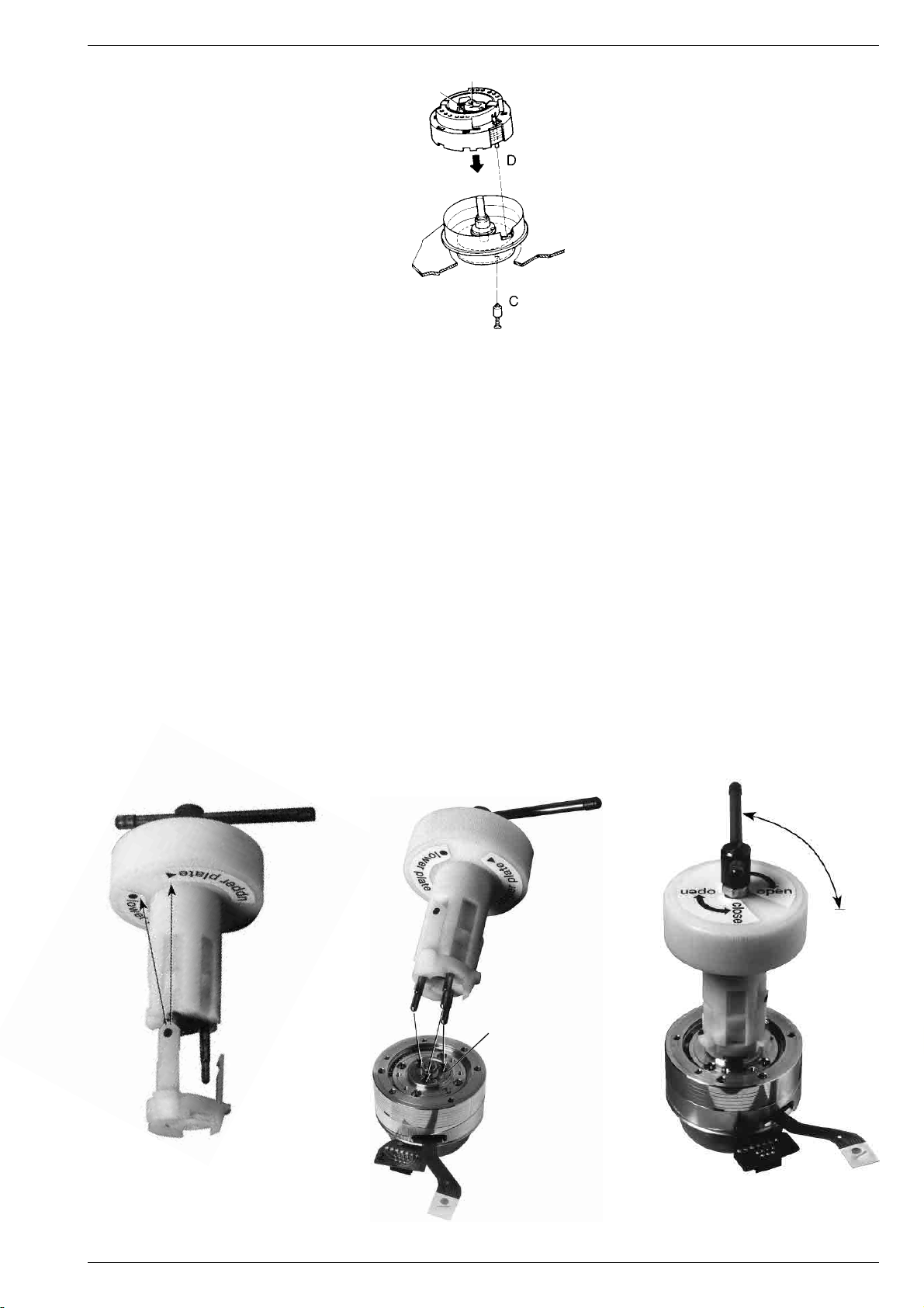
TVR 3710 …, TVR 5100 …, TVR 5500 … Laufwerk / Drive Mechanism
B
A
Fig. 7
2.3 Kopfscheibe
Hinweis: Zum Ausbau der Kopfscheibe benötigt man die Abziehvor-
richtung (Sach-Nr. 75988-002.37).
Kopfscheibe nur mit Nylonhandschuhen anfassen.
Ausbau:
– 2 Schrauben Y (Fig. 4) herausdrehen, Haltewinkel (Pos. 22M,
Fig. 4) und Kopfverstärker abnehmen.
– Referenzstift "C" (jeder Service-Kopfscheibe beigepackt) durch das
Loch im Scannermotor einschieben und die Kopfscheibe solange
verdrehen, bis dieser im Loch des Rotors einschnappt (Fig. 7).
– Abziehvorrichtung auf die Stellung "3 upper plate" (obere Klem-
mung) umstecken (Fig. 8).
– Die Abziehvorrichtung in die Kopfscheibe stecken (Fig. 9).
– Den Griff um 90° in Pfeilrichtung "OPEN" drehen und die obere
Klemmscheibe abnehmen (Fig. 10).
– Den Griff um 90° in Pfeilrichtung "CLOSE" drehen und die Klemm-
scheibe von der Abziehvorrichtung abnehmen.
– Abziehvorrichtung auf die Stellung "0 lower plate" (untere Klem-
mung) umstecken (Fig. 8).
– Die Abziehvorrichtung in die Kopfscheibe stecken (Fig. 9).
– Den Griff um 90° in Pfeilrichtung "OPEN" drehen und die Kopf-
scheibe mit der unteren Klemmscheibe abnehmen (Fig. 10).
2.3 Headwheel
Note: The extractor (part no. 75988-002.37) is necessary to remove
the headwheel.
Do not touch the headwheel with bare hands. Wear the nylon
gloves.
Removal:
– Undo 2 screws Y (Fig. 4), remove the bracket (Pos. 22M, Fig. 4) and
the head amplifier.
– Insert the reference pin "C" (delivered with each service headwheel)
into the hole of the scanner motor and turn the headwheel until the
pin locks into the hole of the rotor (Fig. 7).
– Set the extractor to the position "3 upper plate" (upper clamping
element, Fig. 8).
– Insert the extractor into the headwheel (Fig. 9).
– Turn the lever by 90° in the direction of the arrow "OPEN" and
remove the upper clamping element (Fig. 10).
– Turn the lever by 90° in the direction of the arrow "CLOSE" and
tighten the upper clamping element.
– Change the extractor to the position "0 lower plate" (lower clamping
element, Fig. 8).
– Insert the extractor into the headwheel (Fig. 9).
– Turn the lever by 90° in the direction of the arrow "OPEN" and
remove the headwheel together with the lower clamping element
(Fig. 10).
Klemmscheibe
Clamping element
Fig. 8
GRUNDIG Service 5 - 5
Fig. 9
Fig. 10
Page 83
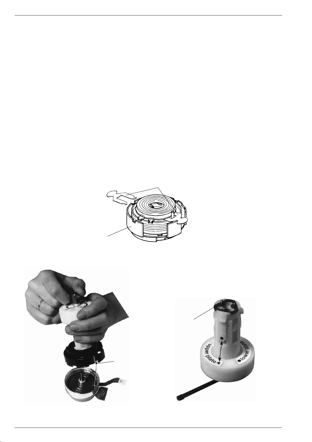
Laufwerk / Drive Mechanism TVR 3710 …, TVR 5100 …, TVR 5500 …
Einbau:
– Vor dem Einbau der neuen Kopfscheibe kontrollieren, ob die An-
triebsachse sauber und unbeschädigt ist (die Achse muß fettfrei
sein und darf nicht mit bloßer Hand berührt werden).
– Die 3 Stifte der Abziehvorrichtung durch die neue Kopfscheibe (mit
Schutzkappe) in die untere Klemmscheibe stecken (die Abziehvor-
richtung ist dabei in der Stellung "0 lower plate" (untere Klemmung).
– Den Griff um 90° in Pfeilrichtung "OPEN" drehen
– Die Kopfscheibe so aufsetzen, daß der Stift "D" der Schutzkappe in
die Bohrung des Stators eingreift. Die Kopfscheibe in der Mitte mit
einer Kraft von 1N niederdrücken und den Griff der Abziehvor-
richtung nach links in Pfeilrichtung "CLOSE" drehen (Fig. 12).
Achtung: Die obere Schutzkappe und die 2 Mylar-Abstandsfolien
(Stärke 0,15mm) bleiben bei diesem Vorgang auf der Kopfscheibe
(Fig. 11).
– Abziehvorrichtung auf die Stellung "3 upper plate" (obere Klem-
mung) umstecken (Fig. 13).
– Die Klemmscheibe auf die Stifte der Abziehvorrichtung legen
(Fig. 13) und den Griff um 90° in Pfeilrichtung "OPEN" drehen.
– Die Abziehvorrichtung mit der Klemmscheibe auf die Kopfscheibe
setzen und den Griff der Abziehvorrichtung nach links in Pfeilrich-
tung "CLOSE" drehen.
– Schutzkappe von der Kopfscheibe abziehen und die 2 Mylarfolien
seitlich aus dem Luftspalt herausnehmen.
– Referenzstift "C" von der Unterseite des Laufwerks entfernen.
Einstellungen und Kontrollen nach Austausch der Kopfscheibe:
– Kopfradlagengeber einstellen (siehe Abgleich Kap. 3).
– Aufsprechstrom einstellen (siehe Abgleich Kap. 3).
– Bandlauf kontrollieren (siehe Punkt 3.1).
Installation:
– Before fitting the new headwheel, make sure that the motor spindle
is clean and undamaged (the spindle should be free of grease and
must not be touched with bare hands).
– Put the 3 pins of the extractor into the new headwheel (with
protective cap) so that they are inserted into the lower clamping
element (the extractor is set to the position "0 lower plate")
– Turn the lever by 90° in the direction of the arrow "OPEN".
– Position the headwheel so that pin "D" of the protecting cap engages
with the hole of the stator. Press the headwheel down in the middle
with a force of 1N and turn the lever of the extractor counter
clockwise in the direction of the arrow "CLOSE" (Fig. 12).
Attention: The upper protecting cap and the 2 Mylar films (0.15mm
thick) remain on the headwheel during this process (Fig. 11).
– Change the position of the extractor to "3 upper plate" (upper
clamping element, Fig. 13).
– Place the clamping element onto the pins of the extractor (Fig. 13)
and turn the lever by 90° in the direction of the arrow "OPEN".
– Position the extractor with the clamping element on the headwheel
and turn the lever in the direction of the arrow "CLOSE".
– Remove the protecting cap from the headwheel and withdraw the 2
Mylar films laterally from the air gap.
– Remove the reference pin "C" from the bottom side of the Drive
Mechanism.
Adjustments and Checks after Replacement of the Headwheel:
– Adjust the headwheel position indicator (see adjustment, chapter 3).
– Adjust the write current (see adjustment, chapter 3).
– Check the tape transport (see para 3.1).
Schutzkappe
Protecting cap
Mylar-Abstandsfolien
Mylar distance films
Fig. 11
Klemmscheibe
Clamping element
D
Fig. 12
5 - 6 GRUNDIG Service
Fig. 13
Page 84
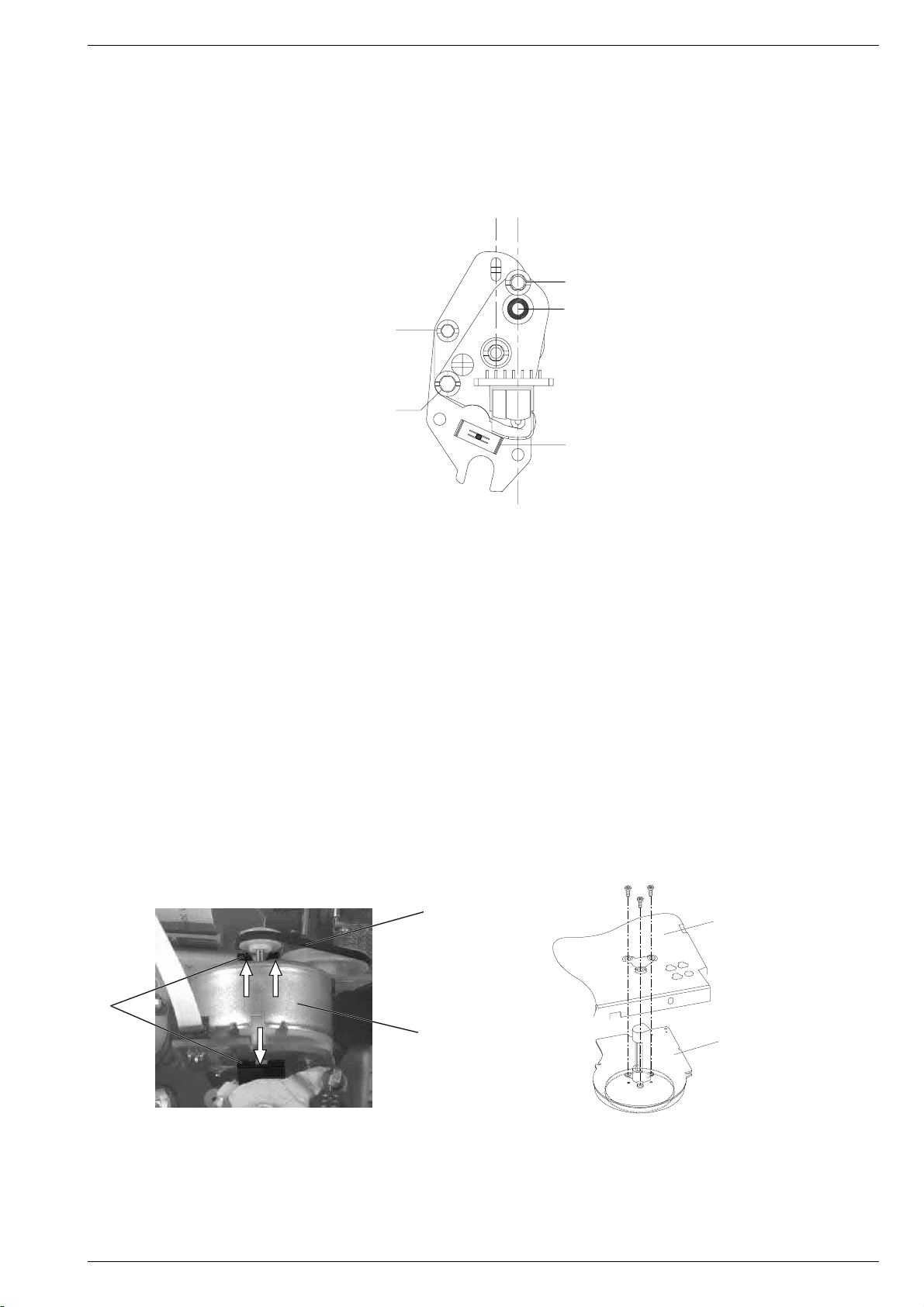
TVR 3710 …, TVR 5100 …, TVR 5500 … Laufwerk / Drive Mechanism
2.4 Kombikopf (Pos. 36)
– Befestigungsfeder "A" (Fig. 14) und den Stecker abziehen.
– Montageschraube "B" herausschrauben und den Kombikopf aus-
tauschen.
– Beim Einbau die neue beigepackte Befestigungsfeder verwenden.
Nach dem Austausch des Kombikopfes sind alle Einstellungen wie
unter Punkt 3.1.2 und Punkt 3.2 angegeben durchzuführen.
Höhen-Einstellschraube
Height setting screw
Azimut-Einstellschraube
Azimuth adjustment
screw
2.4 A/C Head (combi head, Pos. 36)
– Remove fixing spring "A" (Fig. 14) and unplug the connector.
– Undo the mounting screw "B" and replace the A/C (combi) head.
– Use the new fixing spring delivered with the replacement A/C head
for reassembly.
After the A/C head has been replaced, all adjustments described in
para 3.1.2 and para 3.2 have to be carried out.
Neigungswinkel-Einstellschraube
Tilt setting screw
Montageschraube B
Mounting screw B
A
2.5 Fädelmotor (Pos. 38)
– Antriebsriemen (Pos. 39) entfernen (Fig. 15) und den Stecker des
Fädelmotors abziehen.
– Motorhalter (Pos. 40M) in Pfeilrichtung drücken und Fädelmotor
(Pos. 38) aus dem Motorhalter nehmen (Fig. 15).
Beim Einbau darauf achten, daß der Fädelmotor vorne und hinten
eingerastet ist.
2.6 Capstanmotor (Pos. 127)
– Laufwerk in Stellung "Eject" bringen.
– Antriebsriemen (Pos. 126) entfernen.
– Sensorplatine über Capstanmotor lösen und hochklappen.
– 3 Befestigungsschrauben (Fig. 16) auf der Oberseite entfernen und
den Capstanmotor nach unten aus dem Laufwerk nehmen.
Der Einbau erfolgt in umgekehrter Reihenfolge. Zu beachten ist, daß
die Capstanwelle fettfrei sein muß.
39
Fig. 14
2.5 Threading Motor (Pos. 38)
– Remove the drive belt (Pos. 39, Fig. 15) and unplug the connector
from the threading motor.
– Press the motor support (Pos. 40M) in the direction of the arrow and
take the threading motor (Pos. 38) out of the motor support (Fig. 15).
When fitting the motor ensure that the threading motor locks into the
front and rear bearing.
2.6 Capstan Motor (Pos. 127)
– Set the tape deck to the "Eject" position.
– Remove the driving belt (pos.126).
– Release the sensor print covering the capstan motor and fold it up.
– Remove the three capstan motor fixing screws (Fig. 16) and with-
draw the capstan motor downward from the tape deck.
Reassembly is carried out in reverse order. Make sure that the capstan
is free of grease.
Chassis
40M
38
Capstanmotor
127
Fig. 15 Fig. 16
GRUNDIG Service 5 - 7
Page 85
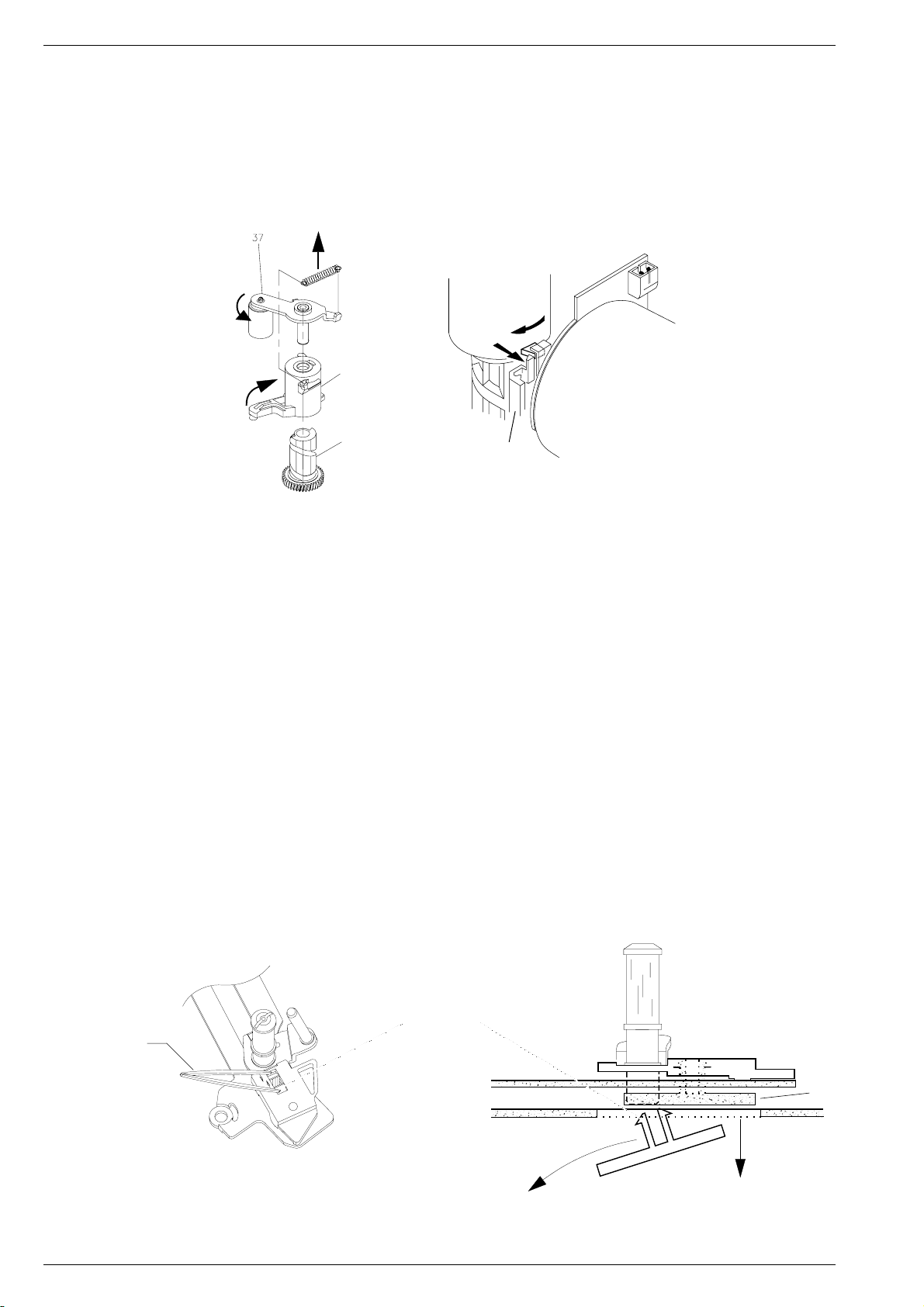
Laufwerk / Drive Mechanism TVR 3710 …, TVR 5100 …, TVR 5500 …
2.7 Andruckrolle (Pos. 37)
– Laufwerk in Stellung "Eject" bringen.
– Feder der Andruckrolle aushaken und entfernen (Fig. 17).
– Führung (Pos. 41S) aus der Nut des Fädelmotorhalters (Pos. 40)
aushaken und so weit im Uhrzeigersinn verdrehen, bis die Andruckrolle und die Führung (Pos. 41S) entriegelt und abgenommen
werden können (Fig. 17).
Achtung: Kein Fett auf die Capstanwelle bringen. Der Einbau erfolgt
in umgekehrter Reihenfolge.
41S
46S
2.7 Pressure Roller (Pos. 37)
– Set the tape deck to the "Eject" position.
– Unhook and remove the pressure roller spring (Fig. 17).
– Release the pressure roller guide (pos. 41S) from the guide in the
threading motor holder (Pos. 40) and turn the pressure roller guide
assembly clockwise until the pressure roller and the guide
(Pos. 41S) can be released and removed (Fig. 17).
Attention: Take care that the capstan does not come into contact with
grease. Reassemble in reverse order.
41G
46A
46S
41S
2
1
38
40M
Fig. 17
2.8 Fädelschlitten rechts (Pos. 26)
– Laufwerk in Position "Eject" bringen.
– Mit einer Pinzette die beiden Schnapphaken zusammendrücken
und die Umlenkrolle von der Platte (Fig. 18) abnehmen.
– Fädelarm aus der Platte aushängen und diese nach vorne aus der
Führung schieben.
Nach Austausch des Fädelschlittens rechts muß der Bandlauf
(Punkt 3.1) kontrolliert und gegebenenfalls eingestellt werden.
2.9 Fädelschlitten links (Pos. 23)
– Laufwerk in Position "Eject" bringen.
– Feder (Fig. 27, Pos. 11) aushaken, damit der Bandzugfühler nicht
vorgespannt ist.
– An der Unterseite des Laufwerks die Sensorplatine teilweise aus-
hängen und den Hebel (Pos. 112M) entfernen.
– Mit einer Pinzette die beiden Schnapphaken zusammendrücken
(Fig. 18) und die Umlenkrolle "A" von der Platte "B" abnehmen
(Fig. 19).
– Fädelarm links aus der Platte aushängen und diese durch die
Aussparung im Chassis nach unten aus dem Laufwerk entfernen
(Fig. 19).
– Der Zusammenbau erfolgt in umgekehrter Reihenfolge.
Nach Austausch des Fädelschlittens links muß der Bandlauf (Punkt
3.1) kontrolliert und gegebenenfalls eingestellt werden.
Pinzette
Tweezers
2.8 Threading Roller Unit, Right (Pos. 26)
– Set the tape deck to the "Eject" position.
– Compress the two snap hooks by means of tweezers and remove
the reverse roller from the holding plate (Fig. 18).
– Release the loading arm from the holding plate and push the latter
towards the front of the deck to remove it from the guide.
After replacing the threading roller unit (right), check and if necessary
readjust the tape transport (para 3.1).
2.9 Threading Roller Unit, Left (Pos. 23)
– Set the tape deck to the "Eject" position.
– Unhook the tension arm spring (Fig. 27, pos. 11) to avoid the tension
arm spring being pre-loaded.
– At the bottom side of the tape deck, partially unhinge the sensor print
and remove the tension lever (pos.112M).
– Compress the two snap hooks by means of tweezers (Fig. 18) and
remove the reverse roller "A" from the plate "B" (Fig. 19).
– Release the loading arm (left) from the holding plate and withdraw
the latter through the cutout in the chassis (Fig. 19).
– Reassemble in reverse order.
After replacing the threading roller unit (left) check and if necessary
readjust the tape transport (para 3.1).
A
Schnapphaken
snap hooks
B
Fig. 18
5 - 8 GRUNDIG Service
Fig. 19
Page 86
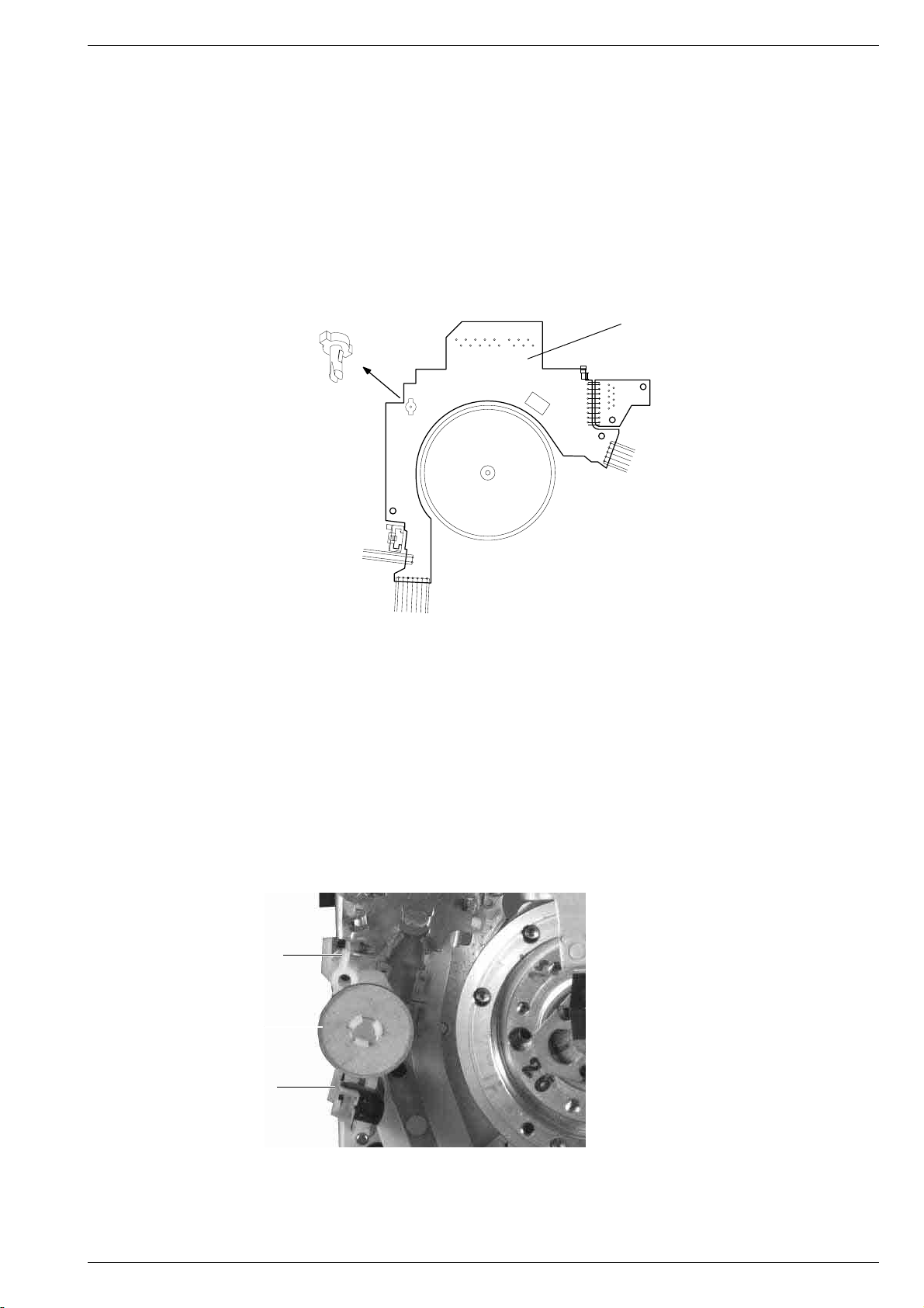
TVR 3710 …, TVR 5100 …, TVR 5500 … Laufwerk / Drive Mechanism
2.10 Laufwerkplatte–Sensoreneinheit (Pos. 118)
Bei einem Fehler auf der Laufwerkplatte–Sensoreneinheit ist diese
komplett zu tauschen:
– Rastnasen lösen (bei allen Platinen der Sensoreneinheit).
– Laufwerkplatte–Sensoreneinheit mit Spreizanker A (Fig. 20)
heraushebeln und Platinen herausnehmen.
Nach dem Einsetzen der gesamten Laufwerkplatte–Sensoreneinheit
müssen die Rastnasen eingerastet und der Spreizanker eingesetzt
sein.
Anmerkung:
Entsprechend der Laufwerksvarianten sind verschiedene Sensoreneinheiten eingebaut. Achten Sie bei der Ersatzteilbestellung darauf,
daß Sie die Sensoreneinheit für das richtige Laufwerk bestellen:
für ECO-Laufwerk: Sach-Nr. 75988-018.22,
für HSD-Laufwerk: Sach-Nr. 75988-025.06 (Sensor "7107" bestückt).
A
2.10 Tape Deck Sensor Panel (Pos. 118)
If part of the tape deck sensor panel is defective the whole panel has
to be replaced as follows:
– Release the snap hooks (all circuit boards of the sensor panel).
– Lift off the tape deck sensor panel with the expanding arbor A
(Fig. 20) and take out the circuit boards.
Reassemble the tape deck sensor panel by snapping the snap hooks
into place and by pushing in the expanding arbor.
Note:
The tape deck variants are fitted with different sensor panels. When
ordering your spare part ensure to order the correct sensor panel for
the respective tape deck:
for ECO tape deck: part no. 75988-018.22,
for HSD tape deck: part no. 75988-025.06 (sensor "7107" fitted).
Pos. 118
2.11 Beruhigungsrolleneinheit (Pos. 9)
– Befestigungshaken der Feder (a) lösen und Beruhigungsrollen-
einheit (Pos. 9) nach oben herausziehen (Fig. 21).
2.12 Löschkopfeinheit (Pos. 16)
– Beruhigungsrolleneinheit (Pkt. 2.11) ausbauen.
– Löschkopf senkrecht nach oben herausziehen (Fig. 21).
Hinweis zum Einbau: Die Löschkopfeinheit muß beim Einbau gerastet sein.
a
Pos. 9
Pos. 16
Fig. 20
2.11 Damping Roller (Pos. 9)
– Loosen the fastening hook of the spring (a) and raise the damping
roller (Pos. 9) to remove it (Fig. 21).
2.12 Erase Head Assy (Pos. 16)
– Remove the damping roller (para 2.11).
– Remove the erase head assembly in vertical direction (Fig. 21).
Note: The erase head assembly must be locked in when refitting it.
Fig. 21
GRUNDIG Service 5 - 9
Page 87
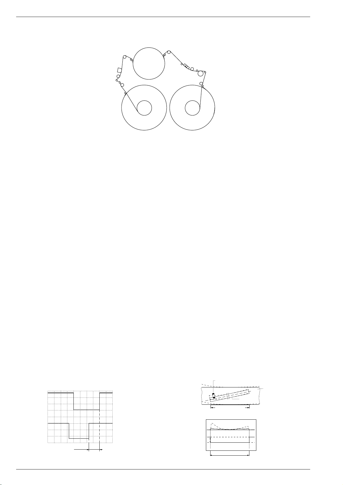
Laufwerk / Drive Mechanism TVR 3710 …, TVR 5100 …, TVR 5500 …
3. Einstellungen
3.1 Bandlauf
23
33/34
16
3.1.1 Fädelschlitten links und rechts
Grobabgleich:
– Zweikanaloszilloskop (Triggerung - Kanal A) mit den Tastköpfen
10:1 wie folgt anschließen:
• Kanal A: Kopfverstärker, Steckerkontakt 1910-(8),
Kopfumschaltimpuls "HP1".
• Kanal B: Kopfverstärker, Steckerkontakt 1910-(2),
FM-Pakete "FMPV".
– Schwarzweiß-Bild der Testcassette wiedergeben.
– Umlenkrolle des linken (Pos. 23, Fig. 22) und rechten (Pos. 26,
Fig. 22) Fädelschlittens mit dem Einstellschraubendreher so einstellen, daß die Amplitude der FM-Pakete maximal und geradlinig ist.
Feinabgleich:
Vor dem Einstellen der Fädelschlitten links und rechts muß der XAbstand (Punkt 3.2) richtig eingestellt sein. Ist dies nicht der Fall,
können die folgenden Einstellungen eine umgekehrte Wirkung zeigen.
– Zweikanaloszilloskop (Triggerung-Kanal A) mit den Tastköpfen
10:1 wie folgt anschließen:
• Kanal A: Kopfverstärker, Steckerkontakt 1910-(8),
Kopfumschaltimpuls "HP1".
• Kanal B: Chassisplatte, IC7411-(16),
Bandsynchronimpuls "CTL".
– Vor dieser Einstellung muß die Testcassette erneut eingelegt wer-
den (von Eject-Stellung starten).
– Schwarzweiß-Bild der Testcassette wiedergeben.
– Taste . drücken.
– "SPURLAGE" mit der Taste | wählen.
– Taste m CL drücken.
– Mit den Tasten x / c den Zeitabstand zwischen dem Kopfum-
schaltimpuls und der steigenden Flanke des CTL-Impulses auf
∆t = -8ms (Fig. 23) einstellen.
– Taste . drücken.
– Kanal B: Kopfverstärker, Steckerkontakt 1910-(6),
Trackingsignal "TRIV".
– Einstellung: Durch Justieren der Umlenkrolle des linken und rech-
ten Fädelschlittens (Pos. 23 und Pos. 26) mit dem Einstellschraubendreher das Trackingsignal "TRIV" auf geraden Verlauf und
minimale Abweichung einstellen (Fig. 24).
– Taste "Standby" drücken.
3. Adjustments
3.1 Tape Transport
26
29F
31F
Fig. 22
3.1.1 Threading Roller Unit Left / Right
Coarse adjustment:
– Connect the 10:1 test probes of the dual-channel oscilloscope
(channel A triggered) as follows:
• Channel A: Head Amplifier, plug contact 1910-(8),
head pulse "HP1".
• Channel B: Head Amplifier, plug contact 1910-(2),
FM-packages "FMPV".
– Play back the black/white recording on the test tape.
– Adjust the reverse roller of the left (Pos. 23, Fig. 22) and right (Pos.
26, Fig. 22) threading roller unit to obtain the maximum amplitude of
the FM-packages with straight-lined envelope.
Fine adjustment:
Before setting the left and the right threading roller units the X-distance
(para 3.2) must be adjusted correctly otherwise the following adjustments may produce an adverse effect.
– Connect the 10:1 test probes of the dual-channel oscilloscope
(channel A triggered) as follows:
• Channel A: Head Amplifier plug contact 1910-(8),
head pulse "HP1".
• Channel B: Family Board IC7411-(16),
tape sync pulse "CTL".
– Before this adjustment, take out and reload the test cassette (start
from Eject position).
– Play back the black/white recording on the test tape.
– Press the . button.
– Select "TRACKING" with button |.
– Press the button m CL.
– Using the x / c buttons set the time interval between the head
pulse and the rising edge of the CTL pulse to ∆t = -8ms (Fig. 23).
– Channel B: Head Amplifier, plug contact 1910-(6),
tracking signal "TRIV".
– Adjustment: With the adjustment screw driver set the reverse roller
of the left and right threading roller units (Pos. 23 and Pos. 26) to
make the tracking signal "TRIV" as straight and flat as possible
(Fig. 24).
– Press the "Standby" button.
Videokopf
Video head
Videospur
HP1
Video Track Diagram
CTL
∆t = -8ms
Fig. 23
5 - 10 GRUNDIG Service
Video track
Spurbild
20ms
Band
Tape
Ansicht von der Bandoberseite
View to foil side
TRIV
HP1
Fig. 24
Page 88
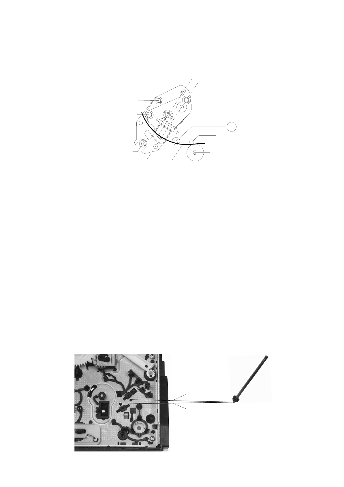
TVR 3710 …, TVR 5100 …, TVR 5500 … Laufwerk / Drive Mechanism
3.1.2 Kombikopf
Einstellen des Neigungswinkels (Tilt)
– Das Laufwerk in eine Feature-Funktion (z.B. Bildsuchlauf 7-fach
vorwärts) bringen.
– Mit der Schraube für den Neigungswinkel (Fig. 25) die Bandunter-
kante gut auf die Bandführung "A1" aufsetzen (das Band darf nicht
an der Unterkante eingerollt sein).
Höhen-Einstellschraube
Height adjustment screw
Azimut-Einstellschraube
Azimuth adjustment screw
Exzenterschraube X
Eccentric screw X
Band
Tape
Einstellung des Azimutwinkels und der Kopfhöhe
– Oszilloskop an den Audioausgang anschließen.
– Testcassette mit dem Standardton-Audiosignal 400Hz wiederge-
ben.
– Mit der Höheneinstellschraube maximale Ausgangsspannung ein-
stellen (Fig. 25).
– Testcassette mit dem Standardton-Audiosignal 8kHz wiedergeben.
– Mit der Azimuteinstellschraube auf maximale Ausgangsspannung
einstellen (Fig. 25).
– Diesen Vorgang gegebenenfalls wiederholen.
– Neigungswinkel kontrollieren.
Wenn der Bandlauf komplett verstellt war oder mehrere Teile des
Bandlaufes getauscht wurden, müssen die Einstellungen der Punkte
3.1.1 und 3.1.2 gegebenenfalls mehrmals durchgeführt werden.
3.2 Einstellung des X-Abstandes
– Vor dieser Einstellung muß die Testcassette erneut eingelegt wer-
den (von Eject-Stellung starten).
– Den Schwarz/Weiß-Teil der Testcassette wiedergeben.
– Taste . drücken.
– "SPURLAGE" mit der Taste | wählen.
– Taste m CL drücken, das Autotracking ist dabei ausgeschaltet.
– Mit der Exzenterschraube (Fig. 25) das Trackingsignal "TRIV" auf
Maximum stellen (DC-gekoppelt).
– Taste "Standby" drücken oder durch Trennen des Gerätes vom
Netz.
3.1.2 A/C (combi) Head
Tilt Angle Adjustment
– Set the tape deck to a feature mode (e.g. picture search forward, 7-
times normal play).
– By means of the tilt adjustment screw (Fig. 25) move the tape until
the lower edge just touches the tape guide "A1" (the lower edge of
the tape must not bend).
Neigungswinkel-Einstellschraube
Tilt adjustment screw
Bandführung
A1
Tape guide
Capstan
Andruckrolle
Pressure roller
Fig. 25
Adjustment of the Azimuth Angle and Height of the Head
– Connect an oscilloscope to the Audio output.
– Play the 400Hz standard audio signal recording on the test tape.
– Adjust for maximum output voltage with the height adjustment screw
(Fig. 25).
– Play the 8kHz standard audio signal recording on the test tape.
– Adjust to maximum output voltage with the azimuth adjustment
screw (Fig. 25).
– If necessary, repeat this process.
– Check the tilt angle.
If the tape transport was completely out of adjustment or if several
components in the tape path have been replaced, the adjustments
described under the paras 3.1.1 and 3.1.2 have to be repeated several
times.
3.2 Adjustment of the Horizontal Distance (x-distance)
– Before this adjustment, take out and reload the test cassette (start
from Eject position).
– Play back the black/white recording on the test cassette.
– Press the . button.
– Select "TRACKING" with the | button.
– Press the m CL button, the Autotracking function is switched off
in this case.
– With the eccentric screw (Fig. 25) adjust the "TRIV" tracking signal
to maximum voltage (DC-coupling).
– Press the "Standby" button or disconnect the mains.
Bandzug-Einstellstift
Bremsbandeinstellung
Brake Band Adjustment
Bandzugeinstellung
Tape Tension Adjustment
Tape tension adjustment pin
Fig. 26
GRUNDIG Service 5 - 11
Page 89
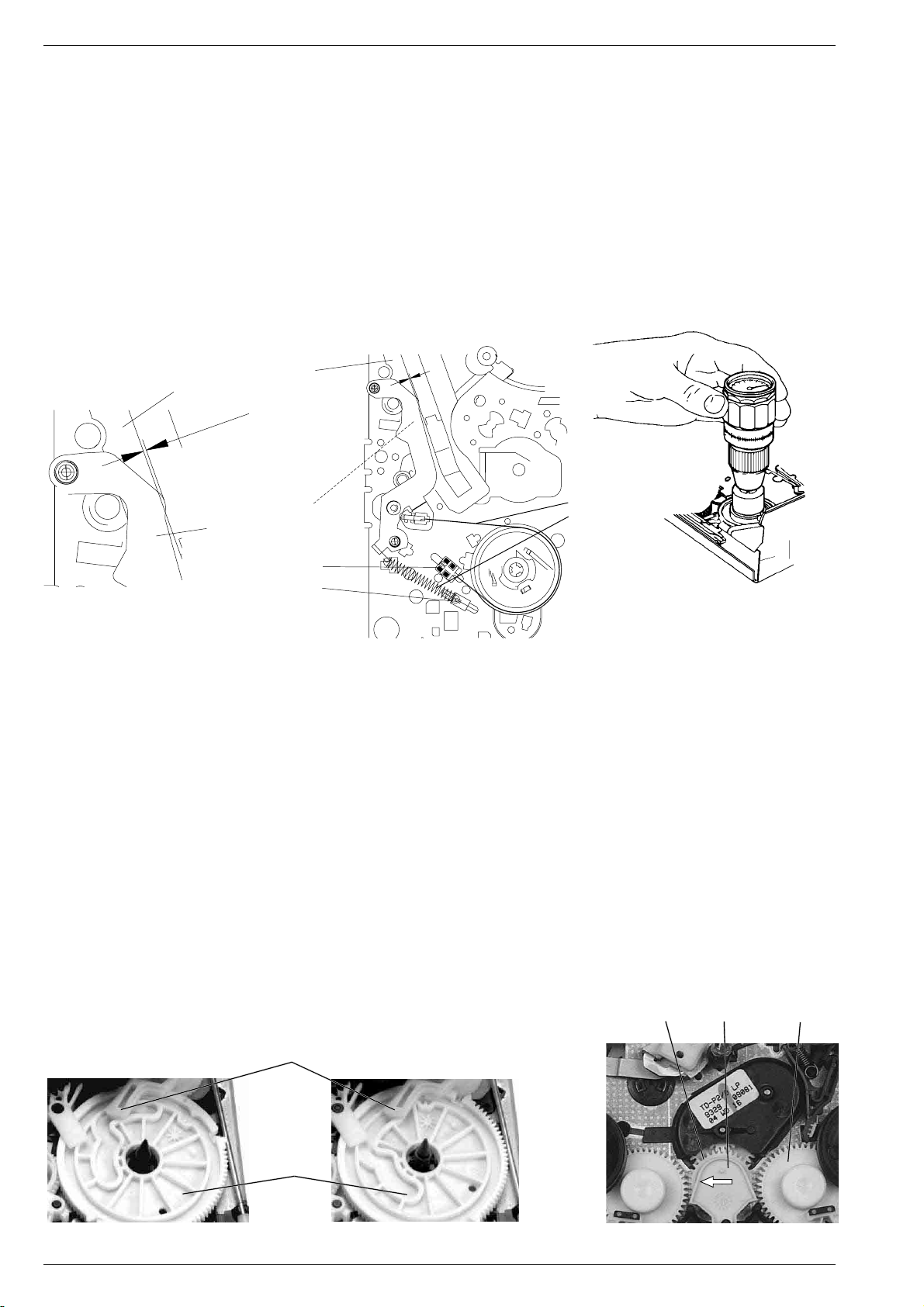
Laufwerk / Drive Mechanism TVR 3710 …, TVR 5100 …, TVR 5500 …
3.3 Bremsbandeinstellung
– Cassettenschacht absenken (Punkt 1.1). Riemenscheibe des Fä-
delmotors (Fig. 3) in Richtung "Einfädeln" drehen, bis das Kurvenrad
in der abgebildeten Stellung (Fig. 29) ist.
– Mittels Bandzug-Einstellwerkzeug (von der Unterseite des Lauf-
werks, Fig. 26) das Bremsband (Fig. 27, Pos. 14P) so einstellen, daß
die Nase des Bandzugfühlers (Pos. 15) deckungsgleich mit der
linken inneren Führungskante der Führung links ist (Fig. 27).
3.4 Bandzugeinstellung
– Eine Cassette (E180) vom Bandanfang ausgehend wiedergeben.
– Mit dem Tentelometer den Bandzug zwischen Hauptlöschkopf
(Fig. 22, Pos. 16) und der Umlenkrolle (Fig. 22, Pos. 23) messen
(dazu den Hauptlöschkopf nach links drücken).
– Mit dem Bandzug-Einstellwerkzeug die Feder (Fig. 27, Pos.11) auf
einen Bandzug von 0,24N ±0,02N (24g ±2g) einstellen (Fig. 27).
linke innere Führungskante
Guiding left
Ø ÷ 0.5mm
Pos. 15
Bandzugfühlhebel
Tension arm
3.3 Brake Band Adjustment
– Lower the cassette compartment (para 1.1). Turn the pulley of the
threading motor (Fig. 3) in the "threading" direction until the cam
wheel takes the position shown in Fig. 29.
– Adjust the brake band (Fig. 27, Pos. 14P) by means of the tape
tension adjustment tool (from the underside of the tape deck, Fig. 26)
so that the edge of the elbow of the tape tension arm (Pos. 15)
overlaps with the left inner edge of the left guide (see Fig. 27).
3.4 Tape Tension Adjustment
– Play a cassette (E 180) starting from the beginning of the tape.
– Measure the tape tension between the full-track erase head (Fig. 22,
Pos. 16) and the reverse roller (Fig. 22, Pos. 23) by means of the
tentelometer (for this press the full-track erase head to the left).
– Adjust the spring (Fig. 27, pos.11) to a tape tension of 0.24N ±0.02N
(24g ±2g) by means of the tape tension adjustment tool (Fig. 27).
Pos. 14P
Pos. 11
Bremsbandjustierung
Brake band adjustment
Bandzugjustierung
Tape tension adjustment
Fig. 27 Fig. 28
3.5 Kontrolle der Rutschkupplung
– Cassettenschacht absenken (Punkt 1.1). Riemenscheibe des Fä-
delmotors (Fig. 3) in Richtung "Einfädeln" drehen, bis das Kurvenrad
in der abgebildeten Stellung (Fig. 29) ist.
– Drehmomentmesser auf den rechten Wickelteller aufsetzen
(Fig. 28).
– Capstanmotor so drehen, daß sich der rechte Wickelteller im
Uhrzeigersinn bewegt.
– So lange drehen, bis sich die Anzeige am Drehmomentmesser nicht
mehr verändert (Fig. 28).
– Drehmoment muß 10,5mNm ±25% (105gf-cm ±25%) sein.
3.6 Kontrolle der Reversebremse
– Cassettenschacht absenken (Punkt 1.1). Riemenscheibe des Fä-
delmotors (Fig. 4) in Richtung "Einfädeln" drehen, bis das Kurvenrad
in der abgebildeten Stellung (Fig. 30) ist.
– Hebel (Fig. 31, Pos. 19R) nach links schwenken, damit das Um-
lenkrad (Pos. 17R) nicht in das rechte Zahnrad (Pos. 18R) eingreift.
– Drehmomentmesser auf den rechten Wickelteller aufsetzen und
entgegen dem Uhrzeigersinn so lange drehen, bis der Wickelteller
leicht durchrutscht (Fig. 28).
– Wert am Drehmomentmesser muß 7mNm ±3mNm (70gf-cm
±30gf-cm) betragen.
3.5 Checking the Friction Clutch
– Lower the cassette compartment (para 1.1). Turn the pulley of the
threading motor (Fig. 3) in the "threading" direction until the cam
wheel takes the position shown in Fig. 29.
– Place the torque meter on the right reel (Fig. 28).
– Turn the capstan motor to move the right reel clockwise.
– Keep turning until the reading on the torque meter does not change
any more (Fig. 28).
– The torquemeter must read 10.5 mNm ±25% (105gf-cm ±25%).
3.6 Checking the Reverse Brake
– Lower the cassette compartment (para 1.1). Turn the pulley of the
threading motor (Fig. 4) in the "threading" direction until the cam
wheel takes the position shown in Fig. 30.
– Turn the lever (Fig. 31, Pos. 19R) to the left so that the swivelling
gear (Pos. 17R) does not engage with the right gearwheel (Pos.
18R).
– Place the torque meter on the right reel and turn the latter counter-
clockwise until the reel just starts to slip (Fig. 28).
– The torquemeter must read 7mNm ±3mNm (70gf-cm ±30gf-cm).
Pos. 17R
Pos. 19R
Pos. 18R
Pos. 41S
Pos. 45S
Fig. 29 Fig. 30
5 - 12 GRUNDIG Service
Fig. 31
Page 90
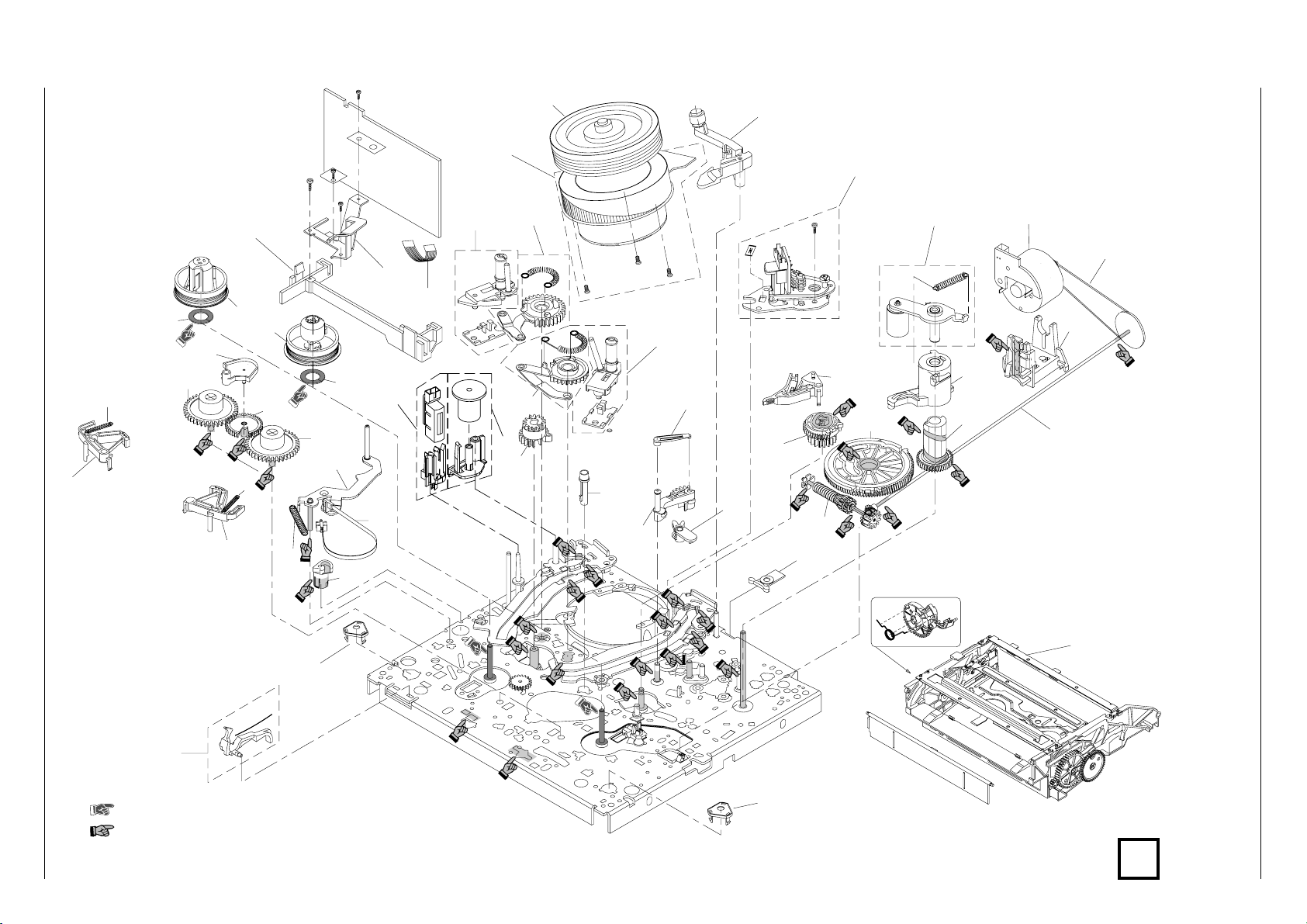
GRUNDIG Service E - 1
Explosionszeichnungen
33
34
35
36
und Ersatzteillisten
TVR 3710 …, TVR 5100 …, TVR 5500 … Explosionszeichnungen und Ersatzteillisten / Exploded Views and Spare Parts Lists
5P
6P
13R
18R
19R
10P
21M
20R
20aR
6P
17R
38
39
40M
47
Exploded Views
and Spare Parts Lists
150
9
27B
25B
24B
28M
31Q
26
42P
30Q
45S
44BS
32Q
48S
49M
23
22M
140
13R
27B
18R
15
14P
11
12
2
37
41S
46S
1
Öl / Oil (Sach-Nr. / Part No. 75988-002.35)
Fett / Grease (Sach-Nr. / Part No. 75988-002.36)
Isopropanol
Fusselfreies Tuch / Fibrefree Tissue
2
1
Page 91
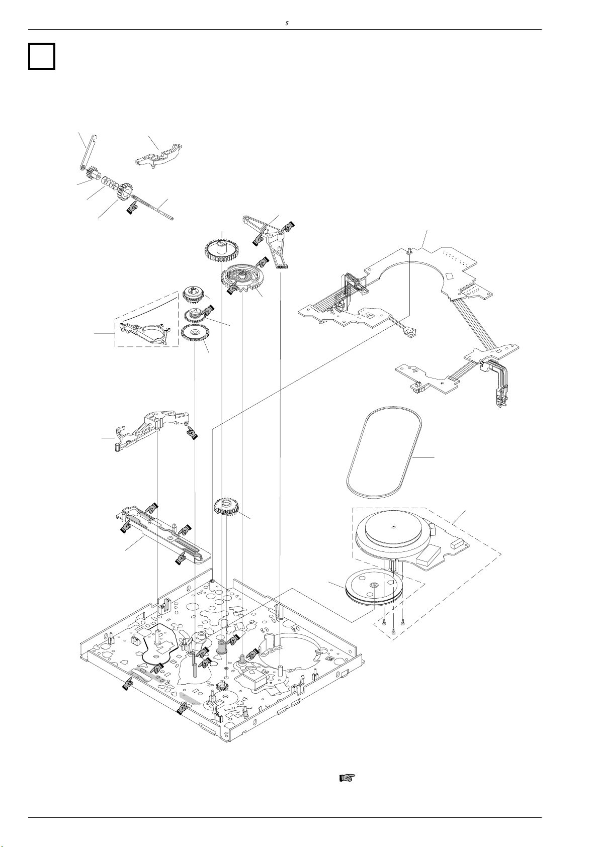
Explosionszeichnungen und Ersatzteillisten / Exploded Views and Spare Parts Lists TVR 3710 …, TVR 5100 …, TVR 5500 …
2
103L
102L
104L
105L
114
101L
106
115
117 I
111B
112M
118
113B
116 I
120M
126
127
129
(Option)
125M
128I
Fett / Grease (Sach-Nr. / Part No. 75988-002.36)
Isopropanol
Fusselfreies Tuch / Fibrefree Tissue
E - 2 GRUNDIG Service
Page 92
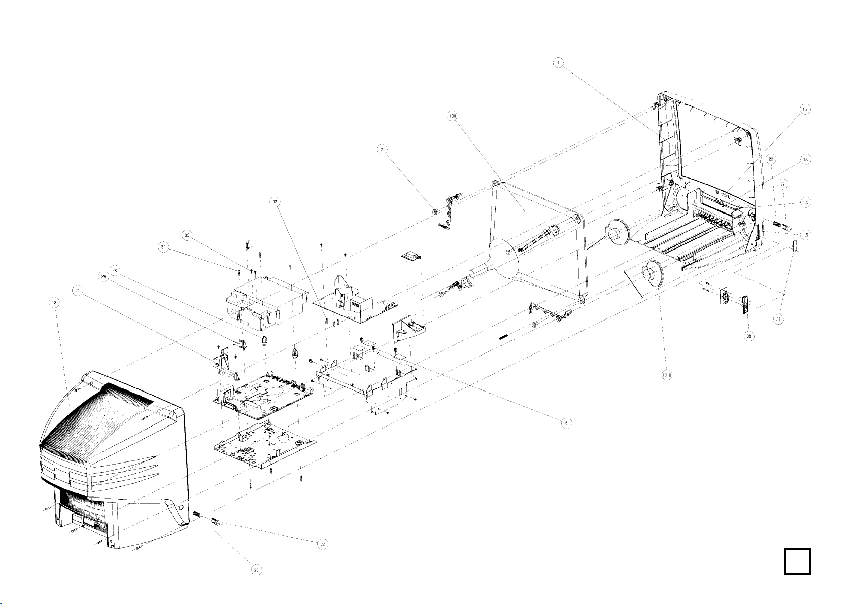
GRUNDIG Service E - 3
TVR 3710 …, TVR 5100 …, TVR 5500 … Explosionszeichnungen und Ersatzteillisten / Exploded Views and Spare Parts Lists
3
Page 93
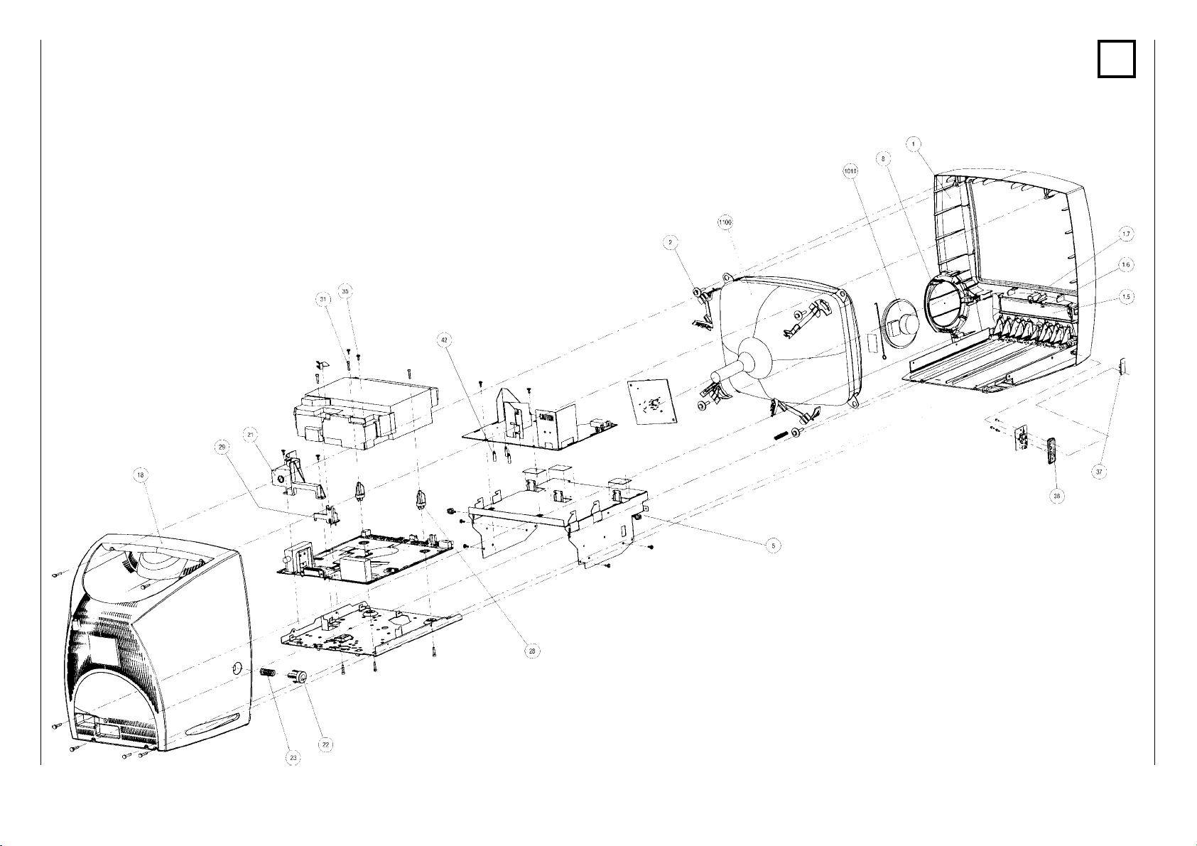
E - 4 GRUNDIG Service
4
Explosionszeichnungen und Ersatzteillisten / Exploded Views and Spare Parts Lists TVR 3710 …, TVR 5100 …, TVR 5500 …
Page 94
GRUNDIG Service E - 5
D
POS. NR.
ABB.
SACHNUMMER ANZ.
POS. NO.
FIG.
PART NUMBER QUA.
BEZEICHNUNG
DESCRIPTION
D
GB
D
POS. NR.
ABB.
SACHNUMMER ANZ.
POS. NO.
FIG.
PART NUMBER QUA.
BEZEICHNUNG
DESCRIPTION
D
GB
TVR 3710 …, TVR 5100 …, TVR 5500 … Explosionszeichnungen und Ersatzteillisten / Exploded Views and Spare Parts Lists
Ersatzteilliste
Spare Parts List
Btx * 32700
4 / 96 TVR 3710
SACH-NR. / PART NO.: 77250-020.75
BESTELL-NR. / ORDER NO.: G.CC 2675
0001.000 4 75988-017.00 GEHAEUSEVORDERTEIL KPL. CABINET FRONT ASSY
0001.500 4 75988-017.01 CASSETTENFACHKLAPPE KPL. LIFT FLAP ASSY
0001.600 4 75988-012.02 SCHENKELFEDER LEG SPRING
0001.700 4 75988-015.01 SCHRIFTZUG LABEL
0002.000 4 75988-015.03 4 SCHRAUBE F. BILDROEHRE SCREW FOR PICTURE TUBE
0005.000 4 75988-015.06 5 KABELKLEMME CABLE CLAMP
0005.100 75988-022.55 ANTENNE ANTENNA
0005.700 75988-017.45 HALTER, FERNBEDIENUNG HOLDER, REMOTE CONTROL
0008.000 4 75988-017.02 2 LAUTSPRECHERGITTER RECHTS KPL. SPEAKER GRILLE RIGHT ASSY
0009.000 75988-017.03 LAUTSPRECHERGITTER LINKS KPL. SPEAKER GRILLE LEFT ASSY
0018.000 4 75988-017.04 RUECKWAND KPL. REAR PANEL ASSY
0021.000 4 75988-022.53 ABDECKUNG KPL. SCART COVER COMPL. SCART
0022.000 4 75988-017.40 KNOPF EIN/AUS KNOB ON/OFF
0023.000 4 75988-017.42 DRUCKFEDER PRESSURE SPRING
0024.000
S
0028.000 4 75988-015.11 2 LAUFWERKHALTER, VORNE TAPE DRIVE HOLDER, FRONT
0029.000 4 75988-015.12 LAUFWERKHALTER, HINTEN TAPE DRIVE HOLDER, REAR
0031.000 4 8114-990-022 6 PLASTITE-SHR 3,5X16 SCREW 3,5X16
0033.000 1 27599-005.08 KOPFRAD 2/0 PAL LP HEAD DISC 2/0 PAL LP
0034.000 1 75988-001.33 SCANNERMOTOR 2/0 SCANNER MOTOR 2/0
0035.000 4 75988-018.18 2 SCHRAUBE, AUDIO SUPPORT SCREW, AUDIO SUPPORT
0037.000 4 75988-025.33 AV-ABDECKUNG AV CAP
0038.000 4 75988-017.87 AV-EINGANG AV INPUT
0040.000
S
0153.000 75988-017.06 FERNBEDIENGEBER TVP762 REMOTE CONTROL TVP762
1010.000 4 75988-017.97 LAUTSPRECHER 8 OHM 3 W LOUDSPEAKER 8OHM 3W
1100.000
5000.000
8001.000 75988-017.09 FLEXIBLE LEITUNG, L3-1901 (7P) FLEXIBLE CABLE, L3-1901 (7P)
8002.000 75988-017.10 FLEXIBLE LEITUNG, L8-1900 (2P) FLEXIBLE CABLE, L8-1900 (2P)
8003.000 75988-012.13 FLEXIBLE LEITUNG, L1-F4 (6P) FLEXIBLE CABLE, L1-F4 (6P)
8004.000 75988-017.47 FLEXIBLE LEITUNG, L4-1903 (3P) FLEXIBLE CABLE, L4-1903 (3P)
8005.000 75988-017.11 FLEXIBLE LEITUNG, L2-1905 (15P) FLEXIBLE CABLE, L2-1905 (15P)
8006.000 75988-017.12 FLEXIBLE LEITUNG, 1941-1902 (10P) FLEXIBLE CABLE, 1941-1902 (10P)
8007.000 75988-017.13 FLEXIBLE LEITUNG, LSP-1914 (2P) FLEXIBLE CABLE, LSP-1914 (2P)
8008.000 75988-017.14 FLEXIBLE LEITUNG, 1913-1967 (5P) FLEXIBLE CABLE, 1913-1967 (5P)
8011.000 75988-017.15 FLEXIBLE LEITUNG, 1912-1923 (7P) FLEXIBLE CABLE, 1912-1923 (7P)
8012.000 75988-017.16 FLEXIBLE LEITUNG, 1911-1922 (5P) FLEXIBLE CABLE, 1911-1922 (5P)
8013.000 75988-017.18 FLEXIBLE LEITUNG, 1909-1921 (13P) FLEXIBLE CABLE, 1909-1921 (13P)
8014.000 75988-324.35 FLEXIBLE LEITUNG, HA-SC FLEXIBLE CABLE, HA-SC
8017.000 75988-017.19 FLEXIBLE LEITUNG, 1971-1935 (3P) FLEXIBLE CABLE, 1971-1935 (3P)
8018.000 75988-017.20 FLEXIBLE LEITUNG, 1918-1937 (4P) FLEXIBLE CABLE, 1918-1937 (4P)
75988-017.86 NETZKABEL 14"PAL+/59 POWER CABLE 14"PAL+/59
S
27599-004.07 KOPFVERSTAERKER OHA 2/0 HEAD AMPLIFIER OHA 2/0
75988-025.01 X HSD-LW WDBT 2/0 HSD TAPE DRIVE WDBT 2/0
S
75988-018.50 X LEISTUNGS-CHASSIS PLSP14B POWER CHASSIS PLSP14B
S
75988-018.70 X SIGNALCHASSIS PSSPG1/GVXF SIGNAL CHASSIS PSSPG1/GVXF
S4 75988-017.07 BILDROEHRE A34 JLL 90X74W CRT A34 JLL 90X74W
S
75988-017.08 ENTMAGNETISIERUNGSSPULE DEGAUSSING COIL
72010-524.75 BEDIENUNGSANLEITUNG D/I/E/P INSTRUCTION MANUALE D/I/E/P
72010-524.95 SERVICE MANUAL D/GB SERVICE MANUAL D/GB
KEIN E-TEIL NO SPARE PART
(LEISTUNGS-CHASSIS, BILDROHRPLATTE, (POWER CHSSIS, PICTURE TUBE BOARD,
BUCHSENPLATTE) SOCKET BOARD)
KEIN E-TEIL NO SPARE PART
KEIN E-TEIL NO SPARE PART
X = SIEHE GESONDERTE E-LISTE X = SEE SEPARATE PARTS LIST
Ersatzteilliste
Spare Parts List
#
Btx * 32700
#
4 / 96 TVR 3710 GB
SACH-NR. / PART NO.: 77250-023.75
BESTELL-NR. / ORDER NO.: G.CC 2875 GB
0001.000 4 75988-017.00 GEHAEUSEVORDERTEIL CABINET FRONT
0001.500 4 75988-017.01 CASSETTENFACHKLAPPE CASS.COMP.LID
0001.600 4 75988-000.08 SCHENKELFEDER LEG SPRING
0001.700 4 75988-015.01 SCHRIFTZUG WORDMARK
0002.000 4 75988-015.03 4 SCHRAUBE F. BILDROEHRE SCREW FOR PICTURE TUBE
0005.000 4 75988-015.06 5 KABELKLEMME CABLE CLAMP
0005.100 75988-022.55 ANTENNE ANTENNA
0005.700 75988-017.45 HALTER, FERNBEDIENUNG HOLDER, REMOTE CONTROL
0008.000 4 75988-017.02 LAUTSPRECHERGITTER RE KPL. SPEAKER GRILLE RH CPL.
0009.000 75988-017.03 LAUTSPRECHERGITTER LI KPL. SPEAKER GRILLE LEFT CPL.
0018.000 4 75988-017.04 RUECKWAND KPL. REAR PANEL CPL.
0021.000 4 75988-022.53 ABDECKUNG KPL. SCART COVER COMPL.
0022.000 4 75988-017.40 KNOPF EIN/AUS KNOB ON/OFF
0023.000 4 75988-017.42 DRUCKFEDER PRESSURE SPRING
0024.000
S
0028.000 4 75988-015.11 2 LAUFWERKHALTER, VORNE TAPE DRIVE HOLDER, FRONT
0029.000 4 75988-015.12 LAUFWERKHALTER, HINTEN TAPE DRIVE HOLDER, REAR
0031.000 4 8114-990-022 6 PLASTITE SHR 3,5X16 SCREW 3,5X16
0033.000 1 27599-005.07 KOPFRAD 2/0 LP PAL HEAD DISC 3,5X16
0034.000 1 75988-001.33 SCANNERMOTOR 2/0 SCANNER MOTOR 2/0
0035.000 4 75988-018.18 2 SCHRAUBE, AUDIO SUPPORT SCREW, AUDIO SUPPORT
0037.000 4 75988-025.33 AV-ABDECKUNG AV-CAP
0038.000 4 75988-017.87 AV-EINGANG AV INPUT
0040.000
0153.000 75988-017.06 FERNBEDIENGEBER TVP762 REMOTE CONTROL TVP 762
1010.000 4 75988-017.97 LAUTSPRECHER 8 OHM 3 W SPEAKER 8OHM 3W
1100.000
5000.000
8001.000 75988-017.09 FLEXIBLE LEITUNG, L3-1901 (7P) FLEXIBLE CABLE, L3-1901 (7P)
8002.000 75988-026.07 FLEXIBLE LEITUNG, L8-1900 (2P) FLEXIBLE CABLE, L8-1900 (2P)
8003.000 75988-003.20 FLEXIBLE LEITUNG, L1-F4 (6P) FLEXIBLE CABLE, L1-F4 (6P)
8004.000 75988-017.47 FLEXIBLE LEITUNG, L4-1903 (3P) FLEXIBLE CABLE, L4-1903 (3P)
8005.000 75988-017.11 FLEXIBLE LEITUNG, L2-1905 (15P) FLEXIBLE CABLE, L2-1905 (15P)
8006.000 75988-017.12 FLEXIBLE LEITUNG, 1941-1902 (10P) FLEXIBLE CABLE, 1941-1902 (10P)
8007.000 75988-017.13 FLEXIBLE LEITUNG, LSP-1914 (2P) FLEXIBLE CABLE, LSP-1914 (2P)
8008.000 75988-017.14 FLEXIBLE LEITUNG, 1913-1967 (5P) FLEXIBLE CABLE, 1913-1967 (5P)
8011.000 75988-026.14 FLEXIBLE LEITUNG, 1912-1923 (7P) FLEXIBLE CABLE, 1912-1923 (7P)
8012.000 75988-017.16 FLEXIBLE LEITUNG, 1911-1922 (5P) FLEXIBLE CABLE, 1911-1922 (5P)
8013.000 75988-017.18 FLEXIBLE LEITUNG, 1909-1921(13P) FLEXIBLE CABLE, 1909-1921 (13P)
8014.000 75988-324.35 FLEXIBLE LEITUNG, HA-SC FLEXIBLE CABLE, HA-SC
8017.000 75988-017.19 FLEXIBLE LEITUNG, 1971-1935 (3P) FLEXIBLE CABLE, 1971-1935 (3P)
8018.000 75988-017.20 FLEXIBLE LEITUNG, 1918-1937 (4P) FLEXIBLE CABLE, 1918-1937 (4P)
75988-019.02 NETZKABEL 14" GB/05 POWER CABLE 14" GB/05
S
27599-004.08 KOPFVERSTAERKER OHA 2/0 LP HEAD AMPLIFIER OHA 2/0 LP
S
75988-025.00 X ECO-LW WDB 2/0 L/P ECO TAPE DRIVE WDB 2/0
S
75988-018.50 X LEISTUNGS-CHASSIS PLSP14B POWER CHASSIS PLSP14B
S
75988-018.78 X SIGNALCHASSIS PSSPG1/ILPPVXT SIGNAL CHASSIS PSSPG1/ILPPVXT
S4 75988-017.07 BILDROEHRE A34 JLL 90X74W PICTURE TUBE A34JLL90X74W
S
75988-017.08 ENTMAGNETISIERUNGSSPULE DEGAUSSING COIL
72010-524.76 BEDIENUNGSANLEITUNG GB INSTRUCTION MANUAL GB
72010-524.95 SERVICE MANUAL D/GB SERVICE MANUAL D/GB
KEIN E-TEIL NO SPARE PART
(LEISTUNGS-CHASSIS, BILDROHRPLATTE, (POWER CHSSIS, PICTURE TUBE BOARD,
BUCHSENPLATTE) SOCKET BOARD)
KEIN E-TEIL NO SPARE PART
KEIN E-TEIL NO SPARE PART
X = SIEHE GESONDERTE E-LISTE X = SEE SEPARATE PARTS LIST
Page 95
E - 6 GRUNDIG Service
D
POS. NR.
ABB.
SACHNUMMER ANZ.
POS. NO.
FIG.
PART NUMBER QUA.
BEZEICHNUNG
DESCRIPTION
D
GB
D
POS. NR.
ABB.
SACHNUMMER ANZ.
POS. NO.
FIG.
PART NUMBER QUA.
BEZEICHNUNG
DESCRIPTION
D
GB
Explosionszeichnungen und Ersatzteillisten / Exploded Views and Spare Parts Lists TVR 3710 …, TVR 5100 …, TVR 5500 …
Ersatzteilliste
Spare Parts List
Btx
32700
*
4 / 96 TVR 5100
SACH-NR. / PART NO.: 77250-030.75 BESTELL-NR. / ORDER NO.:G.CC 3075
SACH-NR. / PART NO.: 77250-031.75 BESTELL-NR. / ORDER NO.:G.CC 3175 *
SACH-NR. / PART NO.: 77250-032.75 BESTELL-NR. / ORDER NO.:G.CC 3275 **
0001.000 3 75988-019.05 GEHAEUSEVORDERTEIL CABINET FRONT
0001.500 3 75988-019.06 CASSETTENFACHKLAPPE LIFT FLAP ASSZ
0001.600 3 75988-000.08 SCHENKELFEDER LEG SPRING
0001.700 3 75988-026.02 SCHRIFTZUG LABEL
0001.900 3 75988-026.03 ABDECKUNG VORNE COVER, FRONT
0002.000 3 75988-026.04 4 SCHRAUBE, BILDROEHRE SCREW FOR PICTURE TUBE
0005.000 3 75988-015.06 4 KABELKLEMME CABLE CLAMP
0018.000 3 75988-026.05 RUECKWAND KPL. REAR PANEL ASSY
0021.000 75988-022.53 ABDECKUNG KPL. SCART COVER CPL. SCART
0022.000 3 75988-026.06 KNOPF AUS/EIN KNOB ON/OFF
0023.000 3 75988-017.42 DRUCKFEDER PRESSURESPRING
0024.000
S 75988-026.12 NETZKABEL 20"/21" PAL POWER CABLE 20"/21" PAL
0028.000 3 75988-015.11 2 LAUFWERKHALTER, VORNE TAPE DRIVE BRACKET, FRONT
0029.000 3 75988-015.12 LAUFWERKHALTER, HINTEN TAPE DRIVE BRACKET, REAR
0031.000 3 8114-990-022 6 PLASTITE SHR 3,5X16 SCREW 3,5X16
0033.000 1 27599-005.07 KOPFRAD 2/0 PAL HEAD DISC 2/0 PAL
0034.000 1 75988-001.33 SCANNERMOTOR 2/0 SCANNER MOTOR 2/0
0035.000 3 75988-018.18 2 SCHRAUBE, AUDIO SUPPORT SCREW, AUDIO SUPPORT
0038.000 3 75988-019.08 AV-EINGANG AV INPUT
0040.000
S 27599-004.07 KOPFVERSTAERKER OHA 2/0 HEAD AMPLIFIER OHA 2/0
S 75988-025.00 X ECO-LW WDB 2/0 ECO TAPE DRIVE WDB 2/0
S 75988-018.52 X LEISTUNGS-CHASSIS PLSP20BK POWER CHASSIS PLSP20BK
S 75988-018.75 X SIGNALCHASSIS PSSPG1/GVX SIGNAL CHASSIS PSSPG1/GVX
S 75988-018.71 X SIGNALCHASSIS PSSPG1/GPVX * SIGNAL CHASSIS PSSPG1/GPVX *
S 75988-018.72 X SIGNALCHASSIS PSSPG2/GPVX ** SIGNAL CHASSIS PSSPG2/GPVX **
0153.000 75988-017.06 FERNBEDIENGEBER TVP762 REMOTE CONTROL TVP 762
1000.000
S3 75988-019.10 BILDROEHRE A48ECR31X60 PICTURE TUBE A48ECR31X60
1010.000 3 75988-017.97 LAUTSPRECHER 8 OHM 3 W SPEAKER 8OHM 3W
5000.000
S 75988-026.11 ENTMAGNETISIERUNGSPULE 435 DEGAUSSING COIL 435
8001.000 75988-017.09 FLEXIBLE LEITUNG, L3-1901 (7P) FLEXIBLE CABLE, L3-1901 (7P)
8002.000 75988-017.10 FLEXIBLE LEITUNG, L8-1900 (2P) FLEXIBLE CABLE, L8-1900 (2P)
8003.000 75988-012.13 FLEXIBLE LEITUNG, L1-F4 (6P) FLEXIBLE CABLE, L1-F4 (6P)
8004.000 75988-017.47 FLEXIBLE LEITUNG, L4-1903 (3P) FLEXIBLE CABLE, L4-1903 (3P)
8005.000 75988-017.11 FLEXIBLE LEITUNG, L2-1905 (15P) FLEXIBLE CABLE, L2-1905 (15P)
8006.000 75988-017.12 FLEXIBLE LEITUNG,1941-1902 (10P) FLEXIBLE CABLE, 1941-1902 (10P)
8007.000 75988-017.13 FLEXIBLE LEITUNG, LSP-1914 (2P) FLEXIBLE CABLE, LSP-1914 (2P)
8008.000 75988-017.14 FLEXIBLE LEITUNG,1913-1967 (5P) FLEXIBLE CABLE, 1913-1967 (5P)
8011.000 75988-026.14 FLEXIBLE LEITUNG, 1912-1923 (7P) FLEXIBLE CABLE, 1912-1923 (7P)
8012.000 75988-017.16 FLEXIBLE LEITUNG, 1911-1922 (5P) FLEXIBLE CABLE, 1911-1922 (5P)
8013.000 75988-017.18 FLEXIBLE LEITUNG, 1909-1921(13P) FLEXIBLE CABLE, 1909-1921 (13P)
8014.000 75988-324.35 FLEXIBLE LEITUNG, HA-SC FLEXIBLE CABLE, HA-SC
8017.000 75988-017.19 FLEXIBLE LEITUNG, 1971-1935 (3P) FLEXIBLE CABLE, 1971-1935 (3P)
72010-524.80 BEDIENUNGSANLEITUNG D/I/E/P OPERATING INSTRUCTIONS D/I/E/P
72010-524.81 BEDIENUNGSANLEITUNG NL/F * OPERATING INSTRUCTIONS NL/F *
72010-524.82 BEDIENUNGSANLEITUNG S/N/DK/SF ** OPERATING INSTRUCTIONS S/N/DK/SF **
72010-524.95 SERVICE MANUAL D/GB SERVICE MANUAL D/GB
KEIN E-TEIL NO SPARE PART
(LEISTUNGS-CHASSIS, BILDROHRPLATTE, (POWER CHSSIS, PICTURE TUBE BOARD,
NETZSCHALTERPLATTE, BUCHSENPLATTE) POWER SUPPLY BOARD, SOCKET BOARD)
KEIN E-TEIL NO SPARE PART
KEIN E-TEIL NO SPAREPART
KEIN E-TEIL NO SPAREPART
KEIN E-TEIL NO SPAREPART
X = SIEHE GESONDERTE E-LISTE X = SEE SEPARATE PARTS LIST
Ersatzteilliste
Spare Parts List
#
Btx
32700
*
#
4 / 96 TVR 5500
SACH-NR. / PART NO.: 77250-040.75
BESTELL-NR. / ORDER NO.: G.CC 3475
0001.000 3 75988-019.07 GEHAEUSEVORDERTEIL KPL. CABINET FRONT ASSY
0001.500 3 75988-019.06 CASSETTENFACHKLAPPE LIFT FLAP ASSY
0001.600 3 75988-000.08 SCHENKELFEDER LEG SPRING
0001.700 3 75988-026.02 SCHRIFTZUG LABEL
0001.900 3 75988-026.03 ABDECKUNG VORNE COVER - FRONT
0002.000 3 75988-026.04 4 SCHRAUBE, BILDROEHRE SCREW PICTURE TUBE
0005.000 3 75988-015.06 4 KABELKLEMME CABLE CLAMP
0018.000 3 75988-026.05 RUECKWAND KPL. REAR PANEL CPL.
0021.000 3 75988-022.53 ABDECKUNG KPL. SCART COVER COMPL. SCART
0022.000 3 75988-026.06 KNOPF AUS/EIN KNOB ON /OFF
0023.000 3 75988-017.42 DRUCKFEDER PRESSURESPRING
0024.000
S 75988-026.12 NETZKABEL 20"/21" PAL POWER CABLE 20/21"PAL
0028.000 3 75988-015.11 2 LAUFWERKHALTER, VORNE TAPE DRIVE BRACKET, REAR
0029.000 3 75988-015.12 LAUFWERKHALTER, HINTEN TAPE DRIVE BRACKET, FRONT
0031.000 3 8114-990-022 6 PLASTITE SHR 3,5X16 SCREW 3,5X16
0033.000 1 27599-005.08 KOPFRAD 2/0 PAL HEAD DISC 2/0 PAL
0034.000 1 75988-001.33 SCANNERMOTOR 2/0 SCANNER MOTOR 2/0
0035.000 3 75988-018.18 2 SCHRAUBE, AUDIO SUPPORT SCREW, AUDIO SUPPORT
0037.000 3 75988-026.08 AV-ABDECKUNG AV COVER
0038.000 3 75988-025.07 AV-EINGANG AV INPUT
0040.000
S 27599-004.07 KOPFVERSTAERKER OHA 2/0 HEAD AMPLIFIER OHA 2/0
S 75988-025.01 X HSD-LW WDBT 2/0 HSD TAPE DRIVE WDBT 2/0
S 75988-018.51 X LEISTUNGS-CHASSIS PLSP21B POWER CHASSIS PLSP21B
S 75988-018.76 X SIGNALCHASSIS PSSPG1/GVXTF SIGNAL CHASSIS PSSPG1/GVXTF
0153.000 75988-017.06 FERNBEDIENGEBER TVP762 REMOTE CONTROL TVP 762
1010.000 3 75988-025.09 2 LAUTSPRECHER RND 102 16R LOUDSPEAKER RND 102 16R
1100.000
S3 75988-026.10 BILDROEHRE A51EAL165X00 PICTURE TUBE A51EAL165X00
5000.000
S 75988-019.11 ENTMAGNETISIERUNGSSPULE 435 DEGAUSSING COIL 435
8001.000 75988-017.09 FLEXIBLE LEITUNG, L3-1901 (7P) FLEXIBLE CABLE, L3-1901 (7P)
8002.000 75988-026.07 FLEXIBLE LEITUNG, L8-1900 (2P) FLEXIBLE CABLE, L8-1900 (2P)
8003.000 75988-012.13 FLEXIBLE LEITUNG, L1-F4 (6P) FLEXIBLE CABLE, L1-F4 (6P)
8004.000 75988-017.47 FLEXIBLE LEITUNG, L4-1903 (3P) FLEXIBLE CABLE, L4-1903 (3P)
8005.000 75988-017.11 FLEXIBLE LEITUNG, L2-1905 (15P) FLEXIBLE CABLE, L2-1905 (15P)
8006.000 75988-017.12 FLEXIBLE LEITUNG, 1941-1902 (10P) FLEXIBLE CABLE, 1941-1902 (10P)
8007.000 75988-017.13 FLEXIBLE LEITUNG, LSP-1914 (2P) FLEXIBLE CABLE, LSP-1914 (2P)
8008.000 75988-017.14 FLEXIBLE LEITUNG, 1913-1967 (5P) FLEXIBLE CABLE, 1913-1967 (5P)
8011.000 75988-026.14 FLEXIBLE LEITUNG, 1912-1923 (7P) FLEXIBLE CABLE, 1912-1923 (7P)
8012.000 75988-017.16 FLEXIBLE LEITUNG, 1911-1922 (5P) FLEXIBLE CABLE, 1911-1922 (5P)
8013.000 75988-017.18 FLEXIBLE LEITUNG, 1909-1921 (13P) FLEXIBLE CABLE, 1909-1921 (13P)
8014.000 75988-324.35 FLEXIBLE LEITUNG, HA-SC FLEXIBLE CABLE, HA-SC
8015.000 75988-026.15 FLEXIBLE LEITUNG, LSP-1970 (2P) FLEXIBLE CABLE, LSP-1970 (2P)
8017.000 75988-017.19 FLEXIBLE LEITUNG, 1971-1935 (3P) FLEXIBLE CABLE, 1971-1935 (3P)
8018.000 75988-017.20 FLEXIBLE LEITUNG, 1918-1937 (4P) FLEXIBLE CABLE, 1918-1937 (4P)
72010-524.85 BEDIENUNGSANLTG.D/I/E/P INSTRUCTION MANUAL
72010-524.95 SERVICE MANUAL D/GB SERVICE MANUAL D/GB
KEIN E-TEIL NO SPARE PART
(LEISTUNGS-CHASSIS, BILDROHRPLATTE, (POWER CHSSIS, PICTURE TUBE BOARD,
NETZSCHALTERPLATTE, BUCHSENPLATTE) POWER SUPPLY BOARD, SOCKET BOARD)
KEIN E-TEIL NO SPARE PART
KEIN E-TEIL NO SPARE PART
X = SIEHE GESONDERTE E-LISTE X = SEE SEPARATE PARTS LIST
Page 96
GRUNDIG Service E - 7
D
POS. NR.
ABB.
SACHNUMMER ANZ.
POS. NO.
FIG.
PART NUMBER QUA.
BEZEICHNUNG
DESCRIPTION
D
GB
BEZEICHNUNG
DESCRIPTION
SACHNUMMER
PART NUMBER
POS. NR.
POS. NO.
BEZEICHNUNG
DESCRIPTION
SACHNUMMER
PART NUMBER
POS. NR.
POS. NO.
BEZEICHNUNG
DESCRIPTION
SACHNUMMER
PART NUMBER
POS. NR.
POS. NO.
BEZEICHNUNG
DESCRIPTION
SACHNUMMER
PART NUMBER
POS. NR.
POS. NO.
Ersatzteilliste
Spare Parts List
4 / 96
0009.000 S 75988-010.55 SICHERUNGSHALTER FUSE HOLDER
0067.000
S 75988-017.49 FLEX.LEITUNG1926-1969(4P) FLEX. CABLE 1926-1969(4P)
1000.000
S 75988-015.19 NETZSCHALTER POWER SWITCH
1300.000
S 75988-021.31 FUNKENSTRECKE SPARK GAP
1926.000 75988-021.35 STECKVERB. 4P DIPMATE CON 4P DIPMATE
1931.000 75988-021.36 STECKVERB. 5P HSJ 1406 CON 5P HSJ 1406
1933.000 75988-021.37 STECKVERB. DOPPEL CIN 4P CON DOUBLE CIN 4P
1961.000
S 75988-021.32 SOCKEL BILDROEHRE 4454-S CRT SOCKET 4454-S
1962.000
S 75988-021.33 FLEX.LEITUNG AQUADAC 14" FLEX. CABLE AQUADAC 14"
LEISTUNGS-CHASSIS PLSP14B
(LEISTUNGS-CHASSIS, BILDROHRPLATTE, BUCHSENPLATTE)
POWER CHASSIS PLSP14B
(POWER CHASSIS, PICTURE TUBE BOARD, SOCKET BOARD)
SACH-NR. / PART NO.: 75988-018.50
Btx * 32700
TVR 3710 …, TVR 5100 …, TVR 5500 … Explosionszeichnungen und Ersatzteillisten / Exploded Views and Spare Parts Lists
L 5350 75988-017.23 DROSSEL/CHOKE COIL
#
L 5351 75988-017.23 DROSSEL/CHOKE COIL
L 5352 75988-017.28 SPULE 22UH/COIL
L 5353 75988-010.52 SPULE 22UH/COIL
L 5354 75988-017.23 DROSSEL/CHOKE COIL
L 5363 75988-017.23 DROSSEL/CHOKE COIL
L 5364 75988-017.23 DROSSEL/CHOKE COIL
L 5365 75988-017.23 DROSSEL/CHOKE COIL
L 5366 75988-010.52 SPULE 22UH/COIL
L 5370 75988-017.23 DROSSEL/CHOKE COIL
L 5371 75988-010.52 SPULE 22UH/COIL
L 5372 75988-010.52 SPULE 22UH/COIL
L 5373 75988-010.52 SPULE 22UH/COIL
L 5374 75988-017.28 SPULE 22UH/COIL
L 5556 75988-010.52 SPULE 22UH/COIL
L 5590 8140-526-326 DR AX 0411-GA 47UH
L 5901 75988-021.19 SPULE 10U PM5 SPT0508/COIL
L 5902 8140-526-412 DR AX 0411 10UH
R 3300
S 75988-019.20 WIDERST. VR37 4,7 MOHM
R 3309
S 75988-027.62 WIDERST. VARIABEL
R 3310
S 75988-017.93 PTC-WIDERST. 2K 265 VS
R 3312
S 75988-001.77 WIDERST.3,9MOHM
R 3313
S 75988-001.77 WIDERST.3,9MOHM/
R 3338
S 75988-019.21 MSW 0207 39 OHM 5% AX.
R 3358 75988-033.04 CERM TRIM 4,7KOHM PM25
R 3523 8792-001-309 ESTR.P6/A 100 OHM LIN
R 3524 8792-001-146 ESTR.P6/A 4,7 KOHM LIN
R 3531 75952-030.91 MSW NB 0207 4,7 OHM 5% GA
R 3532 75951-701.18 MSW NB 0207 4,7 OHM 5% AX
R 3537 75951-701.18 MSW NB 0207 4,7 OHM 5% AX
R 3592 75952-030.91 MSW NB 0207 4,7 OHM 5% GA
RESISTOR
C 2311 S
C 2312
C 2315
C 2328
C 2335
C 2352
C 2363
C 2373
C 2374
C 2379
C 2512
C 2519
C 2584
C 2585
C 2586
C 2589
C 2592
C 2593
D 6272 75987-392.37 DIODE BZX 79 C 6 V 8
D 6273 75987-392.37 DIODE BZX 79 C 6 V 8
D 6274 75987-392.37 DIODE BZX 79 C 6 V 8
D 6275 75987-392.37 DIODE BZX 79 C 6 V 8
D 6313 75988-027.75 DIODE 1 N 5062-TAP
D 6314 75988-027.75 DIODE 1 N 5062-TAP
D 6315 75988-027.75 DIODE 1 N 5062-TAP
D 6316 75988-027.75 DIODE 1 N 5062-TAP
D 6332 8309-516-854 DIODE BYT 54 M
D 6334 75987-538.95 DIODE BYD 33 D
D 6335 8309-200-021 DIODE BAV21 ITT/ TFK
D 6336 8309-516-854 DIODE BYT 54 M
D 6337 8309-516-854 DIODE BYT 54 M
75988-017.95 KONDENS.0,47 UF 250V PM20
S
75988-021.34 KONDENS.1NF 250V PM20
S
75988-017.88 ELKO 68UF 385V PM20
S
75988-017.89 KONDENSATOR 220P 1KV PM20
S
75988-019.13 KONDENSATOR 100U 25V PM20/
S
75988-005.91 ELKO 25V 680UF
S
75988-019.14 ELKO 47U 200V PM 20
S
75988-005.91 ELKO 25V 680UF
S
75988-005.91 ELKO 25V 680UF
S
75988-019.15 ELKO 560U 25V PM20 HFQ
S
75988-019.15 ELKO 560U 25V PM20 HFQ
S
75988-019.17 ELKO 1000U 35V PM 20 VR
S
75988-017.90 KONDENSATOR 560N 250V PM5
S
75988-017.91 KONDENSATOR 8,2N 1,6KV PM5
S
75988-017.94 KONDENSATOR 1,2N 2KV PM10
S
75988-017.92 KONDENSATOR 10N 400V PM10/
S
75988-019.18 ELKO 4,7U 250V PM20 VR
S
75988-019.14 ELKO 47U 200V PM 20
CAPACITOR
CAPACITOR
CAPACITOR
ELECTROLYTIC CAPACITOR
D 6348 75988-027.76 DIODE BYV10-20
D 6351 75988-324.25 DIODE BYW 98-200 RL
D 6361 75988-017.32 DIODE BYW 36
D 6371 75988-324.25 DIODE BYW 98-200 RL
D 6372 75988-324.25 DIODE BYW 98-200 RL
D 6373 75988-027.76 DIODE BYV10-20
D 6374 8309-516-854 DIODE BYT 54 M
D 6392 8309-200-021 DIODE BAV21 ITT/ TFK
D 6393 8309-721-034 Z DIODE 6,8 C 1,3W
D 6511 75987-538.95 DIODE BYD 33 D
D 6513 8309-200-021 DIODE BAV21 ITT/ TFK
D 6525 8309-200-021 DIODE BAV21 ITT/ TFK
D 6550 8309-200-021 DIODE BAV21 ITT/ TFK
D 6551 8309-200-021 DIODE BAV21 ITT/ TFK
D 6552 75988-009.83 DIODE BZX 79 C 18
D 6553 8309-200-021 DIODE BAV21 ITT/ TFK
D 6554 75954-012.17 Z DIODE BXZ 79 C24
D 6555 8309-720-330 Z DIODE 30 B 0,5W
D 6556 8309-200-021 DIODE BAV21 ITT/ TFK
D 6581 8309-200-021 DIODE BAV21 ITT/ TFK
D 6582 75987-538.95 DIODE BYD 33 D
D 6583 8309-200-021 DIODE BAV21 ITT/ TFK
D 6584 8309-720-100 Z DIODE 10 C 0,5W
D 6592 8309-204-268 DIODE BYV 16 TFK/BYV 96E/
D 6906 8309-200-021 DIODE BAV21 ITT/ TFK
F 5311
S
75988-021.15 FILTER LINE 30MH DMF-2830
IC 7310 75988-027.79 IC MC 44603 F
IC 7331 75988-000.62 IC TL 431 CLPRP
IC 7350 8305-204-319 IC LM 317 T NSC/SGS
IC 7510 75988-021.21 IC TDA 3653C/N2
IC 7900 75988-021.23 IC TDA 6103Q/N2
SI 1311
S 8315-621-503 SI 5X20 T2,5 A H 250V
SI 1371
S 75988-015.23 SICHERUNG T 2,5 A IEC
SI 1372
S 75988-025.36 SICHERUNG T 2,5 AICE 250V/
T 7330 75988-021.31 TRANS. FET STP NA60FI
T 7351 8303-205-548 TRANS. BC548B
T 7352 75988-021.20 TRANS. FET POW MTP3055E
T 7550 8303-205-548 TRANS. BC548B
T 7578 8303-205-558 TRANS. BC558B
T 7583 75988-021.22 TRANS. BU 1508DX
T 7584 8302-420-044 TRANS. MPS-A 43 MOT WW.
T 7585 8303-205-548 TRANS. BC548B
T 7587 8303-205-548 TRANS. BC548B
T 7901 8303-205-548 TRANS. BC548B
T 7902 8303-205-548 TRANS. BC548B
TR 5331
S 75988-021.16 TRAFO CE 364 14"/
TR 5550 S 75988-021.17 ZEILENTRAFO TR 1142.5046/
TR 5580
S 75988-021.18 TREIBERTRAFO CU 10/
FUSE
TRANSFORMER
LINE TRANSFORMER
DRIVE TRANSFORMER
Es gelten die Vorschriften und Sicherheitshinweise gemäß dem Service Manual "Sicherheit",
Sach-Nummer 72010-800.00, sowie zusätzlich
die eventuell abweichenden, landesspezifischen
Vorschriften!
( )
The regulations and safety instructions shall be
valid as provided by the "Safety" Service Manual,
part number 72010-800.00, as well as the
respective national deviations.
Page 97
E - 8 GRUNDIG Service
D
BEZEICHNUNG
DESCRIPTION
SACHNUMMER
PART NUMBER
POS. NR.
POS. NO.
BEZEICHNUNG
DESCRIPTION
SACHNUMMER
PART NUMBER
POS. NR.
POS. NO.
POS. NR.
ABB.
SACHNUMMER ANZ.
POS. NO.
FIG.
PART NUMBER QUA.
BEZEICHNUNG
DESCRIPTION
D
GB
D
BEZEICHNUNG
DESCRIPTION
SACHNUMMER
PART NUMBER
POS. NR.
POS. NO.
BEZEICHNUNG
DESCRIPTION
SACHNUMMER
PART NUMBER
POS. NR.
POS. NO.
POS. NR.
ABB.
SACHNUMMER ANZ.
POS. NO.
FIG.
PART NUMBER QUA.
BEZEICHNUNG
DESCRIPTION
D
GB
Ersatzteilliste
Spare Parts List
Explosionszeichnungen und Ersatzteillisten / Exploded Views and Spare Parts Lists TVR 3710 …, TVR 5100 …, TVR 5500 …
Ersatzteilliste
Spare Parts List
Btx
32700
*
4 / 96
ALLE NICHT AUFGEFÜHRTEN E-TEILE
SIEHE E-LISTE LEISTUNGS-CHASSIS 75988-018.50
ALL PARTS NOT LISTED REFER TO
PARTS-LIST POWER CHASSIS 75988-018.50
LEISTUNGS-CHASSIS PLSP21 B
(LEISTUNGS-CHASSIS, BILDROHRPLATTE,
NETZSCHALTERPLATTE, BUCHSENPLATTE)
POWER CHASSIS PLSP21 B
(POWER CHASSIS, PICTURE TUBE BOARD,
POWER SWITCH BOARD, SOCKET BOARD)
SACH-NR. / PART NO.: 75988-018.51
1013.000 75988-025.17 LEITUNG KPL.PCPS2-NETZSCHALTER CABLE ASSY PCPS2-MAINS SWITCH
1916.000
S
75988-025.16 LEITUNG KPL. AQUADAC-21" CABLE ASSY AQUADAC-21"
S
1966.000
D 6343 75988-009.33 DIODE BZX 79 C 9V1
D 6513 75987-538.95 DIODE BYD 33 D
D 6552 75954-003.26 DIODE BZX 79 C 10
D 6584 72008-393.98 DIODE BZX 79 C 4 V 7
D 6904 8309-200-021 DIODE BAV21 ITT/ TFK
D 6905 8309-200-021 DIODE BAV21 ITT/ TFK
IC 7510 8305-333-654 IC TDA 3654 VAL
L 5374 75988-017.28 SPULE 22 MU/COIL
L 5510 75988-025.15 SPULE LC 110/COIL
L 5901 8140-525-974 DR AX 0411-GA 22UH
L 5902 75988-000.24 SPULE A04 320 MUH/COIL
R 3917 8792-002-217 ESTR.S6 220 OHM LIN
R 3918 8792-002-217 ESTR.S6 220 OHM LIN
R 3920 8792-002-217 ESTR.S6 220 OHM LIN
S 1003
SI 1373
T 7903 8302-222-422 TRANS.BF 422 NUR=VAL
TR 5330
TR 5551
TR 5581
75988-025.13 CRT SOCKEL 4454-S CRT SOCKET 4454-S
S 75988-015.19 NETZSCHALTER/
POWER SWITCH
S 75988-025.36 SICH. RAD T2,5A 250V/FUSE
S 75988-025.37 TRAFO CE 364 20/21/
S 75988-025.18 TRAFO 1352.5012/
S 75988-025.19 TREIBER TRAFO/
TRANSFORMER
DRIVE TRANSFORMER
#
4 / 96
ALLE NICHT AUFGEFÜHRTEN E-TEILE
SIEHE E-LISTE LEISTUNGS-CHASSIS 75988-018.50
ALL PARTS NOT LISTED REFER TO
PARTS-LIST POWER CHASSIS 75988-018.50
LEISTUNGS-CHASSIS PLSP 20 BK
(LEISTUNGS-CHASSIS, BILDROHRPLATTE,
NETZSCHALTERPLATTE, BUCHSENPLATTE)
Btx * 32700
#
POWER CHASSIS PLSP 20 BK
(POWER CHASSIS, PICTURE TUBE BOARD,
POWER SWITCH BOARD, SOCKET BOARD)
SACH-NR. / PART NO.: 75988-018.52
1013.000 75988-025.17 LEITUNG KPL. PCPS2-NETZSCHALTER CABLE ASSY PCPS2-MAINS SWITCH
S
1962.000
1966.000
D 6343 75988-009.33 DIODE BZX 79 C 9V1
D 6552 8309-707-555 Z DIODE ZPD 15 ITT/BZX 55
D 6584 8309-707-012 Z DIODE ZPD 4,7 ITT
IC 7510 75988-021.21 IC TDA 3653 C/NZ
L 5362 75988-017.23 DROSSEL/CHOKE COIL
L 5374 75988-017.28 SPULE 22HU/COIL
L 5510 75988-025.15 SPULE LC 110/COIL
L 5901 75988-021.19 SPULE 10U PMS SPT058/COIL
L 5902 75988-000.24 SPULE A04 330MUH/COIL
R 3917 8792-002-217 ESTR.S6 220 OHM LIN
R 3918 8792-002-217 ESTR.S6 220 OHM LIN
R 3920 8792-002-217 ESTR.S6 220 OHM LIN
S 1003 S 75988-015.19 NETZSCHALTER/
SI 1372
TR 5330
TR 5550
TR 5581
75988-025.16 LEITUNG KPL.AQUADAC-21" CABLE ASSY AQUADAC-21"
S
75988-025.13 CRT SOCKEL CRT SOCKET
POWER SWITCH
S 75988-025.36 SICH.RAD T2,5A 250V/FUSE
S 75988-025.37 TRAFO CE364 20/21
S 75988-025.20 TRAFO LOT 20/
S 75988-025.19 TREIBER TRAFO/
TRANSFORMER
DRIVER TRANSFORMER
Page 98
GRUNDIG Service E - 9
D
POS. NR.
ABB.
SACHNUMMER ANZ.
POS. NO.
FIG.
PART NUMBER QUA.
BEZEICHNUNG
DESCRIPTION
D
GB
BEZEICHNUNG
DESCRIPTION
SACHNUMMER
PART NUMBER
POS. NR.
POS. NO.
BEZEICHNUNG
DESCRIPTION
SACHNUMMER
PART NUMBER
POS. NR.
POS. NO.
BEZEICHNUNG
DESCRIPTION
SACHNUMMER
PART NUMBER
POS. NR.
POS. NO.
BEZEICHNUNG
DESCRIPTION
SACHNUMMER
PART NUMBER
POS. NR.
POS. NO.
Ersatzteilliste
Spare Parts List
Btx * 32700
4 / 96
0010.000 75988-021.24 LED HALTER U. IR-EMPF. LED HOLDER IR-RECEIVER
1701.000 75988-021.25 TUNER UV 916S TUNER UV 916S
1915.000 75988-017.54 SCART SOCKEL, SCHWARZ SCART SOCKET, BLACK
C 2242
S 75988-005.91 ELKO 25V 680UF/
D 6000 8309-215-045 DIODE 1N4148
D 6200 8309-215-045 DIODE 1N4148
D 6202 8309-215-006 DIODE 1 N 4001 -GA
D 6203 8309-215-006 DIODE 1 N 4001 -GA
D 6204 8309-215-006 DIODE 1 N 4001 -GA
D 6205 8309-215-006 DIODE 1 N 4001 -GA
D 6206 8309-313-070 SMD-DIODE BAV 70
D 6208 8309-215-045 DIODE 1N4148
D 6209 75988-324.27 CHIP-DIODE BAS 16
D 6210 8309-195-042 SMD-DIODE BAR 42 THO
D 6242 75988-009.83 DIODE BZX 79 C 18
D 6261 8309-198-542 DIODE BAT42/43/BAT85/86
D 6262 8309-198-542 DIODE BAT42/43/BAT85/86
D 6263 8309-198-542 DIODE BAT42/43/BAT85/86
D 6280 8309-720-112 Z DIODE 12 C 0,5W
D 6500 8309-720-112 Z DIODE 12 C 0,5W
D 6503 8309-720-112 Z DIODE 12 C 0,5W
D 6504 8309-720-112 Z DIODE 12 C 0,5W
D 6505 8309-720-112 Z DIODE 12 C 0,5W
D 6506 8309-720-112 Z DIODE 12 C 0,5W
D 6507 8309-720-112 Z DIODE 12 C 0,5W
D 6508 8309-720-112 Z DIODE 12 C 0,5W
D 6509 8309-720-112 Z DIODE 12 C 0,5W
D 6510 75988-027.72 Z-DIODE BZX79-C27
D 6512 8309-215-045 DIODE 1N4148
D 6513 8309-215-045 DIODE 1N4148
D 6514 8309-215-045 DIODE 1N4148
D 6515 8309-215-045 DIODE 1N4148
D 6517 8309-720-112 Z-DIODE 12C 0,5W
D 6516 8309-720-112 Z-DIODE 12C 0,5W
D 6690 75988-010.01 DIODE BZX 79 C 8 V 2
D 6691 75988-017.76 DIODE BZX 79 C 3 V 0
D 6692 8309-215-045 DIODE 1N4148
D 6693 75988-005.23 DIODE BZX 79 C 5 V 1
D 6694 8309-215-045 DIODE 1N4148
D 6801 8309-198-542 DIODE BAT42/43/BAT85/86
D 6802 8309-198-542 DIODE BAT42/43/BAT85/86
D 6804 8309-215-045 DIODE 1N4148
D 6805 8309-215-045 DIODE 1N4148
D 6830 8309-215-045 DIODE 1N4148
D 6863 8309-921-250 LE DIODE TLHR 4205 TFK
D 6868 8309-921-250 LE DIODE TLHR 4205 TFK
D 6869 8309-921-250 LE DIODE TLHR 4205 TFK
ELECTROLYTIC CAPACITOR
SIGNAL CHASSIS PSSPG1/GVXF
SACH-NR. / PART NO.: 75988-018.70
F 1720 75988-000.29 SAW FILTER OFWG1966M
F 1740 75988-005.37 FILTER 5,5MHZ
F 1802 75988-017.51 FILTER 7,4MHZ
IC 7051 75988-028.90 IC LA 7437A
IC 7060 75988-324.21 IC SM LC 89973 M-TE-L
IC 7200 75988-017.75 IC TDA 8361 N 3
IC 7201 8305-334-665 IC TDA 4665
IC 7240 75988-021.26 IC TDA 7056B/N1
IC 7260 8305-787-053 SMD IC 74 HC 4053
IC 7280 75988-017.79 IC L 78 M 08 CV
IC 7402 8305-204-275 IC L 2722 SGS
IC 7410 75988-025.35 IC TMP 91C242AN BTVD2-2P
IC 7411 75988-000.39 IC SAA 1310 N 2
IC 7592 75988-022.65 IC HEF 4052 BT
IC 7601 75988-000.42 IC LA 7282
IC 7608 75988-017.81 IC TL 072 CN
IC 7801 75988-021.29 IC TMP 87CS39N PTCG1-1
IC 7812 75988-000.69 IR-EMPFAENGER/
IC 7813 75988-021.05 EEPROM 24 C 08
IC 7870 75988-017.85 IC LM 339 N
IC 7880 75988-021.30 IC SAA 5281/P/E/M3
L 5000 8140-525-974 DR AX 0411-GA 22UH
L 5001 75988-001.68 SPULE 15MUH
L 5002 75988-008.22 DR 6,8UH 10% RM5 GR
L 5003 75988-001.67 SPULE 100MUH
L 5004 75988-001.67 SPULE 100MUH
L 5005 75988-001.68 SPULE 15MUH
L 5006 75988-001.68 SPULE 15MUH
L 5007 75988-001.66 SPULE 27MUH
L 5008 75988-001.69 SPULE 8,2MUH PM10
L 5009 75988-001.66 SPULE 27MUH
L 5010 75988-001.68 SPULE 15MUH
L 5011 75988-001.67 SPULE 100MUH
L 5012 75988-324.15 DR 220UH 5% RM5 GR
L 5013 75988-001.68 SPULE 15MUH
L 5015 75988-002.17 SPULE 22MUH
L 5200 75988-002.17 SPULE 22MUH
L 5201 75988-000.23 SPULE 6MUH8 PM10
L 5202 75988-000.23 SPULE 6MUH8 PM10
L 5203 75988-000.23 SPULE 6MUH8 PM10
L 5401 75988-000.23 SPULE 6MUH8 PM10/
IR RECEIVER
COIL
TVR 3710 …, TVR 5100 …, TVR 5500 … Explosionszeichnungen und Ersatzteillisten / Exploded Views and Spare Parts Lists
L 5601 S
L 5602 75988-001.71 SPULE 330MUH
#
L 5603 75988-000.46 SPULE
L 5700 75988-000.23 SPULE 6MUH8 PM10
L 5701 75988-005.55 SPULE 1MUH PM5
L 5705 75988-017.74 SPULE 0,17U 38,9
L 5706 75988-001.68 SPULE 15MUH
L 5801 75988-000.23 SPULE 6MUH8 PM10/
L 5880 75988-324.14 DR 10UH 10% RM5 GR
L 5881 75988-006.73 DR 4,7UH 5% RM5 GR
Q 1000 75988-005.36 QUARZ 4,433619 MHZ
Q 1400 75988-008.20 QUARZ 10 MHZ
Q 1745 75990-200.56 QUARZ SFE 5,5MHZ
Q 1800 75988-032.57 QUARZ 27 MHZ HC49/UA
Q 1801 75988-028.25 QUARZ 8 MHZ
Q 1803 75988-005.01 QUARZ 32,768 KHZ
R 3010 75988-009.41 TRIMMER 10KOHM PM30
R 3029 75988-009.41 TRIMMER 10KOHM PM30
R 3452
R 3606 75988-009.41 TRIMMER 10KOHM PM30
R 3618 75988-009.42 TRIMMER 100KOHM PM30
R 3712 75988-009.41 TRIMMER 10KOHM PM30
S 1850 75988-018.03 SCHALTER/SWITCH
S 1851 75988-018.03 SCHALTER/SWITCH
S 1853 75988-018.03 SCHALTER/SWITCH
S 1854 75988-018.03 SCHALTER/SWITCH
S 1856 75988-018.03 SCHALTER/SWITCH
S 1857 75988-018.03 SCHALTER/SWITCH
S 1858 75988-018.03 SCHALTER/SWITCH
S 1859 75988-018.03 SCHALTER/SWITCH
S 1860 75988-018.03 SCHALTER/SWITCH
S 1861 75988-018.03 SCHALTER/SWITCH
SI 1001
SI 1002
SI 1004
T 7000 8301-003-858 SMD-TRANS.BC 858 B
T 7001 75988-010.36 TRANS.DTC 124 EK
T 7002 75988-000.35 SMD-TRANS. DTA 124 EK
T 7003 75988-000.35 SMD-TRANS. DTA 124 EK
T 7005 75988-000.35 SMD-TRANS. DTA 124 EK
T 7006 8303-205-558 TRANS BC558B
T 7007 8301-004-848 SMD-TRANS.BC 848 B
T 7010 8301-004-848 SMD-TRANS.BC 848 B
T 7013 8301-004-848 SMD-TRANS.BC 848 B
T 7014 8301-185-019 SMD-TRANS.BFS 19 PHI
T 7015 75988-000.35 SMD-TRANS. DTA 124 EK
T 7016 75988-000.35 SMD-TRANS. DTA 124 EK
T 7018 8301-185-019 SMD-TRANS.BFS 19 PHI
T 7019 8301-004-848 SMD-TRANS.BC 848 B
T 7020 8301-185-019 SMD-TRANS.BFS 19 PHI
T 7021 75988-000.47 TRANS.BF 824
T 7205 8301-004-848 SMD-TRANS.BC 848 B
75988-017.73 SPULE 10000MUH
COIL
S
75988-324.13 SI.-WIDERSTAND NFR 25
S
75988-022.56 SICHERUNG T500MA/FUSE
S
75988-000.98 SICHERUNG T800MA/FUSE
S
75988-028.03 SICHERUNG T315MA 250V/
FUSE
Es gelten die Vorschriften und Sicherheitshinweise gemäß dem Service Manual "Sicherheit",
Sach-Nummer 72010-800.00, sowie zusätzlich
die eventuell abweichenden, landesspezifischen
T 7206 75988-010.36 TRANS.DTC 124 EK
T 7207 75988-000.35 SMD-TRANS. DTA 124 EK
T 7208 75988-010.36 TRANS.DTC 124 EK
T 7209 75988-005.28 TRANS.PMBT 2369
T 7210 8301-003-858 SMD-TRANS.BC 858 B
T 7211 75988-005.28 TRANS.PMBT 2369
T 7212 75988-005.28 TRANS.PMBT 2369
T 7213 8301-003-858 SMD-TRANS.BC 858 B
T 7214 8301-004-848 SMD-TRANS.BC 848 B
T 7215 8301-004-848 SMD-TRANS.BC 848 B
T 7216 8301-004-848 SMD-TRANS.BC 848 B
T 7250 8301-004-848 SMD-TRANS.BC 848 B
T 7281 75988-021.27 TRANS. FET POW STD17N06
T 7282 8301-004-847 SMD-TRANS.BC 847 B
T 7403 8301-004-848 SMD-TRANS.BC 848 B
T 7405 75988-000.35 SMD-TRANS. DTA 124 EK
T 7406 75988-000.35 SMD-TRANS. DTA 124 EK
T 7407 8301-004-848 SMD-TRANS.BC 848 B
T 7408 8301-004-848 SMD-TRANS.BC 848 B
T 7490 8301-004-848 SMD-TRANS.BC 848 B
T 7491 75988-027.81 TRANS. BD 438
T 7492 8301-004-848 SMD-TRANS.BC 848 B
T 7493 75988-010.36 TRANS.DTC 124 EK
T 7500 8301-004-848 SMD-TRANS.BC 848 B
T 7503 75988-000.47 TRANS.BF 824
T 7504 8301-004-848 SMD-TRANS.BC 848 B
T 7505 8301-004-848 SMD-TRANS.BC 848 B
T 7506 75988-000.47 TRANS.BF 824
T 7508 75988-000.47 TRANS.BF 824
T 7509 8301-004-848 SMD-TRANS.BC 848 B
T 7603 75988-009.84 TRANS.BC 817-40
T 7604 8303-275-328 TRANS.BC 328-40
T 7605 75988-010.36 TRANS.DTC 124 EK
T 7606 75988-010.36 TRANS.DTC 124 EK
T 7690 75988-017.82 TRANS.BDC 02 D-RLRP
T 7691 8301-004-848 SMD-TRANS.BC 848 B
T 7692 8301-004-848 SMD-TRANS.BC 848 B
T 7700 8301-004-848 SMD-TRANS.BC 848 B
T 7703 8301-006-848 SMD-TRANS.BC 848 C
T 7750 8301-004-848 SMD-TRANS.BC 848 B
T 7751 8301-004-848 SMD-TRANS.BC 848 B
T 7752 8301-004-848 SMD-TRANS.BC 848 B
T 7753 75988-010.36 TRANS.DTC 124 EK
T 7762 8301-185-019 SMD-TRANS.BFS 19 PHI
T 7805 75988-010.36 TRANS.DTC 124 EK
T 7820 8301-004-848 SMD-TRANS.BC 848 B
T 7860 8301-004-848 SMD-TRANS.BC 848 B
T 7861 8301-004-848 SMD-TRANS.BC 848 B
T 7882 8301-004-848 SMD-TRANS.BC 848 B
T 7883 8301-003-858 SMD-TRANS.BC 858 B
The regulations and safety instructions shall be
valid as provided by the "Safety" Service Manual,
( )
part number 72010-800.00, as well as the
respective national deviations.
Vorschriften!
Page 99
E - 10 GRUNDIG Service
BEZEICHNUNG
DESCRIPTION
SACHNUMMER
PART NUMBER
POS. NR.
POS. NO.
BEZEICHNUNG
DESCRIPTION
SACHNUMMER
PART NUMBER
POS. NR.
POS. NO.
D
BEZEICHNUNG
DESCRIPTION
SACHNUMMER
PART NUMBER
POS. NR.
POS. NO.
BEZEICHNUNG
DESCRIPTION
SACHNUMMER
PART NUMBER
POS. NR.
POS. NO.
BEZEICHNUNG
DESCRIPTION
SACHNUMMER
PART NUMBER
POS. NR.
POS. NO.
BEZEICHNUNG
DESCRIPTION
SACHNUMMER
PART NUMBER
POS. NR.
POS. NO.
D
POS. NR.
ABB.
SACHNUMMER ANZ.
POS. NO.
FIG.
PART NUMBER QUA.
BEZEICHNUNG
DESCRIPTION
D
GB
BEZEICHNUNG
DESCRIPTION
SACHNUMMER
PART NUMBER
POS. NR.
POS. NO.
BEZEICHNUNG
DESCRIPTION
SACHNUMMER
PART NUMBER
POS. NR.
POS. NO.
BEZEICHNUNG
DESCRIPTION
SACHNUMMER
PART NUMBER
POS. NR.
POS. NO.
BEZEICHNUNG
DESCRIPTION
SACHNUMMER
PART NUMBER
POS. NR.
POS. NO.
Explosionszeichnungen und Ersatzteillisten / Exploded Views and Spare Parts Lists TVR 3710 …, TVR 5100 …, TVR 5500 …
ALLE NICHT AUFGEFÜHRTEN E-TEILE
4 / 96
IC 7410 75988-025.34 IC TMP 91C242AN/BTVD1-2P
IC 7801 75988-025.22 IC TMP 87CS39N
4 / 96
IC 7410 75988-025.34 IC TMP 91C242AN/BTVD1-2P
IC 7801 75988-025.23 IC TMP 87CS39N
4 / 96
IC 7410 75988-025.34 IC TMP 91C242AN
SIEHE E-LISTE SIGNAL CHASSIS 75988-018.70
ALL PARTS NOT LISTED REFER TO
PARTS-LIST SIGNAL CHASSIS 75988-018.70
ALLE NICHT AUFGEFÜHRTEN E-TEILE
SIEHE E-LISTE SIGNAL CHASSIS 75988-018.70
ALL PARTS NOT LISTED REFER TO
PARTS-LIST SIGNAL CHASSIS 75988-018.70
ALLE NICHT AUFGEFÜHRTEN E-TEILE
SIEHE E-LISTE SIGNAL CHASSIS 75988-018.70
ALL PARTS NOT LISTED REFER TO
PARTS-LIST SIGNAL CHASSIS 75988-018.70
Ersatzteilliste
Spare Parts List
SIGNAL CHASSIS PSSPG1/GPVX
SIGNAL CHASSIS PSSPG2/GPVX
SIGNAL CHASSIS PSSPG1/GVX
Btx
32700
*
SACH-NR. / PART NO.: 75988-018.71
SACH-NR. / PART NO.: 75988-018.72
SACH-NR. / PART NO.: 75988-018.75
#
Ersatzteilliste
Spare Parts List
ALLE NICHT AUFGEFÜHRTEN E-TEILE
4 / 96
1301.000 75988-025.27 TUNER UV 916S/PH TUNER UV 916S/PH
1501.000 75988-025.29 VERBINDUNGSKABEL TUN 1-TUN 2 CONNECTING CABLE TUN 1-TUN 2
1702.000 75988-025.30 TUNER UV 1216D/P TUNER UV 1216D/P
1970.000 75988-000.97 STECKERLEISTE 3-FACH MULTIPOINT CONNECTOR 3 FOLD
D 6516 8309-720-112 Z DIODE 12C 0,5W
D 6517 8309-720-112 Z DIODE 12C 0,5W
F 1320 75988-000.29 SAW FILTER OFWG1966M
F 1340 75988-005.37 FILTER 5,5MHZ
F 1345 8602-822-040 CER.FIL.40
IC 7300 8305-849-800 SMD IC TDA 9800 T PHI
IC 7410 75988-025.35 IC TMP 91C 242 AN
IC 7591 75988-022.65 IC HEF 4052 BT
IC 7593 75988-022.65 IC HEF 4052 BT
IC 7840 75988-009.37 IC SDA 5642-5
IC 7881 8305-303-624 IC SAA5254P/E PHI
L 5300 75988-000.23 SPULE 6MUH8 PM10
4 / 96
SIEHE E-LISTE SIGNAL CHASSIS 75988-018.70
ALL PARTS NOT LISTED REFER TO
PARTS-LIST SIGNAL CHASSIS 75988-018.70
ALLE NICHT AUFGEFÜHRTEN E-TEILE
SIEHE E-LISTE SIGNAL CHASSIS 75988-018.70
ALL PARTS NOT LISTED REFER TO
PARTS-LIST SIGNAL CHASSIS 75988-018.70
SIGNAL CHASSIS PSSPG1/GVXTF
SACH-NR. / PART NO.: 75988-018.76
L 5301 75988-005.55 SPULE 1MUH PM5
L 5303 75988-025.31 SPULE VAR 77M8 OU25 7KM-H
L 5304 75988-000.23 SPULE 6MUH8 PM10
L 5307 75988-001.68 SPULE 15MUH
L 5840 75988-000.23 SPULE 6MUH8 PM10
S 1003
S 75988-022.56 SICHERUNG T 500MA/FUSE
T 7304 8301-004-848 SMD-TRANS.BC 848 B
T 7309 8301-004-848 SMD-TRANS.BC 848 B
T 7310 8301-003-858 SMD-TRANS.BC 858 B
T 7311 75988-010.36 TRANS.DTC 124 EK
T 7501 75988-000.47 TRANS.BF 824
T 7502 75988-000.47 TRANS.BF 824
T 7507 75988-000.47 TRANS.BF 824
SIGNAL CHASSIS PSSPG1/ILPPVXF
SACH-NR. / PART NO.: 75988-018.78
Btx
*
32700
#
D 6516 8309-720-112 Z DIODE 12C 0,5W
D 6517 8309-720-112 Z DIODE 12C 0,5W
F 1720 8319-001-952 FILTER OFW J 1952
F 1740 75988-005.38 FILTER TPS6,0MB
F 1745 75988-009.32 CER.FILTER SFE6,0MB-TF21F
IC 7410 75988-025.34 IC TMP 91C 242 AN/BT VD1-2P
IC 7801 75988-025.22 IC TMP 87CS39N
Page 100
GRUNDIG Service E - 11
D
POS. NR.
ABB.
SACHNUMMER ANZ.
POS. NO.
FIG.
PART NUMBER QUA.
BEZEICHNUNG
DESCRIPTION
D
GB
POS. NR.
ABB.
SACHNUMMER ANZ.
POS. NO.
FIG.
PART NUMBER QUA.
BEZEICHNUNG
DESCRIPTION
D
GB
Ersatzteilliste
Spare Parts List
Btx * 32700
4 / 96
ECO-LAUFWERK WDB 2/0 / ECO TAPE DRIVE WDB 2/0
*HSD-LAUFWERK WDBT 2/0 / HSD TAPE DRIVE WDBT 2/0
0001.000 1 75988-025.02 AUFNAHMESPERRHEBEL RECORD LOCK LEVER
0002.000 1 75988-001.02 MONTAGEFEDER CHASSIS MOUNTING SPRING
0005.000 1 75988-018.13 P BREMSE LINKS MAIN BRAKE, LEFT
0006.000 1 75988-018.13 P BREMSFEDER 2X MAIN BRAKE SPRING 2X
0009.000
* 1 75988-025.03 DAEMPFUNGSROLLE DAMPING ROLLER
0010.000 1 75988-018.13 BREMSE RECHTS MAIN BRAKE, RIGHT
0011.000 1 75988-001.03 ZUGFEDER TENSION SPRING
0012.000 1 75988-001.04 KLINKE TENSION CRANK
0013.000 1 75988-025.11 R SCHLUPFRING SLIP RING
0014.000 1 75988-018.13 P ZUGBAND TENSION BAND
0015.000 1 75988-001.05 HEBEL KPL. LEVER CPL.
0016.000 1 75988-025.04 LOESCHKOPF ERASE HEAD
0017.000 1 75988-025.11 R SCHWENKRAD SWIVEL WHEEL
0018.000 1 75988-025.11 R BREMSRAD 2X BRAKE WHEEL 2X
0019.000 1 75988-025.11 R SCHWENKPLATTE SWIVEL PLATE
0020.000 1 75988-025.11 R WICKELTELLER (S) REEL TABLE (S)
0020.00a 1 75988-025.11 R WICKELTELLER (T) REEL TABEL (T)
0021.000 1 75988-018.11 M HALTER, KOPFVERSTAERKER HOLDER, HEAD AMPLIFIER
0022.000 1 75988-018.11 M TRAEGER BRACKET
0023.000 1 75988-001.07 FAEDELSCHLITTEN LINKS ROLLER UNIT LEFT
0024.000 1 75988-001.25 B LADEARM LINKS LOADING ARM LEFT
0025.000 1 75988-001.25 B LADEARM RECHTS LOADING ARM RIGHT
0026.000 1 75988-018.09 FAEDELSCHLITTEN RECHTS ROLLER UNIT, RIGHT
0027.000 1 75988-001.25 B LADEZAHNRAD LOADING GEAR
0028.000 1 75988-018.11 M LICHTPRISMA LIGHT PRISM
0030.000 1 75988-025.10 Q REVERSE CLIP REVERSE CLIP
0031.000 1 75988-025.10 Q REVERSE HEBEL REVERSE LEVER
0032.000 1 75988-025.10 Q ZWISCHENHEBEL INTERMEDIATE LEVER
0035.000 1 75988-001.09 REINIGUNGSHEBEL CLEANING ROLLER ASSY
0036.000 1 75988-001.10 A/C KOPF KPL. A/C HEAD CPL.
0037.000 1 75988-001.11 ANDRUCKROLLENHEBEL KPL. PRESSURE ROLLER LEVER
0038.000 1 75988-025.08 FAEDELMOTOR LOADING MOTOR
0039.000 1 75988-025.05 LADERIEMEN LOADING BELT
0040.000 1 75988-018.11 M MOTOR HALTER MOTOR HOLDER
0041.000 1 75988-025.12 S ANDRUCKROLLENFUEHRUNG PRESSURE ROLLER GUIDE
0042.000 1 75988-018.13 P REVERSE BREMSE REVERSE BRAKE
0044.000 1 75988-001.25 B SCHIEBERAD SLIDER GEAR
0044.000 1 75988-025.12 S SCHIEBERAD SLIDER GEAR
0045.000 1 75988-025.12 S KURVENRAD CAM WHEEL
0046.000 1 75988-025.12 S STEUERSCHAFT CAM SHAFT
0047.000 1 75988-001.14 SCHAFT MIT RIEMENSCHEIBE SHAFT
0048.000 1 75988-025.12 S SCHNECKE WORM SHAFT
0049.000 1 75988-018.11 M MONTAGE CLIP CHSSIS MOUNTING CLIP
0101.000 2 75988-002.39 L CASS. LADEHEBEL CASS. LOADER LEVER
0102.000 2 75988-002.39 L CLIP CLIP
0103.000 2 75988-002.39 L CASS. LADEZAHNRAD CASS. LOADER GEAR
0104.000 2 75988-002.39 L FEDER SPRING
0105.000 2 75988-002.39 L CASS. LADEZAHNRAD CASS. LOADER GEAR
0106.000 2 75988-001.15 ACHSE SPINDLE; SHAFT
0111.000 2 75988-001.25 B KURVENRAD REVERSE CAM WHEEL REVERSE
0112.000 2 75988-018.11 M STEUERHEBEL TENSION LEVER
0113.000 2 75988-001.25 B KURVENRAD CAM WHEEEL TENSION
0114.000 2 75988-001.16 KUPPLUNGSHEBEL CLUTCH LEVER
0115.000 2 75988-001.17 KUPPLUNG CLUTCH
0116.000 2 75988-001.30 I WECHSELZAHNRAD CHANGING GEAR
0117.000 2 75988-001.30 I DOPPELRAD DOUBLE GEAR
0118.000 2 75988-018.22 SENSOR PRINT SENSOR PRINT
SACH-NR. / PART NO.: 75988-025.00
SACH-NR. / PART NO.: 75988-025.01
TVR 3710 …, TVR 5100 …, TVR 5500 … Explosionszeichnungen und Ersatzteillisten / Exploded Views and Spare Parts Lists
0118.000
* 2 75988-025.06 SENSOR PRINT SENSOR PRINT
#
0120.000 2 75988-018.11 M HEBEL LEVER
0125.000 2 75988-018.11 M HAUPTSCHIEBER MAIN SLIDER
0126.000 2 75988-018.15 RIEMEN BELT
0127.000 2 75988-018.17 CAPSTAN-MOTOR B CAPSTAN MOTOR B
0128.000 2 75988-001.30 RIEMENSCHEIBE GEAR PULLEY
0140.000 2 75988-324.35 FLEXIBLE LEITUNG FLEXIBLE CABLE
0150.000 2 75988-009.80 CASSETTESCHACHT CASSETTE COMPARTMENT
75988-001.25 KIT B KIT B
75988-001.30 KIT I KIT I
75988-002.39 KIT L KIT L
75988-018.11 KIT M KIT M
75988-018.13 KIT P KIT P
75988-025.10 KIT Q KIT Q
75988-025.11 KIT R KIT R
75988-025.12 KIT S KIT S
Es gelten die Vorschriften und Sicherheitshinweise gemäß dem Service Manual "Sicherheit",
Sach-Nummer 72010-800.00, sowie zusätzlich
die eventuell abweichenden, landesspezifischen
( )
The regulations and safety instructions shall be
valid as provided by the "Safety" Service Manual,
part number 72010-800.00, as well as the
respective national deviations.
Vorschriften!
 Loading...