

Page 1
SERVICE MANUAL
Service
Manual
STC 1650
Zusätzlich erforderliche Unterlagen
für den
Komplettservice:
Service
Manual
Sicherheit
Safety
User
Manual
Additionally
Sach-Nr./Part No.
72010-019.70
required Service
Manuals for the
Complete Service:
Sach-Nr./Part No.
72010-800.00
Sach-Nr./Part No.
21494-941.01
STC 43 (9.21406-0159 / G.AY 7859)
STC 45 (9.21494-0159 / G.AZ 2459)
TP 720 (29642-059.18) STC 43, STC 45
3
2
1
64
5
78
9
0
TV
AV
ATS
AUX
+
P
TV
SAT
A/B
RADIO
AUDIO
+
OK
Ȅ
-
P
F
VIDEO
(Dealer)
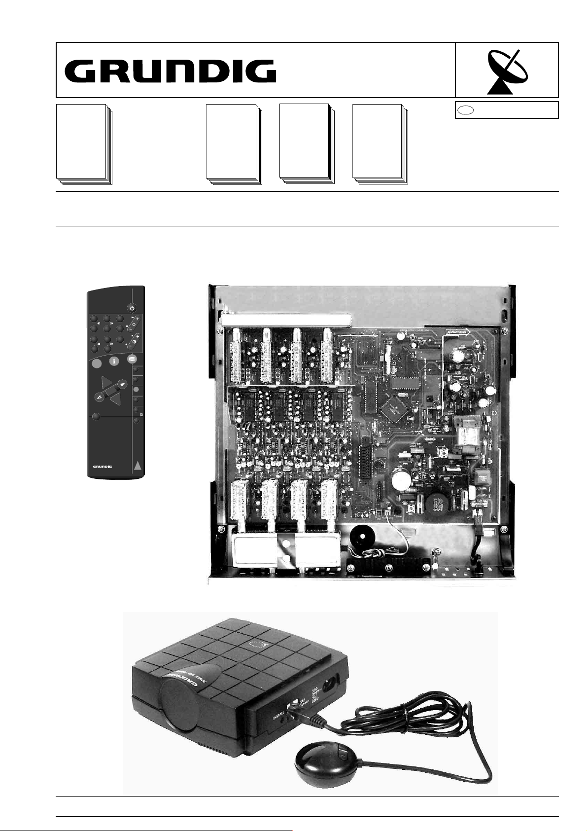
STC 43/45
PLM 40
User
D
Btx * 32700
#
Manual
STC 43/45
PLM 40
Sach-Nr./Part No.
21494-941.02
STC 43, 45, 4/0
PLM 40
STC 4/0 (9.21634-0159 / G.AC 4500)
PLM 40 (9.28016-3870 / G.AY 7900)
PLM 40
TP 720
SAT
Änderungen vorbehalten Printed in Germany Service Manual Sach-Nr.
Subject to alteration VK 22/1 1196 Service Manual Part No. 72010-019.70
Page 2
Allgemeiner Teil / General Section STC 43/45
Es gelten die Vorschriften und Sicherheitshinweise gemäß dem Service Manual "Sicherheit",
Sach-Nummer 72010-800.00, sowie zusätzlich
die eventuell abweichenden, landesspezifischen
Vorschriften!
D
Inhaltsverzeichnis
Seite
Allgemeiner Teil ................................... 1-1…1-4
Bausteinübersicht ........................................................................ 1-2
Technische Daten ........................................................................ 1-3
Schaltplansymbole ....................................................................... 1-3
Service- und Sonderfunktionen .................................................... 1-4
Funktionsbeschreibung ...................... 2-1…2-3
Funktionsbeschreibung ................................................................ 2-1
Abgleich ......................................................... 3-1
Platinenabbildungen .......................... 4-1…4-20
und Schaltpläne
Schaltplan Power Line Modem .................................................... 4-1
Schaltplan SAT-Mouse ................................................................ 4-2
Chassisplatte Power Line Modem ............................................... 4-3
Chassisplatte Kopfstation ............................................................ 4-3
Schaltplan Kopfstation Teil A ..................................................... 4-11
Schaltplan Kopfstation Teil B ..................................................... 4-15
Oszillogramme ........................................................................... 4-18
Eingangsverteiler 29502-016.62 ................................................ 4-19
Ausgangssammler 29502-016.61 .............................................. 4-19
The regulations and safety instructions shall be
valid as provided by the "Safety" Service Manual,
part number 72010-800.00, as well as the
respective national deviations.
GB
Table of Contents
Page
General Section .................................... 1-1…1-4
Module List ................................................................................... 1-2
Specifications ............................................................................... 1-3
Circuit Diagram Symbols ............................................................. 1-3
Service and Special Functions..................................................... 1-4
Funktionsbeschreibung ...................... 2-4…2-6
Circuit Description ........................................................................ 2-4
Alignment....................................................... 3-1
Layout of the P.C.B. ........................... 4-1…4-20
and Circuit Diagrams
Circuit Diagram Power Line Modem ............................................ 4-1
Circuit Diagram SAT-Mouse ........................................................ 4-2
Chassis Board Power Line Modem .............................................. 4-3
Chassis Board Head Station ........................................................ 4-3
Circuit Diagram Head Station Part A ......................................... 4-11
Circuit Diagram Head Station Part B ......................................... 4-15
Oscillogrammes ......................................................................... 4-18
Input Distributor 29502-016.62 .................................................. 4-19
Active Output Collector Field 29502-016.61 .............................. 4-19
Ersatzteillisten ...................................... 5-1…5-4
Spare Parts Lists .................................. 5-1…5-4
Bausteinübersicht / Module List
Gerät
Model
STC 4/0 29702-338.18 29504-201.74
STC 43 29702-338.10 29504-201.74 29502-025.37 - 29502-016.62 29502-016.61
STC 45 29702-338.09 29504-201.74 29502-025.36 - 29502-016.62 29502-016.61
Chassis SAT-Tuner Modulator
29502-025.37
oder/or
29502-025.36
SAT-Mouse
- 29502-016.62 29502-016.61
Eingangssverteiler
Input Distributor
Ausgangssammler
Active Output
Collector Field
PLM 40 29501-060.64 - - 29633-836.01 - -
1 - 2 GRUNDIG Service
Page 3

STC 43/45 Allgemeiner Teil / General Section
Technische Daten
Kanalzüge ....................................................................................... 4
durch Einhängen der Erweiterungseinheit STC 4/0 ........................ 8
SAT-Eingänge (H+V) mit Multiswitcher...................................... 1…4
Empfangsfrequenzbereich ........................................ 950...2150MHz
Eingangspegelbereich ...................................................56...86dBµV
ZF-Bandbreite ........................................... 18 / 27MHz, umschaltbar
Video-Polarität .................................... positiv / negativ, umschaltbar
Videohub ................................................ 16 / 22,5MHz, umschaltbar
Audio ............................................. Hauptträger / Sub-Mono / Stereo
Tonträger ................................................................ Panda-Wegener
Ton-Deemphasis umschaltbar ............................... 50µs / 75µs / J17
Tonauswahl ............................................ Mono / Stereo / 2-Kanalton
Frequenzbereich ..................................... 5,00...9,77MHz, einstellbar
LNC-Power 1 Satellitenantenne ...................... 13V-400mA / 18V-1A
LNC-Power mehrere Satellitenantennen ........ 14V-400mA / 18V-1A
LNC-Schaltsignal .................................................................... 22kHz
Decoderanschluß ....................................................Euro-AV-Buchse
Modulator ........................................ 4 Stück, 2 Seitenband PAL B/G
Ausgangskanäle VHF (STC 43) ......................................... S4…S25
Ausgangskanäle UHF (STC 45) ...................................... C21…C65
Stellbereich Ausgangspegel .....................80…100dBµV, einstellbar
Normen ............................................................................... PAL B/G
Netzspannung ................................................................. 220…240V
Netzfrequenz ...................................................................... 50 / 60Hz
Leistungsaufnahme .............................................................. ca. 35W
Standby ............................................................................... ca. 9,5W
Zulässige Umgebungstemperatur ........................... -10˚C bis + 50˚C
Abmessungen (BxHxT) ...................................... 412 x 394 x 109mm
Gewicht .............................................................................. ca. 7,3 kg
Specifications
Channel lines .................................................................................. 4
by fitting the add-on unit STC 4/0 ................................................... 8
SAT IF-inputs (H+V) with Multiswitch ........................................ 1…4
Input frequency range ............................................... 950...2150MHz
Input level range ............................................................56...86dBµV
IF bandwidth ................................................ 18 / 27MHz, switchable
Video polarity ..................................... positive / negative, switchable
Video deviation ......................................... 16 / 22.5MHz, switchable
Audio .............................................. main carrier / sub-mono / stereo
Sound carrier .......................................................... Panda-Wegener
Sound de-emphasis, switchable ............................ 50µs / 75µs / J17
Sound selection ............................ Mono / Stereo / 2-channel sound
Frequency range ......................................5.00...9.77MHz adjustable
LNC power 1 satellite antenna ........................ 13V-400mA / 18V-1A
LNC power more satellite antennas ................ 14V-400mA / 18V-1A
LNC switching signal ............................................................... 22kHz
Decoder connection ................................................. Euro-AV-socket
Modulator .......................................... 4 pieces, 2 sideband PAL B/G
VHF output channels (STC 43) ........................................... S4…S25
UHF output channels (STC 45) ......................................... C21…C65
Output level ................................................80…100dBµV adjustable
Standards ............................................................................ PAL B/G
Mains supply ................................................................... 220…240V
Mains frequency ................................................................. 50 / 60Hz
Power consumption ............................................................. ca. 35W
Standby ............................................................................... ca. 9.5W
Permissible ambient temperature .............................. -10˚C to +50˚C
Dimensions (WxHxD) ......................................... 412 x 394 x 109mm
Weight ................................................................................ca. 7.3 kg
AFC
AUDIO-L
AUDIO-R
CS
EX
FBAS
NF
RXD
TXD
Schaltplansymbole / Circuit diagram symbols / Symboles schema /
Simboli sullo schema / Simbolos en los esquemas
D
AFC - Spg. / AFC volt. / Tensione de AFC / Tens. AFC / Tensión de
AFC
Audio-Signal links / Audio signal left / Signal audio gauche / Segnale
audio sinistra / Señal audio izquierda
Audio-Signal rechts / Audio signal right / Signal audio droit Segnale
audio destra / Señal audio derecha
Chip-Auswahl / Chip select / Selection chip / Selezione chip /
Elezzión chip
Videosignal-Erkennung / Identification of the videosignal /
Identification du signal video / Identificazione segnale video /
Identificación de señal video
FBAS-Signal / CCVS Signal / Signal video composite / Segnale
video composito / Señal video compuesta
Niederfrequentes Tonsignal / Low Frequency Sound Signal / Basse
frequence/ Tono segnale BF / Señal de sonido de frecuencia baja
Empfangs- und Sendeleitung für seriellen Datenbus / Receive and
transmit lead for serial data bus / Ligne de reception et d'emission
pur datas bus / Ricezione e linea di trasmissione per dati bus / Linea
de transmisión i recepción para bus de datos de serie
GB F
SDA
SCL
TON ZF
22kHz
U
AV
14V
U
18V
U
22kHz
I E
I2C Clock - I2C Bus
Daten / Data / Données / Dati / Data
Ton-ZF-Signal / Sound IF Signal / Signal son FI / Segnale tono FI /
Señal de sonido FI
22kHz Umschaltfrequenz / 22kHz switching frequency / Frequence
de commut. 22kHz / Commut. frequenza 22kHz / Frecuencia de
conm. de 22kHz
Schaltspg. AV / Switching volt. AV / Tens. de commut. AV / Tens. di
commut. AV / Tens. conmut. AV
Schaltspg. 14/18V / 14/18V switching volt. / Tens. de commut. 14/
18V / Tens. di commut. 14/18V / Tens. de conmut. 14/18V
22kHz Schaltspg. / 22kHz switching volt. / Tens. commut. 22kHz /
Tens. commut. 22kHz / Tens. de conm. 22kHz
GRUNDIG Service 1 - 3
Page 4

Allgemeiner Teil / General Section STC 43/45
Sonder- und Servicefunktionen
1. Initialisierung des µP IC870
Nach Wechsel des Prozessors muß der rechnerinterne EEPROM
initialisiert werden.
Dazu müssen Sie Pin 2 des Prozessors IC870 vor dem Einschalten
über die Brücke 836 nach Masse legen. Dadurch wird das EEPROM
im µP geladen.
2. Test der Übertragung und Übertragungsstrecke
1. Durch Schließen der Brücke BR816 an CIC820-(23) sendet
IC800-(16) einmalig ein Datenprotokoll zum Power Line Modem.
Damit kann die Übertragung der Datenprotokolle auch ohne µP
IC870 an IC800-(16) mit dem Oszilloskop getestet werden.
2. Nach dem Einschalten können Sie an der Kopfstation durch Eingabe der Codenummer 8501 dauernde Datenprotokolle im Abstand
von 1 Sekunde senden und damit die Übertragungsstrecke mit
einem Serviceadapter messen.
3. Ein Serviceadapter mit einer Meßeinrichtung über die Größe der
Datenprotokolle ist im Kundendienst in Kürze zu beziehen.
3. Festlegung der Übertragungskanäle
Nach dem Einschalten werden an der Kopfstation durch Eingabe der
Codenummer 8500 definierte Ausgangskanäle belegt, meßbar im
Menü am Ausgang Line 1.
STC 43: Line 1, Kanal 5;
Line 2, Kanal 7;
Line 3, Kanal 9;
Line 4, Kanal 11;
STC 45: Line 1, Kanal 21;
Line 2, Kanal 23;
Line 3, Kanal 25;
Line 4, Kanal 27;
Nach dem Ausschalten wird wieder die kundenspezifische Programmierung eingestellt.
4. Programmierung der Kopfstation
Um gleiche Programmbelegung mehrerer Kopfstationen bzw. der
Erweiterungseinheit zu erreichen, können Sie die Kopfstation mittels
eines PCs über ein Interface an der 4-pol. Buchse BU820 programmieren.
Über diese Schnittstelle läßt sich auch der neueste Softwarestand des
Flash-EEPROM, IC880 einspielen.
Der Adapter und das Programm sind im Kundendienst in Kürze zu
beziehen.
5. Aufruf des Service Menü/Händlerinstallation
Für den Fachhandel ist in der Kopfstation der Infrarotemfänger IC830
eingebaut. Mit der Fernbedienung kann im Menü des Monitors über die
Antennenbuchse der Line 1 von außen mit der Taste "i" –> "Service"
–> "Codenummer 8500" das Menü "Händlerinstallation" aufgerufen
werden.
6. Einstellung der Eingangsparameter
Wenn trotz exakter Abstimmung des Tuners der Linie 2, 3 oder 4 die
Bildqualität nach dem Abspeichern ungenügend ist, muß der Tuner
der Linie 2, 3 oder 4 gewechselt werden.
Grund:
Auch wenn Sie im Menü auf Line 2, 3 oder 4 umschalten, stimmen Sie
immer den Tuner der Line 1 ab und übertragen diese Werte auf die
gewünschte Linie.
Special and Service Functions
1. Initialization of the µP IC870
The EEPROM integrated in the processor must be initialized when the
processor is replaced.
For this, before switching on, connect Pin 2 of the processor IC870 to
chassis via the bridge 836. The EEPROM in the processor will be
loaded.
2. Transmission and Transmisson Channel Test
1. When closing the bridge BR816 at CIC820-(23), IC800-(16) sends
a data protocol once to the Power Line Modem. This makes it
possible to test the transfer of the data protocol at IC800-(16) with
an oscilloscope even without the µP IC870.
2. Having switched on the head station it is possible, by entering the
code number 8501, to send continuoulsy data protocols at a cycle
of 1second and consequently to measure the transmission channel
with a service adapter.
3. A service adapter with a facility for measuring the amplitude of the
data protocols will soon be available from the customer service.
3. Programming of the Transmission Channels
Having switched on the head station and entering the code number
8500 defined output channels will be loaded which are measurable
under the menu on output Line 1.
STC 43: Line 1, channel 5;
Line 2, channel 7;
Line 3, channel 9;
Line 4, channel 11;
STC 45: Line 1, channel 21;
Line 2, channel 23;
Line 3, channel 25;
Line 4, channel 27;
When switching off, the channels programmed by the user will be
reloaded.
4. Programming of the Head Station
For entering the same data into several head stations or an expansion
unit, the head station can be programmed by means of a PC via an
interface at the 4-pin socket BU820.
This interface allows also to load the latest software status of the FlashEEPROM, IC880.
The adapter and the programme will soon be available from the
customer service.
5. Calling up the Service Menu/Dealer Installation Menu
For the specialized dealer, the head station is fitted with the infrared
receiver IC830. The Dealer Installation menu can be called up by
means of the remote control under the menu of the monitor via the
antenna socket of Line 1 with button "i" –> "Service" –> "Code nummer
8500".
6. Setting the Input Parameters
If the picture quality proves to be poor after having stored the tuning
values although the tuner of Line 2 or 3 or 4 has been precisely
adjusted, the tuner of Line 2, 3 or 4 must be exchanged.
Cause:
Even if you switch over to Line 2, 3 or 4 under the menu, it will always
be the Line 1 tuner which will be adjusted and the values taken over by
the desired line.
1 - 4 GRUNDIG Service
Page 5

STC 43/45 Allgemeiner Teil / General Section
Funktionsbeschreibung
1. Allgemeines
Die Stereo-Kopfstation besteht aus 4 Satellitenempfangseinheiten in
einem Gehäuse mit je 199 TV- und 99 Radioprogrammplätzen. Damit
können bis zu vier Teilnehmer einen oder mehrere Satelliten über die
bereits vorhandene Antennenverteileranlage empfangen.
Die Ausgangskanäle können bei der STC 43 (VHF) zwischen S3 und
S24 incl. C5…C12 und bei der STC 45 (UHF) zwischen C21 und C65
eingestellt werden.
Jedem Teilnehmer wird einer dieser Ausgangskanäle zugeteilt. Er
kann mit der Fernbedienung individuell das ihm zugewiesene
Empfangsmodul bedienen. Somit sind für ihn alle Programme des
entsprechenden Satelliten empfangbar.
An der vom Benutzer zugewiesenen Line 4 kann über die EURO-AVBuchse AV1 ein Decoder angeschlossen werden.
Die "SAT-Mouse" empfängt die Infrarot-Steuersignale und leitet die
Fernbedienbefehle mittels eines "Power Line Modems" über das
normale 230 Volt Netz an die zentrale Kopfstation. Das Modem kann
an jede beliebige Steckdose angeschlossen werden.
An die Anlage können Sie 4 Empfangsgeräte, TV oder Videorecorder,
in einer beliebigen Kombination und in verschiedenen Räumen anschließen.
2. Netzteil
2.1 Power Line Modem
Das Schaltnetzteil arbeitet nach dem Sperrschwingerprinzip. Die
Schwingfrequenz liegt bei 70kHz. Die Ausgangsspannung von 9V ist
nach der Gleichrichtung über D1530 kurzschlußfest.
2.1.1 Anlauf
Der Drainanschluß des Schalttransistors T3030 liegt über der Primärwicklung 1/4 des Sperrschwingertrafos T3030 an der gleichgerichteten Netzspannung (D3043…D3046) von ca. 300V. Überschreitet die
Spannung am Gate des T3030 über R3030, R3031 den Wert von 3V,
fließt Strom im Transistor. Das sich aufbauende Magnetfeld im Sperrschwingertrafo induziert in der Wicklung 2/3 eine Spannung und damit
an CC3031. Der Transistor schaltet voll durch.
Übersteigt der Spannungsabfall am Emitter CT3032 über R3032 die
Schaltschwelle des Transistors, schaltet er durch und legt das Gate
des T3030 an Masse. Das Magnetfeld bricht zusammen. T3031 bildet
mit CT3032 einen Thyristor. Damit wird die Schaltung schneller und
niederohmiger. Durch die Induktionsspannung wird das Gate über
C3031 negativ und sperrt T3030 bis das Magnetfeld abgebaut ist.
Gleichzeitig wird auch der Thyristor T3031, CT3032 stromlos und
sperrt. Ist das Magnetfeld im Trafo abgebaut, beginnt ein neuer Anlauf
über R3030, R3031. Die Diode D3038 ist zum Schutz des Transistors
T3030 eingefügt.
2.1.2 Überspannungsschutz
Die Suppressor-Dioden D3031 und D3041, BZT03 D180 mit einer ZSpannung von 180V liegen parallel zum Transformator und dienen als
Überspannungsschutz.
2.1.3 Regelung
Die Betriebsspannung zur Regelung der Ausgangsspannung an dem
Regelverstärker CT3033 wird über die Wicklung 3/2, D3034 erzeugt.
Die Diode D3035 stabilisiert die Regelung. Der negative Anteil der
Regelspannung gelangt über die Diode D3036 an die Basis des
CT3033 und regelt über CT3032 den Schalttransistor.
Für den PLT-IC3010 muß die 9V Betriebsspannung VCC exakt
eingehalten werden. Deshalb liegt parallel zur Basis des Regelverstärkers CT3033 ein weiterer Regelkreis mit dem Optokoppler
OK3030 und D3037.
Bei steigender Spannung VCC sinkt die Spannung am OK3030-(2)
und die LED im Optokoppler leuchtet heller. Die Emitter-Kollektorstrecke zwischen Pin 4 und Pin 5 wird niederohmiger. Damit steigt die
negative Basisspannung an der Basis des CT3033 und über CT3032
wird die Leitzeit des Transistors T3030 kürzer. Die Spannung VCC
wird niedriger.
Fällt die Spannung VCC ist der Regelvorgang umgekehrt und die 9V
steigt.
2.1.4 Sekundärseite
Die Wicklung 5/6 erzeugt die Spannung VCC über D1530 während der
Sperrphase.
IC3033 stabilisiert die 5V Spannung für den µP.
2.2 Kopfstation
Das Schaltnetzteil stellt alle Versorgungsspannungen bereit und kann,
falls erforderlich, bis zu vier LNCs versorgen.
2.2.1 Normalbetrieb / Regelbetrieb
Zur Stromversorgung des Gerätes wird ein freischwingendes Sperrwandlernetzteil mit einer variablen Schaltfrequenz verwendet (120130kHz bei Normalbetrieb und ca. 91kHz bei max. Last und einer
Netzspannung von 190V).
Der Drain-Anschluß des Leistungstransistors T644 liegt über die
Primärwicklung 5/1 des Sperrwandlertrafos TR600 an der gleichgerichteten Netzspannung, D620. Am Ladeelko C626 steht bei 230V
Netzspannung ca. +320 V.
Die Ansteuerung sowie die Regel- und Überwachungsfunktionen des
MOS-Leistungstransistors T644 übernimmt das IC630. Die Versorgungsspannung des Regel-ICs (Pin 6) liegt bei 12V. Nach dem
Erreichen der Einschaltschwelle an Pin 6 über den Widerstand R633
und den Kondensator C633 gibt der IC an Pin 5 einen positiven StartImpuls (1µs) von 10Vss ab. Nach dem Anlauf des ICs wird die
Versorgungsspannung über die Diode D654 und die Spule L654 aus
der Wicklung 7/11 des Wandlertrafos gewonnen. Während der
Leitphase des Transistors wird Energie im Übertrager gespeichert und
in der Sperrphase über die Sekundärwicklung abgegeben. Der
IC630-(5) regelt die Frequenz und das Tastverhältnis des Transistors
T644 so nach, daß die Sekundärspannungen weitgehend unabhängig
von Netzspannung, Netzfrequenz und Last stabil bleiben. Die dazu
nötige Information wird aus der Trafowicklung 7/11 über R664, D661,
und CR661, Regler R667 (Einstellung der +5V_G) an IC630-(1)
geliefert. Der den Logikblock ansteuernde Nulldurchgangsdetektor an
Pin 8 (Wicklung 7/11, CR662) erkennt mit dem Nulldurchgang der
anstehenden Spannung von positiven nach negativen Werten, daß
der Transformator entladen ist und gibt die Logik für den Impulsstart
frei.
Der Kondensator C631 an Pin 7 bewirkt ein verzögertes Ansteigen der
Impulsdauer (Soft- Start).
Die Bauteile D647, D648, C647, R647 und C648 begrenzen die
Spannungsspitzen der Überschwinger am Drain des T644.
2.2.2 Überspannungs- und Überlastschutz.
Sollten im Störfall Überspannungen auf der Primärseite auftreten,
spricht die Speisespannungsüberwachung im IC630 (Pin 6, D654,
Wicklung 7/11) an und unterbricht die Ansteuerung des MOS-Transistors T644.
Ist nach Wiederanlauf weiterhin Überspannung vorhanden, wiederholt
sich der ganze Abfragevorgang.
Über die Drain-Stromnachbildung IC630-(2) kontrolliert der Schaltkreis die Ansteuerimpulse für den Schalttransistor T644. Während der
Leitzeit des MOSFET-Leistungstransistors wird das RC-Glied
R631/C632 geladen. Damit liegt die Primärinduktivität an der Primärspannung. Der steigende Primärstrom löst eine steigende Spannung
an Pin 2 aus und ist somit ein Abbild des Primärstromes über den
Transistor T644. Eine Netzvorregelung beruht auf dem gleichen
Prinzip, denn steigt die Primärspannung wird die Pulsbreite (Leitzeit)
kürzer. Bei Überlastung des Netzteils und somit zu hohem Strom durch
den Power-MOS Transistor schaltet das IC630 das Netzteil ab und
arbeitet im Kurzschlußbetrieb (Netzteil taktet).
2.2.3 Netzunterspannung
Im IC630 arbeitet über Pin 3 eine Schutzschaltung gegen Netzunterspannung. Den Ansprechwert bestimmen R628 und CR636. Bei
230V~ beträgt die Teilspannung ca. 1,7V. Unterschreitet diese Spannung an Pin 3 <0,8V (typ. 0,4V) schaltet der IC630 die Ansteuerimpulse ab.
2.2.4 Standby-Betrieb
Im Betriebszustand steht am Drain des T706 eine Spannung von 12V.
Melden sich alle Teilnehmer ab, schaltet das Gerät in Standby.
Der µP IC870-(37) geht auf "High", CT709 schaltet durch und zieht das
Gate des Transistors T706 nach Masse. Damit ist die Spannung
12V_G abgeschaltet. Fehlt die Spannung 12V_G sperrt auch Transistor T707 und schaltet die Spannung 5V_G ab. Weiterhin zieht der
"High"-Pegel an IC870-(37) IC520 über CT4020 nach Masse und
schaltet die LNC-Versorgungsspannung ab.
Die Leistungsaufnahme der Kopfstation wird auf ca. 10W reduziert.
GRUNDIG Service 2 - 1
Page 6
Allgemeiner Teil / General Section STC 43/45
2.2.5 Sekundärspannungen
+33V: Abstimmoberspannung für Tuner und Modulator, wird aus
der Wicklung 12/2 über D702 gewonnen und mit der
Z-Diode D703 und Transistor T705 stabilisiert.
+12V: ungeschaltete Stromversorgung für Schalt-CIC510 und
CIC530 aus der Wicklung 12/4 und D707.
12V_G geschaltete Stromversorgung für das Signalteil aus der
Wicklung 12/4 und der Diode D707 und Transistor T706.
+9V Stromversorgung für den IC800 aus der Wicklung 12/4
über die Diode D707 und stabilisiert durch den Regler
IC710.
+20V Stromversorgung für die LNCs, aus der Wicklung 12/8,
D721.
+5V Dauerspannung u.a. P rozessoren, die EPROMs, Infrarot-
verstärker aus der Wicklung 14/10 über D726 gleichgerichtet und mit D727 von 5V_G entkoppelt.
5V_G Geschaltete Spannung, gewonnen aus der Spannung
+5V für diverse Schaltungsstufen. Diese Spannung wird
mit dem Einsteller R667 auf 5,2V eingestellt.
6
Reference
Voltage
typ. 3V
U
Ref
4
1
Reversal
Point
Correction
Supply
Voltage
Monitoring
U
6Min
6A
Control and
U
R
Overload
Amplifier
Primary
U
u
Supply
Monitoring
3
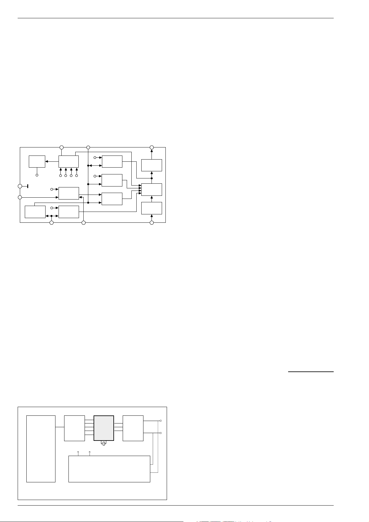
Block Diagram TDA 4605-3
Primary Current
U
2B
Voltage
Converter
U
6Max
U6EU
7
Start Pulse
U
St
Generator
Stop-
Comparator
52
Output and
Current
Control
Logic
Zero
Cross-over
Detector
8
3. Systemsteuerung
3.1 Power Line Modem
Der Infrarotempfänger (SAT-Mouse) decodiert die Fernbedienbefehle
und leitet sie zur Auswertung an den maskenprogrammierten Prozessor CIC3020-(3) im Power Line Modem.
Nach Datenübernahme sendet IC3010-(16) die seriellen Daten an den
Übertrager TR3000 ins Netz zur Kommunikation mit der Kopfstation.
Empfangene Daten von der Kopfstation stehen an IC3010-(2).
3.2 Echolon-Signalübertragung
Der LONWORKS-IC3010 arbeitet als Transmitter-Receiver, das heißt
er sendet und empfängt Daten über das Netz, sodaß keine gesonderten Verbindungsleitungen notwendig sind.
Die Datenprotokolle werden mit einer Frequenz von 133kHz übertragen.
CIC3051 ist zur MegaLogic-Steuerung vorgesehen.
3.3 Kopfstation
Der Prozessor IC870 legt den Programmablauf für die Kopfstation fest
und kommuniziert mit dem Power Line Modem. Das umfangreiche
Steuerprogramm ist im Flash-EPROM IC880 abgelegt. Die veränderbaren Daten wie z.B. Senderfrequenz, Hub oder Tonunterträgerfestlegung sind im vorprogrammierten EEPROM CIC860 Sach-Nr.
72008-668.60 und CIC870 Sach-Nr. 72008-668.61 gespeichert.
Die Datenübertragung zum Power Line Modem koordiniert der
Koprozessor CIC820 mit dem EPROM IC820.
Der LONWORKS-IC800-(16) sendet die seriellen Datenprotokolle mit
einer Frequenz von 133kHz an den Übertrager TR601 ins Netz zur
Kommunikation mit dem Power Line Modem.
Empfangene Daten vom Power Line Modem stehen an IC3010-(2).
Die Parameter im Signalteil werden über den I
2
C-Bus SDA, SCL
eingestellt ebenso wie die Anwahl der gewünschten Lines.
Die Anwahl der jeweiligen Line steuert der µP IC870 über CIC840-(3),
-(13) und IC850-(3), -(13) mit den Befehlen "AFC 1…4" (Automatische
Frequenz Nachstimmung), EX1…4 (Videosignal-Erkennung),
"CS1…4" (Chip Auswahl), SDA1…4 (System Daten).
Die Zeit- und Datumseinstellung übernimmt das Clock-CIC880. Zur
Netzausfallüberbrückung hält der Goldcap-Kondensator C890 ca. 24
Stunden die Spannung an Pin 3.
3.4 LNC-Steuerung
3.4.1 LNC Umschaltung
Die LNC-Spannung ist umschaltbar auf 14V/18V und kann mit einer
Frequenz von 22kHz zur Umschaltung auf verschiedene Satellitenantennen überlagert werden.
Die Umschaltung erfolgt durch den Schaltbefehl "14/18PORT" an
IC504-(13) über CT4030, IC4020.
Eine Schaltspannung an IC870-(36) aktiviert den 22kHz-Oszillator
CIC540 dauerhaft.
3.4.2 DiSEqC Steuerung
Der µP IC870-(36) aktiviert den 22kHz-Oszillator CIC540 je nach
Einstellung im Menü dauerhaft zur Umschaltung eines Koaxrelais.
Stellen Sie im Menü die LNC-Ansteuerung auf die jeweils gewünschte
Antennenkonfiguration 1… 6 mit DiSEqC-Steuerung (Digital Satellite
Equipment Control). Damit wird das 22kHz-Trägersignal mit dem
DiSEqC-Datenpaket (22kHz_PORT) überlagert und schaltet über
T4035, IC4020 den DiSEqC-fähigen Schalter des LNCs. Dazu beide
Eingangsverteiler abziehen und den SAT-Tuner direkt mit dem
Multiswitcher verbinden.
Die DiSEqC 22kHz-Steuersignale enthalten die Information über:
- Polarisation H oder V,
- Wahl des oberen oder unteren Frequenzbereiches eines Quadro-
Band LNCs
- Wahl zwischen zwei Satelliten,
- weitere Schaltmöglichkeiten zur Ansteuerung von max. 4 Satelliten.
Die Antennenanlage muß dann ebenfalls für DiSEqC-Steuerung ausgelegt sein.
Gibt der IC504-(12) an der Leitung "22kHz_PORT" "Low"-Pegel aus,
schaltet der Transistor T4035 durch und die 22kHz Frequenz wird über
IC4020 der LNC-Versorgungsspannung überlagert.
3.4.3 LNC Abschaltung
Sind alle Lines abgemeldet, steht an µP IC870-(37) "High"-Pegel,
CT4050 zieht den Steuereingang Pin 1, IC4020 gegen Masse, schaltet
die LNC-Versorgungsspannung ab und reduziert damit die Leistungsaufnahme der Kopfstation auf 10W.
3.5 Service
Durch Schließen der Brücke BR816 an CIC820-(23) können Sie die
Übertragung der Daten an IC800-(16) mit dem Oszilloskop testen.
Um eine gleiche Programmierung mehrerer Kopfstationen zu erreichen, können Sie mit einer Master Anlage über die 4-pol. Buchse
BU820 eine Data Link-Übertragung durchführen
(Software abhängig).
Für den Fachhandel ist in der Kopfstation der Infrarotemfänger IC830
eingebaut. Mit der Fernbedienung kann am Monitor über die Antennenbuchse an Line 1 von außen mit der Taste "i" –> "Service" –>
"Codenummer 8500" das Menü "Händlerinstallation" aufgerufen werden.
4. Video-Signalweg
Vom Tunerkontakt 6 gelangt das ungeklemmte Basisband-Signal über
eine Invertierungsstufe CT1165 an den Eingang des Video
CIC1170-(20).
Der Video-CIC1170 übernimmt die Aufgaben:
4.1 Amplitudenausgleich von unterschiedlichen Videohüben
Zum Amplitudenausgleich schaltet das Bedienteil den Video-Hub von
16MHz auf 22,5MHz über den I2C-Bus um. Da der Video keine eigene
Anwenderspezifische
Elektronik
Neuron
Chip
5V
PLT-20
Transceiver
9V
Netzteil
Koppel-
schal-
tung
Netzsteck
dose
I2C-Bus-Schnittstelle besitzt, liefert das Ausgangsport des IC503-(8)
die Schaltinformation an Pin CIC1170-(19).
Prinzipschaltung Echolon
2 - 2 GRUNDIG Service
Page 7

STC 43/45 Allgemeiner Teil / General Section
Spannungen an CIC1170-(19)
Hub Spannung
16MHz 2,4V
22,5MHz 3,3V
Für die negativen Video-Einstellungen gelten die gleichen in der
Tabelle angegebenen Spannungswerte. Bei diesen Frequenzhüben
wird lediglich das Videosignal im Tuner invertiert.
4.2 Auswahl des Video-Modus "Linear" bzw. "PAL-Deemphase"
Die Deemphasis wird am Video-IC CIC1170-(2) umgeschaltet. Auslieferungszustand ist PAL-Deemphase ("Low").
Signalweg: CIC1170-(1), CR1172, CIC1170-(3), CR1173, CC1172,
CC1173.
Zur Umschaltung auf "Linear Deemphase" wird der Pin 2 mit +5V
verbunden. Dies geschieht durch Überlöten einer Lötbrücke auf der
Oberseite.
4.3 Klemmung des Video-Signals
Je nachdem wie die Steckbrücken 5 (am Chassis neben dem SATTuner) gesetzt sind, steht an Kontakt 19 der AV-Buchse das Basisband-Signal (CIC1170-(16), CT1052, CT 4200), oder das Videosignal
CIC1170-(14). Das Basisbandsignal wird zur Weiterverarbeitung in
einem Descrambler benötigt.
Dem Klemmeingang CIC1170-(9) ist das Tiefpaßfilter 5MHz F4264
vorgeschaltet. Das geklemmte FBAS-Signal an CIC1170-(14) gelangt
über CT1050 an den Eingang des OSD-Chips IC504-(10) und SyncSeparator CIC501-(6). Vom Ausgang IC504-(8) gelangt das Signal
über CT5502 zum Modulator, Anschluß 5 mit 1Vss.
5. OSD-Einblendung
Die gesamte Bedienung und Einstellungen der Parameter für die
Kopfstation wird über Bildschirmeinblendung über einen 3-LeitungsBus gesteuert. Die Menü-Einblendung übernimmt der BildschirmAnzeige-Steuer-IC504.
Die Bildschirmeinblendung ist in Zeilen- und Spalten aufgeteilt. Die
horizontale und vertikale Bildlage sowie die Zeilenlänge und Spaltenbreite wird im Rechner durch den DOT-Abgleich festgelegt. Zur
Erzeugung der senkrechten Spalten ist der 17MHz-Oszillator an
Pin 16, 17 phasenstarr mit der Zeilenfrequenz verkoppelt. Die Referenzfrequenz zur Synchronisation der Einblendung und des 17MHzOszillators gewinnt der interne Sync-Separator aus dem Videosignal
an Pin 10.
Das Einblendmenü kann mit der grünen Taste auf der Fernbedienung
zwangsweise grün hinterlegt werden.
Bei z.B. schlechtem Empfangs-Signal gibt IC504-(14) über die Leitung
EX 1…4 "High"-Pegel aus und der µP IC870 schaltet den Bildschirm
automatisch grün.
6. Audio-Signalweg
Der Ton-Demodulator IC503 übernimmt die Aufgaben:
6.1 Tonartumschaltung
Der Befehl für die Tonartumschaltung, Mono 50µs / 75µs / J17 / Mono
und Stereo nach Panda Wegener erfolgt über die Leitungen SDA, SCL
am Ton-Demodulator IC503-(17), -(18).
6.2 Ton-Demodulation
Vom Video-CIC1170-(18) durchläuft das Basisband-Signal einen
Bandpaß von 5…9,77MHz und wird dann dem Mischereingang des
Audio- Signalprozessors IC503-(3) zugeführt. Dieser IC beinhaltet
einen I2C-Bus-gesteuerten, PLL-kontrollierten VCO (in 10kHz Schritten) und einen Mischer, der die Eingangsfrequenz auf 10,7MHz
umsetzt.
Zwei im IC enthaltene PLL-FM-Demodulatoren sind mit einem Noise
Reduktion System ausgestattet. Beim Hauptton wird dieses System
per Bypaß umgangen. Am Mischerausgang Pin 5 liegen zwei schmalbandige (130kHz) und ein breitbandiges (280kHz) Keramikfilter, die
die Eingänge Pin 9, 11, 13 mit FM-Signal versorgen.
Die regelbaren Audio-Ausgänge L/R IC503-(23), -(22) sind mit der
AV-Buchse, Kontakt 1, 3 und den Eingängen des CIC500-(3), -(5)
verbunden. Er arbeitet als schaltbarer Verstärker und führt das
Audiosignal L und R an den Stereocoder-IC TDA 6621.
6.3 Verstärkungsregelung
Die Verstärkung (ca. 3dB) des CIC500 ist schaltbar mit den Transistoren CT5000, CT5004 in Abhängigkeit der Spannung an IC503-(7)
"High" oder "Low".
6.4 Stereo-Coder
Der Stereo-Coder IC501 TDA 6621-(1), -(3) erzeugt L und R bei
Monosendungen, matriziert die Summen- bzw. Differenzsignale (L+R)/2
und R (Stereo) oder Ton 1 und Ton 2 (Zweikanalton) für den Haupt(5,5MHz) und Nebentonträger (5,742MHz) und erzeugt dafür die
entsprechenden Umschaltungen.
6.4.1 Erzeugung der Kennsignale und des Pilottons
Der CIC501 erzeugt aus dem an Pin 6 anliegenden Videosignal die
Sync.-Impulse, mit deren Hilfe die Kennsignale (Mono, Stereo, Zweikanal) für Fernsehgerät oder Videorecorder erkannt werden. Sie sind
nur im Nebentonträger (5,742MHz) vorhanden.
Dazu wird dieser mit 54,6875kHz, der 3,5-fachen Zeilenfrequenz,
frequenzmoduliert. Die 54,6875kHz selbst werden wiederum mit
117,5Hz (Stereo) oder 274,1Hz (Zweikanal) amplitudenmoduliert.
Bleibt der Pilotton von 54,6785kHz unmoduliert, handelt es sich um
eine Monosendung.
An Pin 15 liefert der IC501 rechteckige Kennsignale für die gewünschte Betriebsart 117,5Hz oder 274,1Hz. Nachdem das Signal den
schaltbaren Bandpaß CIC502 durchlaufen hat, steht es wieder an
IC501-(16) und wird als Kennton dem Pilottonträger aufmoduliert.
Der Pilotton 54,6874kHz an IC501-(5) wird mit dem aus dem FBASSignal CIC501-(6) gewonnenen Sync-Impuls synchronisiert, zum NFSignal 2 addiert und über den Einsteller R5004 dem Modulator
zugeführt.
Der Bus legt über IC502 an IC501-(12), -(13) den gewünschten Mode
fest.
Pin 12 Pin 13 Mode
Low Low Mono
Low High Stereo
High Low Zweikanal
Mit den Einstellern R5002 und R5006 wird in der Fertigung der
Frequenzhub eingestellt. Zur Einstellung ist ein SAT-Sender mit
definiertem Hub erforderlich.
7. Decoderbetrieb
Zum Entschlüsseln von verscrambelten Programmen kann an der AVBuchse ein Decoder angeschlossen werden.
Das an Kontakt 19 der AV-Buchse stehende Basisband-Signal wird im
Decoder entschlüsselt und über Buchsenkontakt 20, CT580, CT 582
und Umschalter CIC510-(12), -(14) zur Weiterverarbeitung an den
Eingang IC504-(10) geführt.
Das Audio Signal gelangt über Buchsenkontakt 1 und 3, Umschalter
CIC510, Verstärker CIC530-(2), -(5) zur Weiterverarbeitung an den
Stereocoder IC501.
Die Umschaltspannung an Buchsenkontakt 8 für den CIC510 liefert
der Decoder, oder der µP IC870-(35), CT502, CT500, CR506, CIC510(9), -(10), -(11) durch eine Zwangsumschaltung.
GRUNDIG Service 2 - 3
Page 8

Allgemeiner Teil / General Section STC 43/45
Functional Description
1. General
The Stereo Head Station is made up of 4 satellite frontend modules in
one encapsulation providing 199 TV and 99 radio memory locations
each so that a maximum of four subscribers can receive one or more
satellites via the existing aerial distribution system.
The output channels can be set between S3 and S24 incl. C5 ... C12
with the STC 43 (VHF) head station, and between C21 and C65 with
STC 45 (UHF).
One of these output channels is allocated to one subscriber who then
is able to operate the frontend module allocated to him individually by
means of the remote control. The subscriber can consequently receive
all programmes of the respective satellite.
Line 4 which is allocted to the user can be connected to a decoder via
the EURO-AV socket AV1.
The "SAT-Mouse" receives the infra-red control signals and passes
these remote control commands on via a "Power Line Modem" and the
usual 230 Volt mains to the central head station. The modem can be
connected to any socket outlet.
The system allows to connect 4 receivers, TV's or video recorders in
any combination and in different rooms.
2. Power Supply
2.1 The Power Line Modem
The switched mode power supply operates on the principle of a
blocking oscillator. The oscillation frequency is 70kHz. After rectification via D1530 the 9V output voltage is short circuit proof.
2.1.1 The Start-up
The drain of the switching transistor T3030 is connected via the primary
winding 1/4 of the blocking oscillator type transformer T3030 to the
rectified mains voltage (D3043…D3046) of 300V approximately. If the
voltage supplied via R3030, R3031 to the gate of T3030 exceeds the
3V level, current starts to flow in the transistor. The building up
magnetic field in the blocking oscillator type transformer induces a
voltage in the winding 2/3 and along with it in CC3031. The transistor
switches on fully.
If the voltage drop on R3032 exceeds the switching threshold at the
emitter CT3032 of the transistor, the transistor turns on and switches
the gate of T3030 to chassis potential. The magnetic field breaks down.
T3031 and CT3032 form a thyristor so that the switching is carried out
faster and at lower resistance. The induction voltage causes the gate
to become negative via C3031 and turns off T3030 until no magnetic
field is left in the transformer. At the same time, no current is present
at the thyristor T3031, CT3032 so that it switches off. As soon as the
magnetic field is completely transferred from the transformer, a new
cycle is started via R3030, R3031. The diode D3038 is used to protect
the transistor T3030.
2.1.2 The Overvoltage Protection
To protect the transformer from impermissibly high voltage levels, the
Suppressor Diodes D3031 and D3041, BZT03 D180, with a Z-voltage
of 180V are connected in parallel with it.
2.1.3 The Control
The operating voltage for controlling the output voltage at the gain
controlled amplifier CT3033 is produced via the winding 3/2, D3034.
The diode D3035 serves for holding stable the operating voltage. The
negative component of the control voltage is fed through diode D3036
to the base of CT3033 and controls the switching transistor via
CT3032.
The 9V operating voltage VCC for PLT-IC3010 must be controlled very
precisely. For this, an addtional control circuit with the optocoupler
OK3030 and D3037 is connected in parallel with the base of the control
amplifier CT3033.
When the voltage VCC increases the voltage at OK3030-(2) decreases and the LED within the optocoupler becomes brighter. The
emitter-collector path between Pin 4 and Pin 5 becomes low resistance. Consequently, the negative base voltage at CT3033 increases
and the conducting phase of T3030 becomes shorter via CT3032. The
voltage VCC falls.
With the falling VCC voltage the control process reverses and the 9V
supply increases.
2.1.4 The Secondary
The VCC voltage is generated by the winding 5/6 via D1530 during the
"off" phase.
IC3033 is used to hold stable the 5V supply for the µP.
2.2 The Head Station
The switched mode power supply delivers all supply voltages and can
supply up to four LNC's.
2.2.1 Normal / Controlled Operation
For the power supply of this satellite TV converter a free running
Blocking Oscillator Converter Power Supply with variable switching
frequency is used (on normal operation approx. 120-130kHz and
approx. 91kHz at maximum load and a mains voltage of 190V).
The drain contact of the power transistor T644 is connected via the
primary winding 5/1 of the blocking oscillator transformer TR600 to the
rectified mains voltage, D620. At a mains voltage of 230V the voltage
level present at the charging electrolytic capacitor C626 is approx.
+320V.
The IC630 is responsible for driving, controlling and monitoring the
MOS power transistor T644. The supply for the control-IC is 12V and
is present on Pin 6. As soon as the switch-on threshold is reached on
Pin 6 via the resistor R633 and the capacitor C633, the IC feeds out a
positive start pulse (1µs) of 10Vpp on Pin 5. After start-up of the IC, the
supply voltage is obtained via the diode D654 and the coil L654 from
the winding 7/11 of the blocking oscillator transformer. During the
conducting phase of the transistor, energy is stored in the transformer
and this is transferred into the secondary winding when the transistor
is switched off. The IC630-(5) varies the frequency and the period
during which the transistor T644 is switched on, so that the secondary
voltages are stable and are largely not affected by variations in the
mains supply, mains frequency and the load. For this to be carried out
the necessary information is taken from the transformer winding 7/11
via R664, D661 and CR661, as well as the adjustment control
R667(adjustment of the +5V_G) to IC630-(1). The zero cross-over
detector on Pin 8 (winding 7/11, CR662), which drives the logic block,
knows by the voltage passing through zero from positive to negative
that the transformer is discharged and enables the logic block to
produce the start pulse.
The capacitor C631 on Pin 7 delays the rise of the pulse start duration
(soft start).
The components D647, D648, C647, R647 and C648 are used to limit
the voltage peaks in the overshoots at the drain of T644.
2.2.2 Overvoltage and Overload Protection
If due to a fault condition overvoltages occur at the primary winding, the
supply voltage monitoring circuit in IC630 (Pin 6, D654, winding 7/11)
responds and interrupts the drive to the MOS transistor T644.
If after restart, the overvoltage condition is still present, the complete
sampling process is repeated.
By means of a drain current simulation on IC630-(2) the circuit monitors
the driving pulses to the switching transistor T644. During the conducting period of the MOSFET power transistor the RC-network R631 /
C632 is charged up. Consequently, the primary inductivity is connected to the primary voltage. The increasing primary current causes
the voltage on Pin 2 to rise as well which thus represents the primary
current via the transistor T644. A preliminary mains control works on
the same principle: with the rising primary voltage the pulse period
(conducting period) is reduced. When the power supply is overloaded
and as a result too high a current is flowing through the Power-MOS
transistor, the IC630 switches the power supply off and operates in
short-circuit mode (power supply is pulsated).
2.2.3 Mains Undervoltage
In IC630 a protection circuit operates via Pin 3 when mains undervoltages occur. The threshold value is determined by R628 and
CR636. At a mains voltage of 230V a.c. the component voltage is
approx. 1.7V. When this voltage on Pin 3 is < 0.8V (typically 0.4V), the
IC630 switches the drive pulses off.
2.2.4 Standby Mode
In normal operating mode, a voltage of approx. 12V is present on the
drain of T706. When all subscribers to the head station are "off", the
head station switches to standby.
The µP IC870-(37) switches to “High”, CT709 switches through and
pulls the gate of the transistor T706 to chassis potential. As a result, the
voltage 12V_G is switched off. The missing voltage 12V_G causes the
2 - 4 GRUNDIG Service
Page 9

STC 43/45 Allgemeiner Teil / General Section
transistor T707 to turn off and so does the 5V_G voltage. Additionally,
the "High" level on IC870-(37) pulls IC520 to chassis potenial via
CT4020 and turns off the LNC supply.
The power consumption of the head station is reduced to 10W
approximately.
2.2.5 Secondary Voltages
+33V: the tuning upper limit voltage for the tuner and modulator
is generated from winding 12/2 via D702 and held stable
by means of the Z-diode D703 and transistor T705
+12V: unswitched supply for the switch-CIC510 and CIC530
from the winding 12/4 and D707
12V_G switched supply for the Signal Processing circuit from the
winding 12/4 and diode D707 and transistor T706
+9V supply for IC800 generated from the winding 12/4 via
diode D707 and stabilized by control IC710
+20V supply for the LNC's, from winding 12/8, D721
+5V unswitched supply voltage, among others for the proces-
sors, EPROM's, infrared amplifier; obtained from winding
14/10, rectified via D726, and decoupled with D727 from
5V_G
5V_G switched supply, derived from the +5V supply for various
circuit sections. This supply is set with control R667 to
5.2V
6
Reference
Voltage
typ. 3V
U
Ref
4
1
Reversal
Point
Correction
Supply
Voltage
Monitoring
U
6Min
6A
Control and
U
R
Overload
Amplifier
Primary
U
u
Supply
Monitoring
3
Block Diagram TDA 4605-3
Primary Current
U
2B
Voltage
Converter
U
6Max
U6EU
7
Start Pulse
U
St
Generator
Stop-
Comparator
52
Output and
Current
Control
Logic
Zero
Cross-over
Detector
8
3. System Control
3.1 Power Line Modem
The infrared receiver (SAT Mouse) decodes the remote control commands and passes them on for evaluation to the mask-programmed
processor CIC3020-(3) within the Power Line Modem.
On completion of the data transfer, IC3010-(16) sends the serial data
to the transformer TR3000 to be fed into the network for communication with the head station.
Data received from the head station are applied to IC3010-(2).
3.2 Echolon Signal Transmission
The LONWORKS-IC3010 works as a transmitter/receiver, transmitting and receiving data via the network so that extra connecting leads
are not necessary.
The data protocols are transferred at a frequency of 133kHz.
CIC3051 is provided for MegaLogic control.
3.3 Head Station
The processor IC870 determines the sequence of operations for the
head station and communicates with the Power Line Modem. The
extensive control programme is stored in the Flash-EPROM IC880.
The variable data, for example transmitter frequency, deviation or
PLT-20
Transceiver
9V
Power Supply
Coupling
Circuit
Power
Mains
User's
Application
Electronics
Echolon Basic Circuit
Neuron
Chip
5V
sound subcarrier, are stored in the pre-programmed EEPROM CIC860
part no. 72008-668.60 and CIC870 part no. 72008-668.61.
The data transfer to the Power Line Modem is coordinated by the
coprocessor CIC820 with EPROM IC820.
The LONWORKS-IC800-(16) sends the serial data protocols at a
frequency of 133kHz to the transformer TR601 to be fed into the
network for communication with the Power Line Modem.
Data received from the Power Line Modem are applied to IC3010-(2).
The parameters in the signal processing stage are set via the I2C-bus
SDA, SCL and so are the desired lines.
Selection of the respective line is under control of the µP IC870 via
CIC840-(3), -(13) and IC850-(3), -(13) by means of the commands
"AFC 1…4" (Automatic Frequency Control), EX1…4 (Video Signal
Identification), "CS1…4" (Chip Selection), SDA1…4 (System Data).
The Clock-CIC880 is provided for setting the time and date. A possible
power failure is bridged by the goldcap capacitor C890 which maintains the voltage at Pin 3 for approx. 24 hours.
3.4 LNC Control
3.4.1 LNC Switch-over
The LNC can be switched to 14V/18V and can be superimposed with
a frequency of 22kHz for switching over to different satellite dishes.
Switching is effected with the switching command "14/18PORT" at
IC504-(13) via CT4030, IC4020.
A switching voltage at IC870-(36) activates the 22kHz oscillator
CIC540 continuously.
3.4.2 DiSEqC Control
Dependent on the setting under the menu, the µP IC870-(36) activates
the 22kHz oscillator CIC540 continuously for switching over a coaxial
relay.
Under the LNC drive menu, select the desired antenna configuration
1 ... 6 with DiSEqC (Digital Satellite Equipment Control) under the LNC
drive menu. The 22kHz carrier signal will then be superimposed with
the DiSEqC data (22kHz_PORT) and switches over the DiSEqCcapable switch of the LNC via T4035, IC4020. For this disconnect the
input splitter and connect the SAT tuner directly with the multi-switch.
The DiSEqC 22kHz control signals contain information about:
- polarization H or V,
- selection of the upper or lower frequency range of a QuadroBand LNC
- selection between two satellites,
- further switching possibilities to drive a max. of 4 satellites.
The antenna system needs to be designed for DiSEqC control, too, in
this case.
When IC504-(12) feeds out "Low" level at line "22kHz_PORT", the
transistor T4035 switches through and the 22kHz frequency is superimposed via IC4020 on the LNC supply voltage.
3.4.3 LNC Switch-off
When all lines are switched off, a "High" level is applied to µP IC870(37), CT4050 pulls control input Pin 1 of IC4020 to chassis potential,
switches off the LNC supply and reduces the power consumption of the
head station to 10W.
3.5 Service
By closing the bridge BR816 at CIC820-(23) the data traffic can be
tested at IC800-(16) with an oscilloscope.
To enter the same data into several head stations, a Data Link transfer
can be effected with a Master system via the 4-pin socket BU820
(dependent on the software).
For the specialized dealers, the infrared receiver IC830 is provided in
the head station. The "Dealer Installation" menu can be called up from
outside with the remote control on the monitor via the antenna socket
on Line 1 with button "i" –> "Service" –> "Code number 8500".
4. Video Signal Path
From tuner contact 6, the unclamped baseband signal is fed through
an inverting stage CT1165 to the input of the video CIC1170-(20).
This IC takes over the following functions:
4.1 Amplitude Compensation for Different Video Deviations
To compensate for the different amplitudes the keyboard control unit
switches over the video deviation from 16MHz to 22.5MHz via the
I2C-bus. Since the video CIC does not have its own I2C bus interface,
the switching information is supplied by the output port of IC503-(8) to
CIC1170-(19).
GRUNDIG Service 2 - 5
Page 10

Allgemeiner Teil / General Section STC 43/45
Voltages at CIC1170-(19):
Deviation Voltage
16MHz 2.4V
22.5MHz 3.3V
The same voltage levels given in the table apply to the negative video
deviations. In this case the video signal is simply inverted within the
tuner.
4.2 Selection of the Video Mode "Linear" or "PAL Deemphasis"
The deemphasis is switched over at video CIC1170-(2). At the time of
delivery, the system is switched to PAL Deemphasis (Low).
Signal path: CIC1170-(1), CR1172, CIC1170-(3), CR1173, CC1172,
CC1173.
For switching over to "Linear Deemphasis", Pin 2 must be connected
to +5V. This is done by closing the solder bridge on the upper side.
4.3 Video Signal Clamping
Dependent on the setting of the plug-in bridges 5 (located on the
chassis beside the SAT tuner), either the baseband signal (CIC1170(16), CT1052, CT4200), or the video signal CIC1170-(14) is provided
at contact 19 of the AV-socket. The baseband signal is used for further
processing in a descrambler.
The clamping input CIC1170-(9) is preceded by a 5MHz lowpass filter
F4264. The clamped CCVS signal at CIC1170-(14) is fed through
CT1050 to the input of the OSD chips IC504-(10) and the sync
separator CIC501-(6). From output IC504-(8) the signal is supplied via
CT5502 to the modulator, Pin 5, at 1Vpp.
5. On Screen Display (OSD)
The total operation and setting of the parameters of the head station
is controlled via the information displayed on the screen via the 3-lead
bus. Insertion of the menu is effected with the on-screen-display
control IC504.
The on-screen-display is subdivided into lines and columns. The
horizontal and vertical position of the picture as well as the line length
and width of the columns is determined within the computer by varying
the DOT oscillator. For generating the vertical columns, the 17MHz
oscillator at Pin 16,17 is phaselocked to the line frequency. The
reference frequency for synchronizing the displayed information and
the 17MHz oscillator is derived from the video signal at Pin 10 by the
internal sync separator.
The background colour of the displayed menu can be forced to Green
by pressing the green button on the remote control.
For example if the signal being received is poor, IC504-(14) feeds out
a "High" level via the lead EX 1…4 and µP IC870 switches the screen
automatically over to Green.
6. Audio Signal Path
The Sound Modulator CIC503 takes over the following functions:
6.1 Switching over the Sound
The command for switching over to Mono 50µs / 75µs / J17 / Mono and
Stereo sound with Panda Wegener is passed on via the I2C-bus to the
sound demodulator IC503-(17), -(18).
6.2 Sound Demodulation
From video CIC1170-(18), the baseband signal is fed through a
5…9.77MHz bandpass to the mixer input of the audio signal processor
IC503-(3). This IC contains a VCO which is tuned (in 10kHz steps) via
the I2C-bus under control of a PLL circuit, and a mixer to convert the
input frequency to 10.7MHz.
Two PLL-FM demodulators within this IC are provided with a Noise
Reduction System. A bypass is provided to circumvent this system for
the main sound carrier. At the mixer output Pin 5, two narrow-band
ceramic filters (130kHz) and one wideband ceramic filter (280kHz) are
used to supply the FM signal to the input pins 9, 11, 13.
The gain-controlled audio outputs L/R IC503-(23), -(22), are connected with contacts 1, 3 of the AV socket, and with the inputs of
CIC500-(3), -(5). It works as a switchable amplifier and passes the L
and R audio signals on to the stereo coder IC TDA 6621.
6.3 Gain Control
The gain (approx. 3dB) of CIC500 can be switched by the transistors
CT5000, CT5004, in dependence of the voltage present at IC503-(7),
to "High" or "Low".
6.4 Stereo Coder
The stereo coder IC501 TDA 6621-(1), -(3) is used for generating the
L and R signals for mono transmissions, for matrixing the sum or
differential signals (L+R)/2 and R (stereo) or sound 1 and sound 2 (twochannel sound) for the main sound carrier (5.5MHz) and sound
subcarrier (5.742MHz) and for generating the necessary switching
voltages for these functions.
6.4.1 Generation of the Ident Signals and the Pilot Tone
The sync signals which are used to recognize the identification signals
(mono, stereo, two-channel sound) for the tv receiver or video recorder
are produced within CIC501 from the video signal applied to Pin 6.
They are only present in the sound subcarrier (5.742MHz).
For this the sound subcarrier is frequency-modulated with 54.6875kHz
which is 3.5 times the line frequency. The frequency of 54.6875kHz is
in turn amplitude-modulated with 117.5Hz (stereo) or 274.1Hz (twochannel sound). If the pilot tone of 54.6785kHz is not modulated, it is
a mono sound transmission.
On pin 15, the IC501 supplies the square-wave ident signals for the
desired operating mode, 117.5Hz or 274.1Hz. Having passed through
the switchable bandpass CIC502, the signal is returned to IC501-(16)
and is modulated as ident sound with the pilot tone carrier.
The 54.6874kHz pilot tone at IC501-(5) is synchronized with the sync
signal obtained from the CCVS signal at CIC501-(6), it is then added
to the AF signal 2, and fed through the adjustment control R5004 to the
modulator.
The desired mode is set via the IC502 at IC501-(12), -(13), via the bus:
Pin 12 Pin 13 Mode
Low Low Mono
Low High Stereo
High Low 2-channel
The adjustment controls R5002 and R5006 are used in the factory to
set the frequency deviation. For this a SAT transmitter with defined
deviation is necessary.
7. Decoder
It is possible to connect a decoder to the AV socket for decoding
scrambled programmes.
The baseband signal present at contact 19 of the AV socket is
descrambled in the decoder and passed through socket contact 20,
CT580, CT582 and the switch CIC510-(12), -(14) to the input IC504(10) for further processing.
The audio signal is taken via socket contact 1 and 3, the switch CIC510,
the amplifier CIC530-(2), -(5) to the stereo coder IC501 for further
processing.
The switching voltage on socket contact 8 for CIC510 is supplied from
the decoder or, by forced switching, from the µP IC870-(35), CT502,
CT500, CR506, CIC510-(9), -(10),-(11).
2 - 6 GRUNDIG Service
Page 11

STC 43/45 Allgemeiner Teil / General Section
D
Abgleich
Alle nicht beschriebenen Filter und Einstellregler sind werkseitig abgeglichen und dürfen im Service-Fall nicht verdreht werden.
Filter müssen im Servicefall durch ein vorabgeglichenes ersetzt werden.
Servicearbeiten nach Austausch bzw. Reparatur:
SAT-Tuner und Peripherie
Abgleich
Videopegel
Vorbereitung
Gerät auf SAT-Empfang (z.B. Satellit Astra) schalten, richtigen Videohub einstellen (Astra 16MHz).
Oszilloskop: IC504-(10)
FBAS-Signal auf Bildfrequenz triggern
Mit dem Einstellregler R1160 die Amplitude der Vertikalaustastlücke im FBAS-Signal auf 2,2Vss einstellen.
Abgleichvorgang
GB
Alignment
All filters and adjustment controls not mentioned in this description are pre-set at the factory and must not be re-adjusted in the case of repairs.
Filters must be replaced in service by a new pre-set one.
Measuring works after replacement or repair:
SAT-Tuner and periphrals
Alignment
Video level
Preparations
Switch the SAT receiver to SAT reception (eg. Astra) and
set the correct video deviation (Astra 16MHz).
Oscilloscope: IC504-(10)
Trigger the CCVS signal to the vertical sync frequency.
With adjustment control R1160 set the amplitude of the
vertical blanking gap in the CCVS signal to 2.2Vpp.
Alignment Process
GRUNDIG Service 3 - 1
Page 12

Allgemeiner Teil / General Section STC 43/45
Notizen / Notes
3 - 2 GRUNDIG Service
Page 13

STC 43/45 Platinenabbildungen und Schaltpläne / Layout of the PCBs and Circuit Diagrams
0,1u
CC1432
560
CR1433
270
CR1432
S1433
DOWNUP
EIN
22k
CR1434
S1434
IR
+5V
1
2
3
TFMS5300
IC1430
BC848B
CT1434
1
2
3
4
5
6
BU1430
TLHR4601
D1433
22k
CR1431
7
8
1
2
3
4
5
6
BU1420
n.v.
+5V/D
+5V/D
+5V/D
291096
IR-EINHEIT SAT-MOUSE 29633-836.01
IR-EMPFANGSPL. 29305-180.01
C. O. RECEPTEUR IR
CHASSIS
PLACA RECEPTOR IR
PIASTRA RICEVITORE IR
IR RECEIVER BOARD
Power Line Modem
STC 43/45 Platinenabbildungen und Schaltpläne / Layout of the PCBs and Circuit Diagrams
8
7
6
5
M
4
3
2
1
BUCHSE1
SOCKET1
IR
3
+5V
TFMS5300
2
1
M
P1
220V-
240V~
SI3001
P1
1,25A/H
POWERLINE MODEM 29501-060.64
LP POWERLINE MODEM 29305-180.07
GRUNDIG Service
+5V
C3006
+
47u/16V
M
F
C3002
29500-833.97
CR3014
100
CR3006
22K
CR3007
270
NUR VORGESEHEN
IF REQUIRED
PREVU
SOLO PREVISTO
SOLAM.PREVISTO
0,1u/MP3/250V_AC
L3040
+5V
+5V
TR3000
13 9
1M
R3002
C3001
F
0,1u/MP3/250V_AC
PRIMAERMASSE / NICHT NETZGETRENNTES SCHALTUNGSTEIL
PRIMARY CHASSIS, NOTE / CIRCUT NOT MAINS ISOLATED
MASSE PRIMAIRE / CIRCUIT NON ISOLE DU SECTEUR
P
MASSA PRIMARIO / CIRCUITO NON SEPAR., DALA RETE
MASA PRIMARIA / SECTOUR DE COM. NO SEP. DE LA RED
F
C3047
0,1u/MP3/250V_AC
62
C3043
1n
1N4007
D3043
1N4007
D3044
C3044
D3039
1N4001
1n
M
M
470p
F
C3003
L3003
CR3002
CR3003
M
CC3010
0,15u
1m
47
33
12u
L3001
C3046
1N4007
D3046
1N4007
D3045
C3045
1N4001
1n
1n
D3040
D3001
D3002
M
C3004
1u
1N5343B
1N5343B
M
C3030
R3032
F
+
P
M
CC3009
4,7n
15
21
16
2
3
10u/400V
4,7
PKD
CM/DM
TXOUT
RXIN
GND
M
CR3012
100
CC3008
4,7n
+VCC
GND
8
1
R3030
1
R3031
D3038
20
VA
GND
2,7M
2,7M
1N4148
+5V
IC3010
L3008
M
CC3031
330
CR3033
CR3011
9
VDD
PLT20
RXCOMP
1
1mH
1n
CR3035
CR3029
CR3034
220k
100
CR3008
12 11
CKSEL1
XIN
Q3008
10MHz
+5V
T3030
BUZ90A
68
100
CT3032
BC848C
4,7K
CR3009
320V
M
CKSEL0
CKOUT
RESET
XOUT
191817
330
P
P
CR3013
4,7K
CR3022
T3031
BC858C
4,7K
CC3012
4
CP4
14
BIN
5
CP2
6
CP1
7
CP0
CR3051
10
13
10K
D3041
D3031
BZT03D180
21
43
CR3036
BA157
P
M
270
4,7n
BZT03D180
D3032
4,7k
4,7n
M
22
21
CP3
17
CP2
20
CP1
19
CP0
15
CLK1
1
RESET
5
TR3030
6
C3032
F
100p/1600V
CR3037
1k
CR3038
CC3011
I00
BYT53D
D3033
I01
CLK2
VSS
14 13
SI3002
T630mA
CC3033
100p
P
CT3033
BC858C
+5V
CR3021
D3021
I03
CIC3020
N3120
VSS
VSS
109
470
CR3020
876 54
SERVICE
VSS
16
M
C3038
BAT43
100
I08
VSS
+
M
1N4148
I07
VSS
31 30
470u/25V
D3034
CR3039
4 - 1
NUR VORGESEHEN
IF REQUIRED
PREVU
SOLO PREVISTO
SOLAM.PREVISTO
292827
26
I09
I06
I02
32
VDD
25
VDD
18
VDD
12
VDD
11
VDD
2
VDD
3
I04
IC10
I05
2423
4,7n
560
R3048
D3035
C3034
ZPD9,1
P
1k
1.5n
CC3035
M
M
M
CC3026
47n
47n
100p
M
CC3024
+5V
M
CC3019
CC3023
47n
CC3025
47n
CR3019
100
M
IC3021
12
MC33164
RESET
3
CC3022
CR3040
10u/50V
M
68k
CR3041
M
2.2k
+
4,7n
M
OK3030
654
P
D3036
1N4148
+
C3036
P
1u/100V
GRUNDIG Service
+5V
10K
CC3027
C3005
K
1n
R3005
1
2,7M
NUR VORGESEHEN
IF REQUIRED
PREVU
SOLO PREVISTO
SOLAM.PREVISTO
10K
CR3070
CR3071
+5V
321
M
10K
CR3072
CR3047
1k
CR3042
680
CR3043
470
10K
+5V
BC847B
CT3060
27K
CR3062
CD3065
CC3051
47n
CC3050
10K
CR3073
CR3074
M
20 21
P3-1
25
P0-0
26
P0-1
27
P0-2
28
P0-3
TxD
19
P3-0
18
RESET
17
VCC
P3-3
22
VREF
VSS
47n
13
P0-5
CIC3051
M37477
IN2
IN3
9101112
16
2930
p0-4
IN1
M
IC3033
CR3044
3,3k
CC3037
47n
CR3045
33k
M
D3037
TL431
MC7805
2
3
CR3046
1.5k
CC3041
M
M
47n
C3042
F
C3040
M
291096
1
0,33u
CC3060
220p
47K
CR3061
BAW56
M
5678
p1-1
p1-2
p1-3
P1-6
P1-7
IN0
1234
+VCC
+5V
+
100u/35V
M
p1-0
RxD
P3-2
P4-0
p0-7
p0-6
p4-1
XOUT
XIN
CR3076
10K
/9V
2,2K
M
23
32
31
24
15
14
CR3060
CR3052
CT3055
1M
+5V
BC847B
220
M
CR3057
CR3056
Q3052
4MHz
220p
100K
22K
CR3055
CC3053
18p
CR3050
CR3058
CC3056
CC3052
18p
0
100
CHINCH
2
100p
1
CC3058
M
+5V
MM
4 - 2
Page 14

Platinenabbildungen und Schaltpläne / Layout of the PCBs and Circuit Diagrams STC 43/45
Platinenabbildungen und Schaltpläne / Layout of the PCBs and Circuit Diagrams STC 43/45
Chassisplatte PLM 40
Chassis Board PLM 40
Bestückungsseite, Ansicht von oben
Component side, top view
CHINCH
X1
7
8
D3002
BUCHSE1
1
2
Keine
Netztrennung
C3002
P1
0 1 2 3 4 5 6 7 8 9
SI3001
7
CR3044
29306-401.07 2L(05)
29306-401.07 4LS(05)
CR3047
CR3040
T3033
CBR19
T3032
CR3038
EB
EB
CR3037
T 1.25A
MP7
MP9
CC3041
CBR18
CR3042
CR3045
CR3043
C3033
T3031
CR3033
CC3027
C3037
CR3041
EB
CR3034
CR3029
C3006
13
U1
29306-401.07 4B(05)
Durchlaufrichtung
L3008
D3001
TR3000
13
14
R3002
L3040
C3047
MP8
CR3046
C3035
CR3035
CR3039
C3031
CR3036
121
69
5
2
1
C3001
D3045
D3043
C3043
CT3055
CD3065
CC3056
CBR11
CBR10
CBR12
31
EB
CC3060
CR3056
CR3055
CR3057
CR3060
CIC3051
116
CC3050
MP5
CR3010
CC3009
D3046
C3045
D3044
CR3062
CR3061
CC3051
CR3050
CR3008
D3021
Q3052
C3003
C3005
C3030
C3046
CR3058
EB
CT3060
1732
CC3052
CR3051
CR3009
CR3002
CR3003
L3003
L3001
TR3030
R3032
D3040
C3044
CR3020
CR3021
CBR9
CBR4
MP10
CR3052
CC3008
IC3010
R3005
R3030
D3039
CBR7
CBR6
CBR5
CC3053
C3042
Q3008
C3004
6
123
45
CBR20
T3030
MP14
CBR8
CC3024
MP12
MP11
CBR3
CBR2
17 32
CC3025
CBR17
MP4
CC3010
C3040
C3038
D3031
MP13
CR3076
CR3013
MP3
3 1
IC3033
IC3021
C3032
CR3071
CR3070
CR3072
CC3012
CR3074
31
R3048
D3036
D3034
R3031
CR3007
CR3073
CR3019
CR3022
CC3026
CC3011
CR3011
SI3002
T0.63A
D3033
C3036
D3032
GS
CBR13
116
CIC3020
CC3023
CR3014
MP2
D3037
46
OK3030
D3035
CBR14
CR3006
CC3019
MP16
CC3022
MP6
CBR15
CR3012
CBR16
MP20
7
29306-401.07 2L(05)
13
C3034
D3038
CC3058
MP15
MP17
MP21
MP22
MP19
MP18
0 1 2 3 4 5 6 7 8 9
Chassisplatte STC 43/45
Koordinaten für die Bauteile der Bestückungsseite (Oberseite)
Pos.-Nr./ Koordinaten/
Pos. No. Coordinates
AN30 128 182
AN31 256 358
AN32 256 5
AV01 84 187
XY
BAT 129 199
BR01 82 240
BRIDGE05 219 159
BRIDGE05 219 120
BRIDGE05 219 81
BRIDGE05 219 42
BU820 78 203
C501 106 200
C517 11 184
C518 11 177
C526 15 194
C601 32 317
C602 27 259
C603 36 341
C604 46 341
C621 53 247
C622 29 248
C623 34 232
C624 29 239
C625 42 327
C626 61 233
C627 108 344
C631 58 253
C632 51 256
C633 66 253
C647 97 255
C648 89 327
C661 79 254
C664 79 246
C666 61 294
C702 141 283
C703 126 293
C704 130 267
C706 160 280
C707 183 305
C711 174 292
C713 183 320
C715 204 330
C716 193 297
C718 172 316
C721 178 348
C722 162 340
C726 222 306
C727 226 325
C729 237 334
C730 249 233
C731 238 249
C770 133 293
C772 158 300
C774 173 336
C776 209 299
C803 220 208
C806 128 347
C808 83 352
C831 22 217
C841 140 244
C843 150 251
C866 28 212
C890 141 191
C1162 225 110
C1162 225 71
C1162 225 32
C1162 225 149
C1163 224 79
C1163 224 118
C1163 224 40
C1163 224 157
Pos.-Nr./ Koordinaten/
Pos. No. Coordinates
C1167 232 155
C1167 232 116
C1167 232 77
C1167 232 38
C4005 213 71
C4005 213 110
C4005 213 32
C4005 213 150
C4009 111 154
C4009 111 115
C4009 111 76
C4009 111 37
C4020 37 117
C4020 37 39
C4020 37 78
C4020 37 156
C4022 229 46
C4022 229 124
C4022 229 163
C4022 229 85
C4024 28 119
C4024 28 41
C4024 28 80
C4024 28 158
C4079 152 57
C4079 152 96
C4079 152 17
C4079 152 135
C4081 139 94
C4081 139 16
C4081 139 55
C4081 139 134
C4082 146 56
C4082 146 134
C4082 146 16
C4082 146 95
C4084 173 85
C4084 173 124
C4084 173 163
C4084 173 46
C4085 179 163
C4085 179 124
C4085 179 85
C4085 179 46
C4086 156 46
C4086 156 163
C4086 156 85
C4086 156 124
C4088 161 124
C4088 161 46
C4088 161 85
C4088 161 163
C4228 176 134
C4228 176 95
C4228 176 56
C4228 176 16
C4267 149 46
C4267 149 124
C4267 149 163
C4267 149 85
C4268 143 124
C4268 143 85
C4268 143 163
C4268 143 46
C4270 167 124
C4270 167 163
C4270 167 46
C4270 167 85
C4271 170 95
C4271 170 56
XY
C4271 170 17
Pos.-Nr./ Koordinaten/
Pos. No. Coordinates
C4271 170 135
C4310 94 162
C4310 94 84
C4310 94 123
C4310 94 45
C5000 118 112
C5000 118 34
C5000 118 73
C5000 118 151
C5004 124 28
C5004 124 106
C5004 124 145
C5004 124 67
C5006 132 31
C5006 132 109
C5006 132 70
C5006 132 148
C5010 133 25
C5010 133 64
C5010 133 103
C5010 133 142
C5012 132 16
C5012 132 134
C5012 132 95
C5012 132 55
C5014 111 15
C5014 111 133
C5014 111 55
C5014 111 94
C5016 85 103
C5016 85 25
C5016 85 64
C5016 85 142
C5018 84 56
C5018 84 17
C5018 84 96
C5018 84 135
C5022 80 45
C5022 80 123
C5022 80 84
C5022 80 163
C5024 92 118
C5024 92 157
C5024 92 40
C5024 92 79
C5100 65 71
C5100 65 32
C5100 65 149
C5100 65 110
C5102 46 125
C5102 46 47
C5102 46 164
C5102 46 86
D620 36 244
D647 88 285
D648 86 303
D651 53 272
D661 74 259
D664 79 324
D702 123 279
D703 130 278
D707 158 292
D721 173 329
D726 208 292
D727 234 344
D801 126 350
D802 141 344
D816 213 222
DEC 120 163
DEC 120 124
DEC 120 85
DEC 120 46
XY
Chassis Board STC 43/45
Coordinates of the components on the components side (top side)
Pos.-Nr./ Koordinaten/
Pos. No. Coordinates
XY
ECO05 144 274
F4253 161 135
F4253 161 96
F4253 161 57
F4253 161 18
F4261 162 138
F4261 162 60
F4261 162 21
F4261 162 99
F4262 161 132
F4262 161 93
F4262 161 15
F4262 161 54
F4264 196 148
F4264 196 109
F4264 196 70
F4264 196 30
IC501 103 141
IC501 103 102
IC501 103 63
IC501 103 24
IC502 103 149
IC502 103 110
IC502 103 71
IC502 103 32
IC503 156 149
IC503 156 110
IC503 156 71
IC503 156 32
IC504 60 159
IC504 60 120
IC504 60 81
IC504 60 42
IC630 62 263
IC710 184 291
IC800 219 215
IC810 192 202
IC820 187 239
IC830 14 228
IC870 152 224
IC880 167 193
IC4020 180 142
IC4020 180 103
IC4020 180 64
IC4020 180 24
IO 223 249
IO06 226 249
L601 28 282
L648 90 305
L691 155 306
L693 157 326
L694 158 315
L701 105 353
L713 196 310
L721 195 345
L726 212 321
L728 248 247
L729 244 259
L806 140 349
L809 242 219
L866 22 208
L867 54 301
L4000 65 92
L4000 65 53
L4000 65 14
L4000 65 131
L4022 211 83
L4022 211 122
L4022 211 43
L4022 211 161
Pos.-Nr./ Koordinaten/
Pos. No. Coordinates
L5000 102 133
L5000 102 94
L5000 102 55
L5000 102 16
L5500 44 153
L5500 44 114
L5500 44 35
XY
L5500 44 75
MOD01 30 139
MOD01 30 100
MOD01 30 61
MOD01 30 22
P01 15 215
P02 15 204
Q500 178 153
Q500 178 114
Q500 178 75
Q500 178 36
Q809 205 223
Q851 172 234
Q880 123 207
Q5500 73 42
Q5500 73 159
Q5500 73 81
Q5500 73 120
R601 28 304
R621 19 246
R625 28 310
R626 91 238
R627 86 340
R628 81 265
R631 81 272
R633 44 247
R647 98 287
R651 69 295
R652 65 295
R653 66 303
R664 111 272
R667 61 275
R703 126 279
R706 146 265
R713 192 317
R722 162 349
R726 234 315
R762 221 333
R1160 220 152
R1160 220 113
R1160 220 74
R1160 220 35
R5002 79 62
R5002 79 102
R5002 79 23
R5002 79 141
R5004 79 148
R5004 79 109
R5004 79 30
R5004 79 69
R5006 77 16
R5006 77 95
R5006 77 134
R5006 77 56
SAT_TUN 222 137
SAT_TUN 222 98
SAT_TUN 222 58
SAT_TUN 222 19
SI600 26 338
SI626 89 255
SI702 141 294
SI703 169 303
Pos.-Nr./ Koordinaten/
Pos. No. Coordinates
XY
SI726 209 309
STU_NETZ 43 204
T644 71 301
T705 144 270
T706 192 329
T707 222 338
TR600 118 320
TR601 62 341
X01 11 336
SMD-TOP
BR816 215 224
BR836 161 255
BRIDGE02 194 86
BRIDGE02 194 164
BRIDGE02 194 125
BRIDGE02 194 47
Lötseite, Ansicht von unten
Solder side, bottom view
4 - 3
MP1
GRUNDIG Service
4 - 4
GRUNDIG Service
Page 15

STC 43/45 Platinenabbildungen und Schaltpläne / Layout of the PCBs and Circuit Diagrams
STC 43/45 Platinenabbildungen und Schaltpläne / Layout of the PCBs and Circuit Diagrams
Chassisplatte
Chassis Board
2 60
250
240
230
220
210
200
190
180
170
160
150
140
130
120
110
100
90
80
70
60
50
40
30
20
10
0
X
Bestückungsseite, Ansicht von oben
Component side, top view
SAT_TUN
C1167
C4022
C1162
C1163
BRIDGE5
R1160
C4005
13
L4022
F4264
110
C4084
C4088
C4267
2242
C4009
C4085
C4271
C4270
F4262
C4086
C4082
C4268
C5012
DEC
IC4020
C5014
IC4020
C4271
F4262
C4082
C5012
C5014
1 3
IC503
1 21
F4253
F4261
C4079
C4081
C5010
C5004
1 9
1 9
IC501
Q500
C5006
C5000
IC502
C5024
C5022
C4310
20
L5000
C5018
L5000
C5018
L4000
R5006
R5002
1018
C5016
C5100
R5004
Q5500
1
IC504
19
L5500
10
C5102
C4020
11
C4024
MOD1
SAT_TUN
C1167
C4022
C1162
C1163
BRIDGE5
R1160
C4005
13
L4022
F4264
110
C4085
IC503
1 21
F4261
C4079
Q500
C4084
C4270
C4088
C4086
1 3
F4253
C4267
C4081
C5010
C5004
C5006
C4268
2242
C5000
DEC
1 9
IC501
C4009
1 9
IC502
C5024
C4310
1018
C5016
R5004
C5022
R5002
R5006
L4000
C5100
Q5500
1
20
IC504
19
L5500
10
C5102
C4020
11
C4024
MOD1
SAT_TUN
C1167
C4022
C1162
C1163
BRIDGE5
R1160
C4005
13
L4022
F4264
110
C4084
C4088
C4267
2242
C5000
C4009
C4085
C4271
C4270
F4262
C4086
C4082
C4268
C5012
DEC
IC4020
C5014
IC4020
C4271
F4262
C4082
C5012
C5014
1 3
IC503
1 21
F4261
F4253
C4079
C4081
C5010
C5004
1 9
1 9
IC501
Q500
C5006
IC502
C5024
C5022
C4310
20
L5000
C5018
L5000
C5018
L4000
R5006
R5002
1018
C5016
C5100
R5004
Q5500
1
IC504
19
L5500
10
C5102
C4020
11
C4024
MOD1
SAT_TUN
C1167
C4022
C1162
C1163
BRIDGE5
R1160
C4005
13
L4022
F4264
110
C4085
IC503
1 21
F4261
C4079
Q500
C4084
C4270
C4088
C4086
1 3
F4253
C4267
C4081
C5010
C5004
C5006
C4268
2242
C5000
DEC
1 9
IC501
C4009
1 9
IC502
C5024
C4310
1018
C5016
R5004
C5022
R5002
R5006
L4000
C5100
Q5500
1
20
IC504
19
L5500
10
C5102
C4020
11
C4024
MOD1
C518
IC880
C517
17
32
C890
C526
IC810
++
AV1
UkW
C803
16
26
27 43
1
BAT
-
Q880
C501
L866
P2
Ausgang
C730
L728
L809
121
1
1
D816
IC800
Q809
IC870
10
Q851
19
61
60
C841
44
R626
BU820
C626
STU_NETZ
BR001
SI626
T1,25A
C664
C633
C621
C631
R633
C623
C866
C831
P1
13
IC830
C624
D620
C622
R621
L729
C731
IO6
IO
IC820
C843
C647
C661
58
C632
29304-766.16/4B(07)
29304-766.16/2L(06)
R706
C704
R628
D661
IC630
T705
BEC
D703
R703
D702
R664
R631
R667
14
D651
C602
Durchlaufrichtung
D726
31
IC710
C706
D707
T630mA
C702
C770
R647
L648
D647
R651
R652
C666
L601
C711
SI703
T1,6A
SI702
C726
C776
C716
C703
R601
SI726
T2,5AT
C772
2
1
GDS
R653
L691
D648
T644
R625
R726
4
L713
R713
L726
6
5
C727
L694
D664
C713
C718
L693
8
7
C625
C601
NETZ
8
C648
13
14
C729
R762
GS
10
T706
D721
C722
12
11
T2,5A
SI600
GS
C715
C774
TR601
T707
D802
TR600
C806
D727
R627
L721
C721
29304-766.16/2B(07)
R722
L806
D801
L701
C627
C808
69
5
2
1
0
Y
GRUNDIG Service
10 20 30 40 50 60 70 80 90 100 110 120 130 140 150 160 170 180 190 200 210 220 230 240 250 260 270 280 290 300
4 - 5
GRUNDIG Service
310 320 330 340 350 360
4 - 6
Page 16

Platinenabbildungen und Schaltpläne / Layout of the PCBs and Circuit Diagrams STC 43/45
Platinenabbildungen und Schaltpläne / Layout of the PCBs and Circuit Diagrams STC 43/45
Chassisplatte
Chassis Board
29304-766.16/2B(07)
Lötseite, Ansicht von unten
Solder side, bottom view
8
CR770
CR754
CT709
CR750
CR758
CR752
CR806
CR810
29304-766.16/4LS(07)
CR664
29304-766.16/2L(06)
CC703
CR703
CR661
CR666
CR662
CR636
CC821
CC851
CR836
CR838
CR843
CC842
CIC820
49
CR839
CC853
85
1
CIC870
130
120
110
100
90
80
70
60
180
170
160
150
140
130
120
110
100
90
80
70
60
50
40
30
20
10
0
X
101
CT4035
CC5008
85
CIC501
CR1163
CC1166
CR1196
CC1184
CR1183
CR4036
CR4033
CC5006
CT5000
CR5020
CR5129
CC5502
CT5502
CR5518
CR5526
CC5532
CC2204
CC1162
CT1165
CR1162
CR1186
CT1190
CR4038
CR4264
CR4032
CR4266
CR5028
CR5016
CC5004
CR5074
CR5132
CC2202
CR4005
CR1191
CT4050
CR4037
CT4030
CR4262
CT5008
CR5068
CR5133
CC5074
CR4000
CR5022
CR5096
CR5094
CR5130
CC4023
CR4013
CR4002
CC4022
CR4020
CC5000
CR5038
CC5014
CC5016
CC5026
CR5036
CR5135
CR5170
CR1165
CC4024
CR5042
CR5134
CC4030
CR4026
CR4008
CC4014
CR4012
CR4010
CC4010
CC4025
CR4024
CR4021
CR4052
CC4228
CC4020
CC4260
CD4000
CC4083
CC5030
CR5066
CC5028
INC210
CR5080
CC5034
CR5018
CR5064
CC5012
CC5020
CR5040
CR5138
CR5137
85
CIC506
CC5096
CR5168
CC4004
CC4002
CC4016
CC4006
CR4022
CR4228
CR4261
CR4263
CC4079
CC5018
CR5072
85
CIC502
CR5084
CT5012
CR5014
CC5010
CC5068
CC5072
CR5131
41
CR5164
CC5092
CC4026
CR4023
41
CR5160
CR5161
CR5136
CC4021
CR4081
CR5078
CR5162
CR4265
C4080
CC5073
CR1167
CC1171
CC5500
CC5508
CR5512
CR5514
CC4000
CR1155
CR1054
CC1154
CR1052
CR4202
CR5508
CC1102
CT1050
CR1171
CR4110
CR5530
CR5516
CC5514
CR5520
CC2206
CR1164
CR1168
CR1074
CR4011
CT1052
CR1072
CC1072
20 11
CIC1170
CR1172
CR1173
CR1179
CC1173
CC1172
CR4203
CR4084
CR4031
CR4270
CC4087
CC4089
CC4269
CC4268
CT5004
CR5000
CR5006
CC5130
CR4210
CR4212
CC5128
CR5002
CR4009
CR5076
CC5126
CR5046
CC5024
85
1
CR5050
CR5052
CC5022
CR5500
CR5506
CR5510
CR5502
CC5504
CC5506
CR4034
CC5520 CC5512
CC5522
CR5522
CR5528
CR1166
CR1161
CR1070
CC1164
CC1100
CC1183
CC1182
CR1073
CC1188
CR4054
CR4050
CC5050
CR4030
CR4035
CC4090
CC4270
CR5030
CR5004
CR5010
CR5008
41
CIC500
CR5012
CC5002
CR4206
CT4200
CT5010
4
CR5048
CC5516
CR5504
CC5518
CR5521
CR5523
CT5500
CR5524
CC5534
CC4030
101
CIC501
CC1166
CR1196
CC1184
CR1183
CT4035
CR4036
CR4033
CC5008
85
CC5006
CR5129
CC5502
CT5502
CR5518
CR5526
CC5532
CC2204
CC1162
CR1163
CR1186
CR4038
CR4032
CR5028
CR5016
CC5004
CT5000
CR5020
CR5074
CR5132
CC2202
CT1165
CR1162
CT1190
CR4264
CR4266
CT5008
CR5068
CR4000
CR4005
CR1191
CT4050
CR4037
CT4030
CR4262
CR5022
CR5133
CC5074
CR4020
CC5000
CC5014
CR5036
CR5096
CR5094
CR5135
CR5130
CC4023
CR4013
CR4002
CC4022
CR5038
CC5016
CC5026
CR5042
CR5170
CR1165
CR4024
CR4052
CC4024
CC4260
CR5066
INC210
CR5134
CC5096
CR5168
CR4026
CC4016
CR4008
CC4014
CC4006
CR4012
CR4010
CC4010
CC4025
CR4021
CC4228
CC4020
CR4261
CD4000
CC4083
CC5030
CR5072
CC5028
85
CIC502
CR5084
CR5080
CT5012
CC5034
CR5018
CR5014
CR5064
CC5010
CC5012
CC5020
CR5040
CR5138
CC5068
CC5072
CR5137
85
41
CIC506
CC5092
CC4004
CC4002
CR4228
CC4079
CC5018
CR5164
CR4022
CR4023
CR4263
41
CR5160
CR5131
CR5136
CC4026
CC4021
CR4081
CR5161
CR4265
C4080
CR5078
CC5073
CR5162
CR1167
CC1171
CC5500
CC5508
CR5512
CC4000
CR1155
CR1054
CC1154
CR1052
CR4202
CC5514
CR5514
CR5508
CC1102
CT1050
CR1171
CR5530
CR5520
CC2206
CR1074
CR4011
CT1052
CR1072
CC1072
20 11
CR1172
CR1173
CR1179
CR4110
CC1173
CC1172
CR4203
CR4084
CR4270
CC4087
CC4089
CC4269
CC4268
CR5000
CR5006
CC5130
CR4210
CR4212
CC5128
CR5002
CC5126
CC5024
CR5050
CR5052
CR5516
CC5022
CR5500
CR5510
CC5504
CC5506
CR4034
CC5520 CC5512
CC5522
CR5522
CR5528
CR1166
CR1164
CR1168
CR1161
CC1164
CC1100
CIC1170
CC1182
CR1073
CC1188
CR4054
CR4050
CC5050
CR4030
CR4031
CR4035
CC4090
CC4270
CT5004
CR5004
CR5008
41
CIC500
CR5012
CC5002
CR4206
CT4200
CR4009
CR5076
CT5010
CR5046
85
4
1
CR5048
CC5516
CR5504
CR5506
CR5502
CC5518
CR5521
CR5523
CT5500
CR5524
CC5534
CR1070
CC1183
CR5030
CR5010
CR5070
3348
32
CR833
CR807
1
17
16
CR852
CC818
CR816
CC820
1
64
CC827
CR820
CR821
CR819
CC819
CR818
CD821
CR835
CR811
CR851
CC852
CC839
CC829
CC838
4851
4
CIC860
CC762
CC802
CR832
CR831
CC837
CR812
CR853
CC814
CR837
CC866
CC8012
CR808
CC817
CIC880
CR857
CR815
CC815
CR860
CR866
CC812
CR844
85
1
CR813
CD823
CD824
CR864
CR867
CC807
CC846
4
CD825
CC547
CC811
CR862
CC867
CR817
CR858
CC806
CC512
CC764
CD822
CR870
CC580
CR581
CC813
CR541
CIC530
CR536
CR526
CC805
CR507
CR508
CC508
CR511
CR521
CC549
CC562
CC527
CIC850CIC840
CR859
CR503
CR501
CR583
CD500
CR509
CC509
CR542
CC546
85
1
CIC540
CR549
85
1
CC536
CIC500
CC516
CR516
CT582
CR513
4
CR548
4
CR532
CR856
CR865
CT580
CR502
CR584
CR553
CR512
CC521
CC548
CR543
CC543
CR560
CC560
CR556
CC810
CR531
CC532
CC843
CC841
CR582
CR574
CT502
CR561
CR506
CR529
CC556
CR580
CR518
CR572
CT500
CC523
CR522
CR601
CC518
CR517
CR1052
CR1167
CC1171
CC5500
CC5508
CR5512
CR5514
CC559
CC1102
CT1050
CR1155
CR1054
CC1154
CR1171
CR4202
CR5530
CC5514
CR5508
CR5520
CR4110
CR5516
CC2206
CR1164
CR1168
CR1074
CR4011
CT1052
CR1072
CC1072
20 11
CIC1170
CR1172
CR1173
CR1179
CC1173
CC1172
CR4203
CR4084
CR4270
CC4087
CC4089
CC4269
CC4268
CR5000
CR5006
CC5130
CR4210
CR4212
CC5128
CR5002
CR4009
CR5076
CC5126
CR5046
CC5024
85
1
CR5050
CR5052
CC5022
CR5500
CR5506
CR5510
CR5502
CC5504
CC5506
CR4034
CC5520 CC5512
CC5522
CR5522
CR5528
CR1166
CR1161
CR1070
CC1164
CC1100
CC1182
CR1073
CC1188
CR4054
CR4050
CC5050
CR4030
CR4031
CR4035
CC4090
CC4270
CT5004
CR5004
CR5010
CR5008
41
CIC500
CR5012
CC5002
CR4206
CT4200
CT5010
4
CR5048
CC5516
CR5504
CC5518
CR5521
CR5523
CT5500
CR5524
CC5534
CC1183
CR5030
CR5070
101
CT4035
CC5008
85
CC5006
CR5070
CIC501
CR5129
CR5526
CC2204
CC1162
CR1163
CC1166
CR1196
CC1184
CR1183
CR4036
CR4033
CR5028
CR5016
CC5004
CT5000
CR5020
CC5502
CT5502
CR5518
CC5532
CT1165
CR1162
CR1186
CT1190
CR4038
CR4264
CR4032
CR4266
CR5074
CR5132
CC2202
CR4005
CR1191
CT4050
CR4037
CT4030
CR4262
CT5008
CR5068
CR5133
CC5074
CR4000
CR5022
CR5036
CR5096
CR5094
CR5130
CC4023
CR4013
CR4002
CC4022
CR4020
CC5000
CR5038
CC5014
CC5016
CC5026
CR5135
CR5170
CR1165
CC4024
CR5066
CR5042
CR5134
CC4030
CR4026
CR4008
CC4014
CC4006
CR4012
CR4010
CC4010
CC4025
CR4024
CR4021
CR4052
CC4228
CC4020
CC4260
CD4000
CC4083
CC5030
CC5028
INC210
CR5084
CR5080
CC5034
CR5018
CR5064
CC5012
CC5020
CR5040
CR5138
CC5072
CR5137
85
41
CIC506
CC5096
CR5168
CC4004
CC4002
CC4016
CR4022
CC4026
CC4021
CR4023
CR4228
CR4261
CR4263
CC4079
CR4081
CC5018
CR5072
85
41
CIC502
CT5012
CR5014
CC5010
CR5160
CC5068
CR5161
CR5131
CR5136
CR5162
CR5164
CC5092
CR4265
C4080
CR5078
CC5073
CR1052
CR1167
CC1171
CC5500
CC5508
CR5512
CR5514
CC4000
CC1102
CT1050
CR1155
CR1054
CC1154
CR1171
CR4202
CR5530
CC5514
CR5508
CR5520
CR4110
CR5516
CC2206
CR1164
CR1168
CR1074
CR4011
CT1052
CR1072
CC1072
20 11
CIC1170
CR1172
CR1173
CR1179
CC1172
CC1173
CR4203
CR4084
CR4270
CC4087
CC4089
CC4269
CC4268
CR5000
CR5006
CC5130
CR4210
CR4212
CC5128
CR5002
CR4009
CR5076
CC5126
CR5046
CC5024
85
1
CR5050
CR5052
CC5022
CR5500
CR5506
CR5510
CR5502
CC5506
CC5504
CC5512CC5520
CR4034
CC5522
CR5522
CR5528
CR1166
CR1161
CC1100
CC1164
CC1182
CR1073
CC1188
CR4054
CR4050
CC5050
CR4030
CR4031
CR4035
CC4090
CC4270
CT5004
CR5004
CR5008
41
CIC500
CR5012
CC5002
CR4206
CT4200
CT5010
4
CR5048
CC5516
CR5504
CC5518
CR5521
CR5523
CT5500
CR5524
CC5534
CR1070
CC1183
CR5030
CR5010
CR5070
101
CT4035
CC5008
85
CC5006
CIC501
CR1163
CC1166
CR1196
CC1184
CR1183
CR4036
CR4033
CT5000
CR5020
CR5129
CC5502
CT5502
CR5518
CR5526
CC5532
CC2204
CC1162
CR1162
CR1186
CT1190
CR4038
CR4264
CR4032
CR4266
CR5028
CR5016
CC5004
CR5074
CR5132
CC2202
CT1165
CR4005
CR1191
CT4050
CR4037
CT4030
CR4262
CT5008
CR5068
CR5133
CC5074
CR4000
CR5022
CR5036
CR5096
CR5094
CR5130
CC4023
CR4013
CR4002
CC4022
CR4020
CC5000
CR5038
CC5016
CC5014
CC5026
CR5135
CR5170
CR1165
CC4024
CR5066
CR5042
CR5134
CC4030
CR4026
CR4008
CC4014
CC4006
CR4012
CR4010
CC4010
CC4025
CR4024
CR4021
CR4052
CC4228
CC4020
CC4260
CD4000
CC4083
CC5030
CC5028
INC210
CR5084
CR5080
CC5034
CR5018
CR5064
CC5012
CC5020
CR5040
CR5138
CC5072
CR5137
85
41
CIC506
CC5096
CR5168
CC4004
CC4002
CC4016
CR4022
CC4026
CC4021
CR4023
CR4228
CR4261
CR4263
CC4079
CR4081
CC5018
CR5072
85
41
CIC502
CT5012
CR5014
CC5010
CR5160
CC5068
CR5161
CR5131
CR5136
CR5164
CC5092
CR4265
C4080
CR5078
CC5073
CR5162
CC4000
4 - 7
GRUNDIG Service
4 - 8
0102030405060708090100110120130140150160170180190200210220230240250260270280290300310320330340350360
Y
GRUNDIG Service
Page 17

STC 43/45 Platinenabbildungen und Schaltpläne / Layout of the PCBs and Circuit Diagrams
STC 43/45 Platinenabbildungen und Schaltpläne / Layout of the PCBs and Circuit Diagrams
Chassisplatte
Koordinaten für die Bauteile der Lötseite (Unterseite)
Pos.-Nr./ Koordinaten/
Pos. No. Coordinates
C4080 149 131
C4080 149 92
C4080 149 53
C4080 149 14
CC508 71 191
CC509 69 189
CC512 69 197
CC516 14 189
CC518 35 177
CC521 60 186
CC523 32 179
CC527 21 192
CC532 32 183
CC536 28 189
CC543 46 185
CC546 56 190
CC547 49 194
CC548 56 186
CC549 43 192
CC556 13 181
CC559 20 171
CC560 35 184
CC562 39 192
CC580 98 188
CC703 139 269
CC762 145 221
CC764 42 198
CC802 130 231
CC804 130 240
CC805 227 192
CC806 133 201
CC807 228 203
CC810 166 180
CC811 79 201
CC812 215 212
CC813 77 201
CC814 198 212
CC815 70 203
CC817 214 212
CC818 210 225
CC819 207 226
CC820 213 226
CC821 176 254
CC827 209 228
CC829 158 225
CC837 11 231
CC838 145 242
CC839 163 242
CC841 220 178
CC842 137 246
CC843 222 178
CC846 190 203
CC851 168 253
CC852 167 238
CC853 165 245
CC866 20 215
CC867 18 201
CC1072 210 80
CC1072 210 159
CC1072 210 120
CC1072 210 41
CC1100 210 115
CC1100 210 154
CC1100 210 37
CC1100 210 76
CC1102 221 86
CC1102 221 164
CC1102 221 47
CC1102 221 125
CC1154 211 46
CC1154 211 85
CC1154 211 125
CC1154 211 164
CC1162 225 71
CC1162 225 110
CC1162 225 32
CC1162 225 149
CC1164 210 156
CC1164 210 117
CC1164 210 78
CC1164 210 38
CC1166 210 152
CC1166 210 73
CC1166 210 34
CC1166 210 112
CC1171 203 126
CC1171 203 87
CC1171 203 165
XY
Pos.-Nr./ Koordinaten/
Pos. No. Coordinates
CC1171 203 48
CC1172 191 81
CC1172 191 121
CC1172 191 42
CC1172 191 160
CC1173 191 162
CC1173 191 44
CC1173 191 122
CC1173 191 83
CC1182 192 155
CC1182 192 116
CC1182 192 38
CC1182 192 77
CC1183 192 35
CC1183 192 114
CC1183 192 153
CC1183 192 75
CC1184 193 109
CC1184 193 70
CC1184 193 31
CC1184 193 149
CC1188 186 151
CC1188 186 73
CC1188 186 112
CC1188 186 34
CC2202 233 68
CC2202 233 147
CC2202 233 29
CC2202 233 107
CC2204 230 110
CC2204 230 31
CC2204 230 149
CC2204 230 70
CC2206 231 48
CC2206 231 127
CC2206 231 88
CC2206 231 166
CC4000 59 92
CC4000 59 131
CC4000 59 53
CC4000 59 14
CC4002 30 100
CC4002 30 61
CC4002 30 22
CC4002 30 140
CC4004 50 140
CC4004 50 22
CC4004 50 61
CC4004 50 100
CC4006 212 62
CC4006 212 141
CC4006 212 102
CC4006 212 23
CC4010 196 61
CC4010 196 100
CC4010 196 140
CC4010 196 22
CC4014 225 19
CC4014 225 137
CC4014 225 98
CC4014 225 58
CC4016 228 136
CC4016 228 57
CC4016 228 96
CC4016 228 18
CC4020 173 66
CC4020 173 105
CC4020 173 144
CC4020 173 27
CC4021 181 18
CC4021 181 96
CC4021 181 57
CC4021 181 135
CC4022 180 29
CC4022 180 107
CC4022 180 147
CC4022 180 68
CC4023 231 139
CC4023 231 100
CC4023 231 60
CC4023 231 21
CC4024 169 144
CC4024 169 105
CC4024 169 65
CC4024 169 26
CC4025 185 140
CC4025 185 61
XY
Pos.-Nr./ Koordinaten/
Pos. No. Coordinates
CC4025 185 22
CC4025 185 101
CC4026 184 96
CC4026 184 18
CC4026 184 57
CC4026 184 136
CC4030 236 139
CC4030 236 22
CC4030 236 61
CC4030 236 100
CC4079 151 18
CC4079 151 96
CC4079 151 57
CC4079 151 135
CC4083 141 144
CC4083 141 65
CC4083 141 105
CC4083 141 26
CC4087 164 154
CC4087 164 37
CC4087 164 76
CC4087 164 115
CC4089 162 154
CC4089 162 37
CC4089 162 115
CC4089 162 76
CC4090 158 76
CC4090 158 155
CC4090 158 37
CC4090 158 116
CC4228 174 139
CC4228 174 22
CC4228 174 100
CC4228 174 61
CC4260 167 60
CC4260 167 21
CC4260 167 99
CC4260 167 139
CC4268 150 123
CC4268 150 83
CC4268 150 162
CC4268 150 44
CC4269 152 123
CC4269 152 44
CC4269 152 162
CC4269 152 83
CC4270 152 116
CC4270 152 37
CC4270 152 155
CC4270 152 76
CC5000 123 67
CC5000 123 28
CC5000 123 106
CC5000 123 145
CC5002 123 153
CC5002 123 114
CC5002 123 36
CC5002 123 75
CC5004 134 73
CC5004 134 113
CC5004 134 34
CC5004 134 152
CC5006 122 109
CC5006 122 70
CC5006 122 30
CC5006 122 148
CC5008 139 74
CC5008 139 113
CC5008 139 152
CC5008 139 35
CC5010 104 60
CC5010 104 139
CC5010 104 21
CC5010 104 100
CC5012 100 100
CC5012 100 22
CC5012 100 140
CC5012 100 61
CC5014 115 27
CC5014 115 105
CC5014 115 66
CC5014 115 144
CC5016 112 26
CC5016 112 104
CC5016 112 143
CC5016 112 65
CC5018 133 16
CC5018 133 134
XY
Chassis Board
Coordinates of the components on the solder side (bottomside)
Pos.-Nr./ Koordinaten/
Pos. No. Coordinates
CC5018 133 95
CC5018 133 55
CC5020 94 101
CC5020 94 62
CC5020 94 23
CC5020 94 140
CC5022 80 121
CC5022 80 42
CC5022 80 160
CC5022 80 81
CC5024 88 45
CC5024 88 123
CC5024 88 84
CC5024 88 162
CC5026 107 25
CC5026 107 65
CC5026 107 104
CC5026 107 143
CC5028 129 22
CC5028 129 101
CC5028 129 61
CC5028 129 140
CC5030 131 20
CC5030 131 98
CC5030 131 138
CC5030 131 59
CC5032 125 22
CC5032 125 101
CC5032 125 61
CC5032 125 140
CC5034 114 142
CC5034 114 63
CC5034 114 102
CC5034 114 24
CC5050 175 75
CC5050 175 114
CC5050 175 153
CC5050 175 35
CC5068 77 59
CC5068 77 138
CC5068 77 20
CC5068 77 99
CC5072 74 101
CC5072 74 62
CC5072 74 140
CC5072 74 23
CC5073 72 94
CC5073 72 133
CC5073 72 54
CC5073 72 15
CC5074 75 146
CC5074 75 67
CC5074 75 28
CC5074 75 106
CC5092 62 18
CC5092 62 96
CC5092 62 57
CC5092 62 136
CC5096 63 23
CC5096 63 63
CC5096 63 141
CC5096 63 102
CC5126 93 42
CC5126 93 160
CC5126 93 121
CC5126 93 81
CC5128 127 162
CC5128 127 83
CC5128 127 123
CC5128 127 44
CC5130 132 159
CC5130 132 119
CC5130 132 80
CC5130 132 41
CC5500 70 87
CC5500 70 48
CC5500 70 126
CC5500 70 165
CC5502 65 35
CC5502 65 153
CC5502 65 113
CC5502 65 74
CC5504 59 121
CC5504 59 160
CC5504 59 81
CC5504 59 42
CC5506 59 83
XY
Pos.-Nr./ Koordinaten/
Pos. No. Coordinates
CC5506 59 162
CC5506 59 122
CC5506 59 44
CC5508 68 166
CC5508 68 88
CC5508 68 127
CC5508 68 48
CC5512 56 161
CC5512 56 43
CC5512 56 121
CC5512 56 82
CC5514 73 125
CC5514 73 164
CC5514 73 86
CC5514 73 47
CC5516 73 115
CC5516 73 76
CC5516 73 37
CC5516 73 154
CC5518 58 74
CC5518 58 35
CC5518 58 113
CC5518 58 152
CC5520 52 44
CC5520 52 122
CC5520 52 83
CC5520 52 162
CC5522 52 160
CC5522 52 82
CC5522 52 121
CC5522 52 43
CC5530 38 81
CC5530 38 159
CC5530 38 120
CC5530 38 42
CC5532 46 112
CC5532 46 33
CC5532 46 151
CC5532 46 73
CC5534 44 115
CC5534 44 76
CC5534 44 37
CC5534 44 154
CC8012 221 212
CR502 99 183
CR503 108 186
CR506 37 180
CR507 78 192
CR508 74 191
CR509 74 189
CR511 67 191
CR512 71 185
CR513 71 187
CR516 9 187
CR517 17 176
CR518 60 178
CR519 93 172
CR521 60 188
CR522 21 175
CR526 21 194
CR529 32 181
CR531 35 183
CR532 32 184
CR536 30 189
CR541 54 194
CR542 53 192
CR543 53 184
CR548 43 188
CR549 43 190
CR553 74 187
CR556 12 184
CR560 39 184
CR561 40 182
CR562 40 188
CR572 46 180
CR574 54 181
CR580 96 181
CR581 95 188
CR582 92 182
CR583 88 184
CR584 86 183
CR600 47 177
CR601 51 177
CR703 138 272
CR750 194 333
CR752 187 337
CR754 198 339
CR758 190 338
XY
Pos.-Nr./ Koordinaten/
Pos. No. Coordinates
CR770 217 338
CR807 220 217
CR808 218 212
CR811 209 218
CR812 217 217
CR813 73 201
CR815 78 204
CR816 215 221
CR817 158 198
CR818 204 230
CR819 206 233
CR820 206 235
CR821 189 235
CR831 23 217
CR832 26 219
CR833 221 221
CR835 209 222
CR836 164 250
CR837 196 214
CR838 169 247
CR839 169 245
CR840 153 217
CR842 155 217
CR843 146 248
CR844 154 206
CR846 149 217
CR848 151 217
CR851 169 234
CR852 218 220
CR853 212 218
CR856 169 182
CR857 124 211
CR858 151 198
CR859 150 188
CR860 35 209
CR862 37 200
CR864 40 208
CR865 154 182
CR870 123 195
CR890 127 197
CR891 127 200
CR1052 209 166
CR1052 209 126
CR1052 209 87
CR1052 209 48
CR1054 213 85
CR1054 213 125
CR1054 213 46
CR1054 213 164
CR1070 215 76
CR1070 215 155
CR1070 215 116
CR1070 215 37
CR1072 212 159
CR1072 212 80
CR1072 212 41
CR1072 212 120
CR1073 192 157
CR1073 192 40
CR1073 192 118
CR1073 192 79
CR1074 218 40
CR1074 218 79
CR1074 218 119
CR1074 218 158
CR1155 214 166
CR1155 214 126
CR1155 214 87
CR1155 214 48
CR1161 220 35
CR1161 220 152
CR1161 220 74
CR1161 220 113
CR1162 217 148
CR1162 217 109
CR1162 217 30
CR1162 217 69
CR1163 221 110
CR1163 221 149
CR1163 221 71
CR1163 221 32
CR1164 227 74
CR1164 227 152
CR1164 227 35
CR1164 227 113
CR1165 216 28
CR1165 216 67
XY
GRUNDIG Service
4 - 9
GRUNDIG Service
4 - 10
Page 18

MP40
100n
CC1162
15k
CR1161
1k
CR1168
U
STAND
BY
SDA
76
43
29502-02
MODU
1k
R1160
10n
CC4023
2,2u/100v
+
22u/50V
C1163
+
1000u/16V
C1167
+
1u/100V
C4270
+
10u/50V
C4271
+
330u/16V
C4081
+
1u/100V
C4088
+
220u/16v
C4009
+
220u/16V
C4005
+
1u/100V
C4268
+
10u/50V
C4267
+
1u/100V
C4228
+
100u/10V
C4079
+
2,2u/100V
C4082
+
22u/16V
C5000
+
10u/50V
C4086
+
1u/100V
C4084
+
10u/50V
C4085
CR4270
10k
CR4008
33k
CR4002
1,5k
CR1171
15k
CR1167
56k
CR1183
1k
CR1186
1k
CR1173
220
CR1172
820
CR1162
560
CR1191
100
CR1196
1,8k
CR1054
270
CR1165
470
CR1052
560
4,7k
CR4026
CR4202
0
CR4206
220
CR1166
39
CR4009
3.3
CR4265
330
CR4263
330
CR4261
330
CR4266
330
CR4110
82k
CR4084
10k
CR1155
1,5k
CR4011
0
CR1074
XX
CR1073
1k
CR1072
330
CR1070
390
CR1179
10k
CR4022
1,2k
CR4081
3.3
CR4005
1,5
CR1163
390
CR4228
6,8k
CR4036
22k
CR4264
330
CR1164
10k
CR5000
220k
CR5002
1k
CR5022
10k
CR5030
CR5
220
CR5020
2,7k
CC4030
47n
CR4035
22k
BC858B
CT4035
CC4228
33n
47n
CC4080
CC4079
47n
CC4269
10n
CC4010
10n
CC4000
10n
CC4006
10n
CC4014
33n
CC4016
470n
CC1184
0,15u
CC1171
4,7n
CC1172
22p
CC1173
470p/5%
CC1182
0,1u
CC1166
0,1u
CC1183
0,1u
CC2206
10n
SDA
1..4
CC2204
10n
CC2202
10n
CC4025
39p
CC4024
27p
CC4026
1n
CC1164
0,1u
CC4260
1n
CC4089
10n
CC4083
47n
CC4268
4,7n/5%
CC4270
0,22u
CC4090
0,22u
U
14V
18V
CC1154
120p
CC1072
68p
CC1102
XX
CC1100
XX
0
CR4203
CC1188
XXX
CC4087
4,7n/5%
CC5006
100p
CC500
0,1u
CC5050
10p
MP39
MP80 MP82MP81
MP19
MP30
MP35
MP34
MP32
MP26
MP25
MP41
MP46
MP7
MP5
MP4
MP3
MP2
MP1
MP6
MP21
MP22
MP23
MP24
MP28
MP29
MP8
MP9 MP10
MP11 MP12
MP14MP13
MP44
MP45
MP51
MP50
BC847B
CT4200
BC848C
CT5000
20
19 18
17
1615 14 13 12
11
10
987654321
TDA6151
CIC1170
+
100u/10V
C1162
4MHz
Q500
1
23
4
5
6
7
8
910
29504-201.74
SAT-TUNER
BC848B
CT1165
BC858B
CT1190
BC858B
CT1052
BC858B
CT1050
8602-822-150
SFE10.7HY
F4262
8602-822-110
SFE10.7A
F4261
8602-822-140
SFE10.52HY
F4263
789
10
11
12
1
2
345
6
DEC
VSL03SAA
BRIDGE5
VSL03SAA
BRIDGE5
VSL03SAA
BRIDGE5
FBAS
IN
FBAS
CC5128
0,47u
CC4020
33n
3
45
2
1
GND3GND1 GND2
OUTIN
H316LTM
F4264
CR4032
22k
CC4022
47n
BC847B
CT4030
CR4034
10k
CR4033
22k
CR4020
330
CR4023
0
CR4021
3,6k/2%
CR4031
3,9k/1%
CR4030
6,8k/1%
CR4024
270/1%
MP16
47
CR4012
8,2k
CR4013
MP47
CR4262
330
MP15
1
23
LM317M
IC4020
1,8k
CR4037
CR4054
22k
BC847B
CT4050
CR4052
22k
CR4050
22
CR4212
0
CR4210
0
CR5530
220k
CR5528
+
47u/35V
C4022
L4022
22uH
8140-526-486
CC4021
4,7n
MP57
MP58
47
CR4010
SCL
22kHz
AFC
1..4
BRIDGE2
1,2k
CR4038
+
4,7u/25V
C4310
BAW56
CD4000
SCL
SDA
AUDIO
OUT_L
AUDIO
OUT_R
AUDIO
IN_R
10u
L4000
n.V.
XX
CC4002
U
22kHz
AUDIO
IN_L
FBAS
OUT
6
6
PLL
PLL
I2C
VCO
REDUCT
REDUCT
NOISE
NOISE
+
41 42
21
22
23
24
25
2627 28 29 30 31
32 3334353637 38
39
40
141516
17 18
19 2010
111213 1
2
3
4
5
6
789
TDA8745
IC503
+
220u/16V
C4024
12V_G
12V_G
12V_G
12V_G
12V_G
12V_G
12V_G
22KHZ
SCL
SCL
SCL
SDA
SDA
SDA
+20V
AFC_OUT
STAND/BY
+33
+33
5V_G5V_G
5V_G
5V_G
5V_G
5V_G
5V_G
5V_G
5V_G
5V_G
M
SDA/R
SCL/R
+5V_MOD
ZUR AV - BUCHSE BEI SCHALTUNG 4 IN TEIL A / TO AV-SOCKET AT CICUIT 4 IN PART A
GESAMTSCHALTPLAN TEIL B
GENERAL CIRCUIT DIAGRAM PART B
DECODERCONNECTION
IC870/37 (TEIL A / PART B)
CIC540
(TEIL A / PART B)
CIC850
(TEIL A / PART B)
CR870 (TEIL A / PART B)
IC840 (TEIL A / PART B)
VIDEOLEVEL
VIDEOPEGEL
DECODERANSCHLUSS
2
3
BASISBAND
LNC-B
AUDIO_IN_L
AUDIO_IN_R
AUDIO_OUT_L
AUDIO_out_R
FBAS_out
FBAS
TON_ZF
FBAS_IN
+12V
Masse
SDA
SCL
0V
0V
0V3,9V
0V
0V0V0V
3,9V 4V 5V
2,7V
3,4V
3,8V 3,8V 3,8V 3,8V 3,8V
3,8V
3,8V
3,8V
1,8V
3,8V 11,5V 2,5V 3,3V 3,8V 3,8V 3,65V3,8V3,8V 3,8V
2,7V
1,4V
2,4V
SOUND DEMODULATOR
TON-DEMODULATOR
4,2V
0,1V
1,2V
4V 1,5V 3V 3,5V
3V
3V
1,1V7,7V
3,4V
9,2V12,2V4V
**
*
*
*
*
*
*
*
*
*
*
SOLO EQUIPADOS EN CIRCUITO 4
SOLO EQUUIPAGGIATO NEL CIRCUITO 4
CONVIENT SEULEMENT AUX CIRCUITS 4
ONLY FITTED TO CIRCUIT 4
4 BESTUECKT
SOLO EQUIPADOS EN CIRCUITO 1-3
SOLO EQUUIPAGGIATO NEL CIRCUITO 1 - 3
CONVIENT SEULEMENT AUX CIRCUITS 1 - 3
ONLY FITTED TO CIRCUIT 1 -3
1 - 3 BESTUECKTNUR BEI SCHALTUNG
NUR BEI SCHALTUNG
Platinenabbildungen und Schaltpläne / Layout of the PCBs and Circuit Diagrams STC 43/45
Gesamtschaltplan Teil A / General Circuit Diagram Part A
GRUNDIG Service
Platinenabbildungen und Schaltpläne / Layout of the PCBs and Circuit Diagrams STC 43/45
4 - 124 - 11
GRUNDIG Service
Page 19

STC 43/45 Platinenabbildungen und Schaltpläne / Layout of the PCBs and Circuit Diagrams
220k1k
35
STC 43/45 Platinenabbildungen und Schaltpläne / Layout of the PCBs and Circuit Diagrams
FBAS
*** NUR VORGESEHEN
ONLY IF REQUIRED
SEUL.PREVU
SOLO PREVISTO
C5006
10n
CR5518
220k
CR5010
220k
1k
+
+5V_MOD
CR5522
CR5520
220
SOLAM.PREVISTO
+
5
-
6
8,2k
4,7k
***
CC5518
CC5520
4
CIC500
8
CR5016
1,5k
CC5004
100p
CT5500
BC847B
+5V_MOD
***
CR5523
***
CR5521
1n
7
MC330781/2
CC5514
22p
CC5516
22p
CC5512
***
EX/1..4
MP59
Q5500
CR5516
17,73MHz
1n
22u/16V
OUT1
8
OUT2
SDA
SAA1300
9
SCL
EX
CIC840(TEIL A / PART A)
1..4
47
14
E O
OSCIN
17
16
OSCOUT
CVIDEO
8
9
LECHA
10
CVIN
12
P0
13
P1
CC5522
C5010
CR5018
+
100
C5004
CR5014
+
22u/16V
OUT3
IC502
GND
MUTE DETECTION AND
CLOCK OSCILLATING
CIRCUIT FOR GENERATING
SYNCHRONOUS SIGNAL
TIMING GENERATOR
100
34567
OUT5
OUT4
VSS
1
470
CR5514
OUTPUT CIRCUIT
NTSC
PAL
MPAL
VIDEO OUTPUT
CIRCUIT
2
CC5508
CC5012
CR5036
0
10n
L5000
3,9m
CC5010
2,2n/5%
456
L
1
IC501
TDA6621
3
R
12 131415 161718 2
100n
CC5026
CC5014
CC5016
MOD LOGIC
10n
CC5020
CC5028
CR5064
150k
CR5066
100n/5%
5V_G
CR5068
***
***
CR5094
CR5096
+5V_MOD
1k
CR5512
VERT
2,2k
CR5510
1819
DETECTION CIRCUIT
HOR
H COUNTER
DISPLAY LOCATION
READING ADDRESS
CONTROL CIRCUIT
DISPLAY CONTROL
CIRCUIT
SHIFT REGISTER
***
SYNCHRONOUS SIGNAL
SEPARATION CIRCUIT
680p
3,3n
100n/5%
CC5030
220
1k
CR5038
CR5040
CR5042
CT5008
BC848C
56k
C5012
PLL
5,6k
39k
CR5072
12V_G
+
C5014
150k
CR5070
100n
CC5018
10u/50V
11
MATRIX
2
+
+
C5016
10u/50V
22u/16V
2
-
3
+
4,7k
CR5074
10k
68p
CC5506
IC504
M35051
BLINKING CIRCUIT
C5018
12V_G
CC5504
78910
+
8
4
680p
22u/16V
CR5160
5,6k
CIC502
TL082CP1/2
1
CT5010
BC848C
+
C5102
1u/100V
5,1k
CR5508
CR5506
15
CP
CLOCK OSCILLATING
CIRCUIT
FOR DISPLAY
TIMING
GENERATOR
MP53
CC5022
100p/5%
CR5048
130k/2%
CC5024
180p/5%
CR5135
3,9k
CC5032
470n
CR5076
12V_G
0
2,7k
CR5504
12
VIC
OSC1
DISPLAY RAM
CHARACTER ROM
CR5050
CR5052
C5022
CR5080
47k
+
10k
1
470k
8
10k
1u/100V
ADDRESS
CONTROL
CIRCUIT
OSZILLATOR
HORIZONTAL
COMPARATOR
5V_G
CR5084
22k
CR5078
CT5012
BC848C
DISPLAY
CONTROL
REGISTER
PHASE
20k
CR5046
2,7
6
5
INPUT
CONTROL
CIRCUIT
DATA
CONTROL
CIRCUIT
5
VSS
CIC501
BA7046F
BA7046F
VDD
7
CC5126
12V_G
8
-
+
4
SCK
SIN
V DD1
V DD2
V SS
SEPARATION
V - SYNC
SEPARATION
SYNC
COMPOSITE
47n
CIC502
TL082CP1/2
7
3
CS
4
5
20
7
6
AC
11
CC5502
CC5500
***
CR5502
47
4,7n
CR5500
C5100
1u/100V
CC5034
MP54
2,7
+
4
3
2
6
220n
MP60
C5024
+
1u/100V
HUB PILOTTON
HUP PILOT TONE
R5002
4,7k
6,8k
CR5138
HUB
R5006
NF1
4,7k
5,6k
CR5161
CS
1..4
CSCIC850 TEIL A / PART A
5V_G
R5004
HUB
NF2
12V_G
CR5004
220k
CC5000
0,1u
4
+
3
-
2
CT5004
BC848C
CR5030
MC330781/2
CIC500
8
CR5012
12V_G 12V_G
CC5002
CC5008
10k
CC5130
0,47u
1
1,5k
100p
CR5028
2,7k
100p
CR5006
CR5008
22u/16V
+33
MP43
1.5k
CR4000
MP42
MP47
87
ODULATOR
02-025.36
9
5
MP36
MP37
+
C4020
2,2u/100v
CC4004
2
1
+5V_MOD
330
CR5528
CR5524
CC5534
CR5526
***
22p
L5500
390
BC858B
CT5502
6,8u
CC5530
56p
CC5532
56p
NF1
NF2
12V_G
220k
CR5136
3
10n
220k
CR5137
CR5133
CR5129
10k
2,2k
330
CC5074
CC5068
470n
CC5073
MP55
0,1u
2
CR5134
33k
CR5131
15k
12V_G
220k
CC5092
470n
CR5162
CR5164
220k
3
2
SCHALTUNG 4 x BESTUECKT
CIRCUIT FITTED 4
CIRCUITS EQUIPE 4
+
-
12V_G
4
8
CR5130
CC5072
+
-
12V_G
CR5168
CC5096
15k
100p
15k
100p
MC330781/2
CIC506
4
8
1
CIC506
47
CR5132
47
CR5170
1
MC330781/2
CIRCUITO EQUIPAGGIATO 4 VOLTE
CIRCUITO EQUIPADOS 4
GRUNDIG Service
4 - 13
GRUNDIG Service
4 - 14
Page 20

Platinenabbildungen und Schaltpläne / Layout of the PCBs and Circuit Diagrams STC 43/45
k
1
k
1
k
1
k
2
5
Gesamtschaltplan Teil B / General Circuit Diagram Part B
FBAS
IN
FBAS
FBAS
OUT
(TEIL A / PART A)
DECODERANSCHLUSS
DECODERCONNECTION
AUDIO
IN_L
AUDIO
IN_R
AUDIO
OUT_L
AUDIO
OUT_R
NETZ / MAINS
220V~-240V~
CT520
BC847B
220
CR519
NETZ 2 / MAINS 2
NETZ1
CR520
75
2
1
2
1
CR521
CR518
680
SI600
T2,5AL
21
19
17
15
13
11
AV1
9
7
5
3
1
680
4.7u/63V
20
18
16
14
12
10
8
6
4
2
CC518
CC521
K
C6002
K
C6003
ENTSTOERFILTER
CR501
1n
1n
F
C601
0,22u/MP3/250V~
8140-530.066
L6001
2,2n/400V~
2,2n/400V~
8140-530.066
L6002
CR507
1k
CR511
470
CR517
680
CR522
680
+
C501
75
CR508
CC512
R601
FILTER INTERFERENCE
470
VDR
C6004
CR502
CR503
K
10k
BC848B
2.2k
CD500
BAW56
470p
CC508
29500-812.97
2,2n/400V~
CR582
1k
CT580
470p
CR509
CR512
L601
18k
18k
CR580
NETZ2
1
2
470
CC580
470k
4.7uF/63V
C517
4.7u/63V
C518
CR513
+
+
120p
470k
CT582
BC858B
1k
CR581
CR553
C602
F
+12V_IC+12V_IC
330
CR583
1k
CR584
39k
39k
CR516
470n
CC516
470n
CC556
CR556
+12_IC
12V_G
470n
CC509
470n
CC559
CR506
1k
CT500
BC858
CR572
12
13
2
1
5
3
10k
12V_G
C621
1n
B380C1500
C622
1n
P
+-
D620
0,22u/MP3/250V~
1n
C623
R621
2,2/7W
R633
PRIMAERMASSE / NICHT NETZGETRENNTES SCHALTUNGSTEIL
PRIMARY CHASSIS, NOTE / CIRCUT NOT MAINS ISOLATED
MASSE PRIMAIRE / CIRCUIT NON ISOLE DU SECTEUR
P
MASSA PRIMARIO / CIRCUITO NON SEPAR., DALA RETE
MASA PRIMARIA / SECTOUR DE COM. NO SEP. DE LA RED
1n
C624
2
39k
** NUR VORGESEHEN
ONLY IF REQUIRED
SEUL.PREVU
SOLO PREVISTO
SOLAM.PREVISTO
CR526
3,3
16
CIC510
HEF4053/BT
678
470p
CC523
CR600
1k
+
C626
220u/385V
P
CC527
10n
C526
+
47u/16V
R626
BC847B
2
180k
P
P
CT502
T1,25A
P
14
11
15
10
SI626
C631
F
0,1u
4
9
CR636
3,3k
CR529
4,7k
STAND
IC630
150k
CR561
CR560
150k
CR531
CR532
CR574
4,7k
270k
R631
3,9n/400V
1
START
BY
P
F
C632
2
LOGIK
TDA4605-3
12V_G
12V_G
10k
CR601
680k
R628
3
7
8
1
CR666
P
220
C666
P
F
0,1u
5,2V_G
an C729
2,2k
3
R667
3,9k
CR661
+
C661
1u/100V
P P
150k
150k
P
CC560
CC532
UB>14V
Platinenabbildungen und Schaltpläne / Layout of the PCBs and Circuit Diagrams STC 43/45
CR562
CR536
4
CC821
10k
T706
BUZ10
+9V
220u/10V
R726
D0
D1
D2
D3
D4
D5
D6
D7
1n
+12V
+20V
100
12
13
15
16
17
18
19
+33V
T707
BUZ10
CR770
CR752
+20V
10n
D0
D1
D2
D3
D4
D5
D6
D7
C803
1u
10k
4,7k
12V_G
GESAMTSCHALTPLAN TEIL A
+12_IC
39k
100p
CC562
8
6
-
+
+
-
10
R651
47
R652
L664
4,7u
100
10k
D661
4
P
4,7k
P
7
1
C647
33n/630V/FKP1
T644
BUZ90
G
R653
D664
BYT53D
R625
2,7M
C625
F
0,1u/MP3/250V~
R647
D647
D648
4
D
S
F
C648
470p/FKP1/1,6kV
PP
2
56
R664
6,8n
C664
15k/7W
BYT54M
BYT54M
L648
P
5
10n
CIC530
MC33078
3
2
10n
39k
100p
CC536
R627
4,7M
P
D651
BYS21-45
5
2
6
CR664
+
C633
100u/25V
P
CR662
BYT53D
GENERAL CIRCUIT DIAGRAM PART A
5V_G
20k/2%
CR541
1
5V_G
8
0,1u
CC546
1,5n/2%
TR601
26
W2TR045
913
2TR600
4
5
6
8
1
12
10
7
11
14
C627
M
P
1n/400V~
2
CIC540
NE555
6
CC547
SI702
T630mA
L691
BR693
BR694
CR548
XX
470p
C702
2,2k/1%
CR542
7
4
5
3
22
CC549
0,15u
F
C806
L701
12u
F
C808
C770
100p
D702
BYT54M
F
470p/FKP1/1,6kV
SI703
T1,6A
C774
100p
D721
MUR420
C776
100p
D726
MUR840
CC548
D801
D802
10n
10n
CR549
1m
L806
1N5343B
1N5343B
+
C703
C772
100p
D707
MUR840
STU_NETZ
CR543
CC543
560
R703
5,6k
22u/100V
C707
SI726
T2,5A
1
2
3
4
5
6
7
8
10k
22KHz
CR806
+
CT 4035 (TEIL B / PART B)
22KHZ
33
47
CR810
MJE270
CR703
100
D703
F
0,1u
C704
ZTK33
n.V.
470u/40V
1
F
C711
0,33u
+
C721
1000u/40V
+
C726
CR860
100
CR864
100
AENDERUNGEN VORBEHALTEN
SUBJECT TO ALTERNATE
SOURS RESERVE DE MODIFIC
CON RISERVA DI MODIFICA
RESERV. EL DEREC. DE MODIFIC.
CC703
L713
10u
+
C713
470u/35V
IC710
MC7809CT
2
L721
10u
L726
10u
1000u/40V
NUR VORGESEHEN
ONLY IF REQUIRED
SEUL.PREVU
SOLO PREVISTO
SOLAM.PREVISTO
CR862
100
T705
3
10n
R713
C716
C722
C706
1k
***
F
+
SCL
SDA
+20V
+33V
12V_G
5V_G
+
47u/63V
+
0,1u
C718
R722
470u/40V
+
C727
CC764
R706
1k
470u/25V
28
IC820
27C256
EPROM
MOS
OE
202122
F
CR4054
(TEIL A)
CR750
D727
MBR160
CR762
CE
CC814
15
21
16
2
3
100k
C715
CT709
BC847B
+
C729
100
14
10n
PKD
CM/DM
TXOUT
RXIN
GND
+
+5V
A0
A1
A2
A3
A4
A5
A6
A7
A8
A9
A10
A11
A12
A13
A14
A15
+9V
GND
8
L729
10u
220u/16V
L728
10u
220u/10V
1011
9
8
7
6
5
4
3
25
24
23
2
26
27
1
20
VA
U
U
U
C730
A0
A1
A2
A3
A4
A5
A6
A7
A8
A9
A10
A11
A12
A13
A14
A15
+5V
VDD
+5V
CC820
CC818
4,7k
CR808
CR807
9
CKSEL1
IC800
PLT20
XIN
RXCOMP
GND
17 18 19
1
Q809
1mH
L809
10MHz
IC810
21
+5V
AV
STAND
BY
22
kHz
CC846
10n
12V_G
+
C731
470u/25V
22k
CR754
22k
CR758
+5V
5V_G
+
470u/25V
+5V
CR859
CC819
10n
10n
10n
4,7k
1112
CP4
CKSEL0
BIN
CP2
CP1
CP0
CKOUT
RESET
XOUT
MC33164
RESET
10k
CC8012
4
14
5
6
7
10
13
3
NC
D
D4
D3
D2
D0
D1
42
43
D1
D0
VDD
VDD
VDD
VDD
VDD
4041
VDD
VDD
44 7202226
CP1
CP0
10n
2829303132
+5V
1n
CC817
10k
CC812
IC880
AM29F010
EPROM
GND
VCC
WE
31 321162224
38
CR812
10n
CE
D2
CP2
+5V
+5V
+5V
+5VLBV186
35
36
37
D4
D3
CP4
CP3
4.7
CR8
4.7
CR8
4.7
CR8
4.7
CR8
DQ0
DQ1
DQ2
DQ3
DQ4
DQ5
DQ6
DQ7
A0
A1
A2
A3
A4
A5
A6
A7
A8
A9
A10
A11
A12
A13
A14
A15
A16
NC
OE
+5V
10n
CC810
10k
CR865
CR856
4 - 15
GRUNDIG Service
4 - 16
GRUNDIG Service
Page 21

STC 43/45 Platinenabbildungen und Schaltpläne / Layout of the PCBs and Circuit Diagrams
CE
30
38
0V
7 500mV/cm, 10ms/cm
0V
0V
0V
9
10 11
9
10
11
200mV/cm, 5µs/cm
50mV/cm
ADR
FM
FM
0V
12 500mV/cm, 5µs/cm
0V
0V
13
14
13
14
2V/cm, 10ms/cm
1V/cm
0V
0V
15
16
15
16
2V/cm, 2ms/cm
bei Stereo
with Stereo
18 1V/cm, 2ms/cm
bei Stereo
with Stereo
0V
0V
5V/cm, 10µs/cm
2
0V
100V/cm, 10µs/cm
4
STC 43/45 Platinenabbildungen und Schaltpläne / Layout of the PCBs and Circuit Diagrams
Oszillogramme / Oscillogrammes
2 A7A6A5A4A3A2A1A0
36
37
D4
D3
D2
CP4
CP3
CP2
31
32
4.7k
+5V
CR820
4.7k
+5V
CR819
4.7k
+5V
CR818
4.7k
+5V
CR817
DQ0
DQ1
DQ2
DQ3
DQ4
DQ5
DQ6
DQ7
A0
A1
A2
A3
A4
A5
A6
A7
A8
A9
A10
A11
A12
A13
A14
A15
A16
NC
OE
222324
10k
CR856
GRUNDIG Service
D7D6D5D4D3
33
34
35
D6
D5
IO0
23456
IO0
IO1
13
14
15
17
18
19
20
21
12
AD0
11
AD1
10
AD2
AD3
9
8
AD4
AD5
7
6
AD6
AD7
5
AD8
27
AD9
26
AD10
AD11
25
AD12
4
28
AD13
29
AD14
3
AD15
2
AD16
30
CR858
+5V
0
CR865
D7
IO1
4,7k
64
IO2
CC762
63
A0
IO2
IO3
1n
62
A1
MC143150
IO3
CC827
61
A3
A2
A7
A6
A5
A4
57
58
59
60
CIC820
uP
IO7
IO8
IO6
IO5
IO4
RESET
10111213141516
1n
CR821
+5V
1
1
IO6
IO/A
XXX
BAW56 CD821
10k
CR838
X2
BR836
L866
10u
+
C866
100u/10V
+12V
IR
3
+5V
2
CD824
BAW56
CD823
BAW56
TEST
100p
CC813
BU820
12
34
RXD
TXD
16
CIC840
HEF 4052 BT
16
CIC850
HEF 4052 BT
10n
CC807
910
910
SDA
+5V
13
6
7
8
3
+5V
13
6
7
8
3
+5V
VCC
5
SDA
CIC860
EEPROM
6
SCL
SM24C65
1234
CD822
BAW56
+5V
VCC
5
SDA
CIC870
EEPROM
6
SM24C65
SCL
1234
CLOCK
12
56
7
MP1
4
8
CC806
+5V
+5V
10nX7R
CC866
CC867
IC830
TFMS5300
1
CC811
11
15
14
12
4
2
5
1
CC805
11
15
14
12
4
2
5
1
CC802
8
CR870
CC804
8
10n
10n
VSSA2A1A0
10k
10n
VSSA2A1A0
10n
TEST
TEST
10n
100p
+5V
CR811
7
7
100
ZUM AUSGANGSSAMMLER
1
TO ACTIVE OUTPUT COLLECTOR FIELD
VERS COLLECTEUR DE SORTIES ACTIVE
2
AL COLLETTORE D’USCITA ATTIVO
AL CAMPO COLECTOR DE SALIDA ACTIVO
ZUM UKW-VERSTAERKER
1
TO FM AMPLIFIER
VERS L’AMPL. F.M
2
ALL’AMPLIFICATORE FM
AL AMPL. FM
BAW56
CD825
AFC4
AFC3
AFC2
AFC1
EX4
EX3
EX2
EX1
CS4
CS3
CS2
CS1
SDA4
SDA3
SDA2
SDA1
5V_G
SCL
SCL/L
161096
SAT-TUNER / PIN 7
TEIL B / PART B
IC 504 / PIN 14
TEIL B / PART B
IC 504 / PIN 3
TEIL B / PART B
CR 4012
TEIL B / PART B
4 - 17
500mV/cm, 10µs/cm
1
GRUNDIG Service
0V
3
500mV/cm, 10µs/cm
12 500mV/cm, 5µs/cm
17 2V/cm, 10µs/cm
0V
0V
0V
4 - 18
ENTFAELLT BEI
DELETED WITH
N’EXISTE PAS
MANCA NELLA VERS.
NO EXISTE EN
STC 4/0
12V_G
5V_G
CR866
**
XX
CR867
0
+5V+5V
A15
A14A13A12A11A10A9A8
45
46
47
50
51
52
53
54
55
56
A9
A8
IO9
26
27
35
37
36
9
10
11
12
13
14
15
16
58
57
56
55
54
53
52
51
50
49
48
47
46
45
44
43
42
PG1
PG0
PA7
PA5
PA6
PC0
PC1
PC2
PC3
PC4
PC5
PC6
PC7
PF0
PF1
PF2
PF3
PF4
PF5
Pf6
PF7
PB0
PB1
PB2
PB3
PB4
PB5
PB6
PB7
PA0
IO10
49
PD5
A10
NC
CR836
48
2425
PG3
PD3
A11
NC
100k
A12
NC
27
CR839
MODB
PD4
3233 3431
18
MODA
A15
A14
A13
NC
NC
SERVICE
1
17
100p
100k
CC851
E
R/W
IC870
MC68HC11F1
uP
VDD
10n
CC842
220u/10V
E
R/W
VSS
VSS
VSS
VSS
VSS
VSS
CLK2
CLK1
23
24
100
CR833
CC829
38 39
17
PA4
RESET
+5V
+
C841
CC853
89
1921
25
39
1n
PA3
CR851
18p
+5V
XXX
CR835
TLHR4601
470
CR816
X1
60
12345
67
PE4PG2
VRL
VSS
XIRQ
EXTALNCXTAL
678
Q851
16MHz
1M
CC852
NUR VORGESEHEN
SEUL.PREVU
ONLY IF REQUIRED
D816
BR816
CR840
0
CR848
0
CR842
0
CR846
0
66
PE7
65
PE3
64
PE6
63
PE2
62
PE5
40
PA2
28
PD0
29
PD1
59
PE0
61
PE1
23
PG4
41
PA1
21
PG6
20
PG7
18
19
IRQ
30
PD2
22
PG5
68
VRH
18p
SOLAM.PREVISTO
SOLO PREVISTO
+5V
10k
#
##
##
#
+5V
CR843
1k
+
C843
1u/100V
CR890
CR891
CR832
CC837
CR853
10k
390
1k
270
22k
CR831
+
C831
100p
47u/16V
100
CR813
CR852
100
CR815
CC815
# bei/by STC 43/45
## bei/by STC 4/0
10n
CC839
CC841
CC843
4,7k
+5V
CR844
+5V
CR857
+5V
10k
BAW56
CD890
3
+
0,22F/5,5V
Q880
32,768kHz
C890
SERVICE
100p
CC838
100p
100p
100p
CIC880
MKI41T56
Page 22

Platinenabbildungen und Schaltpläne / Layout of the PCBs and Circuit Diagrams STC 43/45
150
CR1060
150
CR1058
150
CR1056
150
CR1054
150
CR1064
150
CR1062
150
CR1052
150
CR1068
150
CR1050
150
CR1066
M
M
M
M
M
M
M
M
M
M
M
M
M
M
M
0,68p
CC1026
0,56p
CC1034
0,56p
CC1032
0,56p
CC1030
0,56p
CC1028
100p
CC1033
PA_D
PA_C
PA_B
PA_A
PE
100p
CC1031
100p
CC1029
100p
CC1036
100p
CC1035
290396.
DISTRIBUDOR DE ENTRADA
DISTRIBUTORE D
’ENTRATA
DISTRIBUTEUR D
’ENTREE
INPUT DISTRIBUTOR
EINGANGSVERTEILER 29502-016.62
3
(02) 2L
29306-401.03
L2032 L2031
1234
5
6
L2000
1234
5
6
L2002
P_+12V
PA1
PE5
PA2
PE1 PE2 PE4
4
5
6
3
2
1
R2005
4
5
6
3
2
1
R2006
4
5
6
3
2
1
R2007
4
5
6
3
2
1
R2008
29306-401.03/4B(02)
3
(02) 2L
29306-401.03
CBR018 CBR017
CBR016
CBR015
CR2005
CR2044
CR2042
CR2040
CR2030
CR2102
CR2100
CR2152
CR2150
CR2024
CR2020
CR2018
CR2000
CR2002
CT2008
CT2006
CC2134
CC2005
CC2011
CC2062
CC2104
CC2044
CC2064
CC2001
CC2152
CC2038
CC2113
CC2108
CC2102
CC2106
CC2010
CC2033
CC2160
CC2156
CC2150
CC2030
CC2000
CC2002
CC2006
CC2004
CC2110
CC2050
CC2015
CC2020
CC2017
CC2048
CC2164
CC2154
CC2162
CC2158
CR2013
CR2106
CR2156
CR2052
CR2110CR2014
CR2140
CR2164
CC2040
CC2042
CR2162
CC2068
CC2066
CC2114
CC2112
CR2012
CC2021
CC2045
CR2104
CR2154
CR2109
CT2012
CT2004
CT2010
CC2155
CR2159
CR2007
CR2008
CR2108
CR2158
CR2036
CR2038
CC2107
29306-401.03/4LS (02)
0
0
10
20
30
40
10 20 30 40 50 60 70 80 90 100 110 120 130 140
Y
X
Platinenabbildungen und Schaltpläne / Layout of the PCBs and Circuit Diagrams STC 43/45
Eingangsverteiler / Input Distributor
Ausgangssammler / Active Output Collector Field
AUSGANGSSAMMLER 29305-180.03
ACTIVE OUTPUT COLLECTOR FIELD
COLLECTEUR DE SORTIES ACTIVE
COLLETTORE D’USCITA ATTIVO
CAMPO COLECTORDE SALIDA ACTIVO
PE2
PE1
P_+12V
1
2
CC2062
PE5
PE4
4 - 19
M
29502-016.61
*
CBR016
R2006
750
750
29703-377.02
4,7n
CC2064
750
29703-377.02
750
29703-377.02
29703-377.02
CBR015
R2005
M
CBR018
R2008
CBR017
R2007
CC2162
M
*
CC2160
M
1n
4,7n
*
*
CC2068
CC2066
M
M
M
CC2164
M
XX
XX
XX
1n
*
3,3p
CC2002
5
150
CR2000
+5V
3,3p
CC2004
5
150
CR2002
NUR VORGESEHEN
ONLY IF REQUIRED
PREVU
SOLO PREVISTO
SOLAM.PREVISTO
M
1,5p
CC2000
M
43
1310-015
2
L2000
6
1
CC2150
M
1,5p
CC2006
M
43
2
1310-015
6
1
CC2102
L2002
8141-915.300
1n
8141-915.300
1n
CC2158
M
CR2150
150
CT2002
BFP450
CC2154
*
CC2155
*
CR2140
M
CC2110
M
CC2108
CR2102
CR2100
150
CT2012
CR2110
M
BFP450
CC2106
*
CC2107
*
*
1n
CC2156
1n
CR2152
2,7k
*
1n
1n
2,7k
CR2154
2,7
39
CR2156
12
CR2158
M
CR2104
2,7
39
CR2106
12
CR2109
CR2108
M
+5V +5V
CC2011
M
CC2045
*
1k
CC2005
270p
CT2004
BFP450
CC2001
*
*
CC2038
1n
CR2040
CR2042
M
CC2040
CC2152
2,2k
2,7k
1n
4,7p
CC2044
CR2162
2,7
M
CT2008
BC858B
1n
CC2042
MM
CR2044
4,7p
CR2164
M
12
CR2159
M
1n
CC2010
1n
M
12
CR2018
CR2020
M
CC2114
M
CC2104
CR2012
4,7p
2,7
CC2020
1n
CT2006
BC858B
CC2112
M
2,2k
2,7k
M
CR2024
4,7p
CR2014
M
1k
*
M
CC2021
*
CC2030
270p
CC2015
*
CT2010
BFP450
CC2017
1n
CR2005
150
CC2050
CR2030
150
*
MM
CR2007
1n
CR2013
L2032
M
CR2036
33
CC2113
1n
6.8uH
CC2033
1n
12
12
CR2008
M
+5V+5V
33
CR2052
CC2048
1n
6.8uH
L2031
CC2134
1n
12
12
CR2038
MM
GRUNDIG Service
M
230996
Chassisplatte Ausgangssammler
Koordinaten für die Bauteile der Lötseite (Unterseite)
Pos.-Nr./ Koordinaten/
Pos. No. Coordinates
CBR15 115 24
CBR16 101 24
CBR17 37 24
CBR18 22 24
CC2000 107 16
CC2001 84 38
CC2002 106 20
CC2004 28 20
CC2005 84 32
CC2006 28 15
CC2010 58 29
CC2011 72 37
CC2015 56 36
CC2017 53 34
XY
Pos.-Nr./ Koordinaten/
Pos. No. Coordinates
CC2020 61 37
CC2021 59 38
CC2030 56 33
CC2033 89 37
CC2038 83 28
CC2040 80 30
CC2042 80 32
CC2044 72 29
CC2045 79 35
CC2048 63 39
CC2050 66 30
CC2062 131 21
CC2064 93 31
CC2066 63 19
CC2068 73 14
XY
Pos.-Nr./ Koordinaten/
Pos. No. Coordinates
CC2102 55 23
CC2104 78 16
CC2106 58 23
CC2107 55 26
CC2108 52 24
CC2110 62 25
CC2112 59 32
CC2113 75 37
CC2114 59 30
CC2134 49 37
CC2150 81 21
CC2152 75 27
CC2154 83 23
CC2155 81 24
CC2156 77 26
XY
Chassisplatte Ausgangssammler
Koordinaten für die Bauteile der Bestückungsseite (Oberseite)
Pos.-Nr./ Koordinaten/
Pos. No. Coordinates
XY
AN30 12 21
L2000 -108 16
L2002 -30 15
L2031 -57 36
L2032 -82 35
Pos.-Nr./ Koordinaten/
Pos. No. Coordinates
PA01 -49 47
PA02 -89 47
PE01 -127 -4
PE02 -88 -4
PE04 -49 -4
PE05 -10 -4
XY
Pos.-Nr./ Koordinaten/
Pos. No. Coordinates
XY
P_+12V -134 21
R2005 -115 34
R2006 -100 34
R2007 -37 34
R2008 -22 34
Chassis Board Active Output Collector Field
Coordinates of the components on the solder side (bottomside)
Pos.-Nr./ Koordinaten/
Pos. No. Coordinates
CC2158 89 24
CC2160 110 27
CC2162 106 27
CC2164 32 27
CR2000 109 20
CR2002 31 20
CR2005 87 32
CR2007 82 35
CR2008 86 38
CR2012 58 32
CR2013 73 35
CR2014 58 38
CR2018 65 31
CR2020 62 31
XY
Pos.-Nr./ Koordinaten/
Pos. No. Coordinates
CR2024 58 35
CR2030 53 31
CR2036 54 38
CR2038 51 34
CR2040 73 27
CR2042 71 27
CR2044 80 33
CR2052 65 34
CR2100 51 22
CR2102 52 25
CR2104 64 28
CR2106 61 28
CR2108 59 25
CR2109 53 27
CR2110 58 22
XY
Pos.-Nr./ Koordinaten/
Pos. No. Coordinates
CR2140 84 22
CR2150 77 23
CR2152 78 26
CR2154 90 27
CR2156 86 27
CR2158 85 24
CR2159 81 27
CR2162 83 32
CR2164 80 35
CT2002 83 25
CT2004 84 35
CT2006 62 33
CT2008 74 31
CT2010 53 36
XY
CT2012 57 26
Chassis Board Active Output Collector Field
Coordinates of the components on the components side (top side)
Lötseite, Ansicht von unten
Solder side, bottom view
PA2
M
PA1
OUTPUT
SORTIE
USCITA
SALIDA
Lötseite, Ansicht von unten
Solder side, bottom view
OUTPUT
SORTIE
USCITA
SALIDA
4 - 20
GRUNDIG Service
Page 23

GRUNDIG Service 5 - 1
D
POS. NR.
ABB.
SACHNUMMER
ANZ.
POS. NO.
FIG.
PART NUMBER
QUA.
BEZEICHNUNG
DESCRIPTION
D
GB
BEZEICHNUNG
DESCRIPTION
SACHNUMMER
PART NUMBER
POS. NR.
POS. NO.
BEZEICHNUNG
DESCRIPTION
SACHNUMMER
PART NUMBER
POS. NR.
POS. NO.
D
BEZEICHNUNG
DESCRIPTION
SACHNUMMER
PART NUMBER
POS. NR.
POS. NO.
BEZEICHNUNG
DESCRIPTION
SACHNUMMER
PART NUMBER
POS. NR.
POS. NO.
POS. NR.
ABB.
SACHNUMMER
ANZ.
POS. NO.
FIG.
PART NUMBER
QUA.
BEZEICHNUNG
DESCRIPTION
D
GB
Ersatzteillisten / Spare Parts Lists STC 43/45
Ersatzteilliste
Spare Parts List
Btx
32700
*
5 / 96 PLM 40 SET POWER LINE MODEM
SACH-NR. / PART NO.: 9.28016-3870
BESTELL-NR. / ORDER NO.: G.AY 7900
0001.000 29501-060.64 MODEM POWER-LINE MODEM POWER LINE
0001.100 29633-626.01 GEHAEUSEOBERTEIL CABINET UPPER PART
0001.200 29633-627.01 GEHAEUSEUNTERTEIL CABINET LOWER PART
S
0002.000
0003.000
0004.000 29703-357.11 TASTSCHALTER KEY SWITCH
0005.000 8126-125-277 TELEFONB.8/8 AU MIN 0,35U TELEHPONE SOCKET 8/8 AU M
0006.000 29628-872.01 KLETTBAND HAKEN/FLAUSCHBAND "KLETT"TAPE-HOAK/VELVET-FINISHED TAPE
0007.000 29628-876.01 KLETTBAND HAKEN/FLAUSCHBAND "KLETT"TAPE-HOAK/VELVET-FINISHED TAPE
0008.000 29628-877.01 EINLAGE RONDE INSERT
0009.000 29633-827.01 CLIP CLIP
0010.000 29633-836.01 IR-EINHEIT SAT-MOUSE UNITY SAT MOUSE
0011.000 29642-059.18 TP 720 SAT TP 720 SAT
C 3001 8511-793-018 MP3 0,1 UF 20% 250VW WIM
C 3005
C 3030 8443-303-047 ELKO 1 47UF 385/400V
C 3032 8515-911-038 FKP1 100PF 10% 1600V
C 3043 8650-081-125 HV-KERKO 1000PF 20% 1KV
C 3044 8650-081-125 HV-KERKO 1000PF 20% 1KV
C 3045 8650-081-125 HV-KERKO 1000PF 20% 1KV
C 3046 8650-081-125 HV-KERKO 1000PF 20% 1KV
C 3047 8511-793-018 MP3 0,1 UF 20% 250VW WIM
CIC 3020 8305-803-120 SMD IC MC143120/E2DW
CT 3031 8301-006-858 SMD-TRANS.BC 858 C
CT 3032 8301-006-848 SMD-TRANS.BC 848 C
CT 3033 8301-006-858 SMD-TRANS.BC 858 C
D 3001 8309-215-343 Z-DIODE 1N5343B
D 3002 8309-215-343 Z-DIODE 1N5343B
D 3021 8309-198-542 DIODE BAT42/43/BAT85/86
D 3031 8309-663-180 Z-DIODE BZT03D180
D 3032 8309-201-005 DIODE BA157
D 3033 8309-516-755 DIODE BYT 53 D
D 3034 8309-215-045 DIODE 1N4148
D 3035 8309-720-092 Z DIODE 9,1 B 0,5W
D 3036 8309-215-045 DIODE 1N4148
D 3037 8305-440-431 IC TL 431 CLP RP
Es gelten die Vorschriften und Sicherheitshinweise gemäß dem Service Manual "Sicherheit",
Sach-Nummer 72010-800.00, sowie zusätzlich
die eventuell abweichenden, landesspezifischen
Vorschriften!
8290-991-220 NETZKABEL M.FLACHSTECKER MAINS LEAD W.FLAT PLUG +
S
27511-474.00 EINBAUSTECKER BUILT-IN PLUG
21494-941.02 BEDIENUNGSANLEITUNG (FACHHANDEL) OPERATING INSTRUCTIONS (DEALER)
D 3043 8309-215-127 DIODE 1 N 4007 -GA
S
8660-098-234 SI-KERKO B-SS 1000PF 20%
D 3044 8309-215-127 DIODE 1 N 4007 -GA
D 3045 8309-215-127 DIODE 1 N 4007 -GA
D 3046 8309-215-127 DIODE 1 N 4007 -GA
IC 3010 8305-549-020 IC PLT20 ECHELON
IC 3021 8305-210-064 IC MC 33164 P-5RP
IC 3033 8305-205-703 IC MC 7805 CT
L 3001 8140-526-406 DR AX 0411-GA 12UH
L 3003 8140-526-099 DR AX 0309-GA 1MH
L 3008 8140-526-099 DR AX 0309-GA 1MH
L 3030 8140-525-442 SIEBDR.-GR 33UH LHL08
OK 3030
S
8306-000-012 OPTOKOPPLER CNY17F1/ CNY1
R 3001 8311-402-275 VDR SIOV-S20 K275 SIE
R 3030 8765-049-155 MSW 0414 2,7 MOHM VDE B
R 3031 8765-049-155 MSW 0414 2,7 MOHM VDE B
R 3032
S
8700-229-015 KSW NB 0207 3,9 OHM 5%
SI 3001
S
8315-610-026 LOET-SI.-GR 200 MA/T
T 3030 8302-269-091 TRANS.BUZ 90 A TYP 2/3
The regulations and safety instructions shall be
valid as provided by the "Safety" Service Manual,
( )
part number 72010-800.00, as well as the
respective national deviations.
Ersatzteilliste
Spare Parts List
Btx
#
5 / 96
STC 43 KOPFSTATION
STC 45 KOPFSTATION
SACH-NR. / PART NO.: 9.21406-0159 9.21494-0159
BESTELL-NR. / ORDER NO.: G.AY 7859 G.AZ 2459
0001.000 29501-060.64 MODEM POWER-LINE MODEM POWER-LINE
0001.100
S
0001.200 29703-357.11 TASTSCHALTER KEY SWITCH
0001.300 8126-125-277 TELEFONB.8/8 AU MIN 0,35U TELEHPONE SOCKET 8/8 AU M
0001.400
0003.000
0004.000 29502-016.61 AUSGANGSSAMMLER 2/1 EXIT COLLECT. 2/1
0005.000 29502-016.62 EINGANGSVERTEILER M.DC-DU INPUT DISTRIBUTOR
0006.000 29618-208.02 AUFKLEBER KOPFSTATION STC 43 ADHESIVE LABEL;STICKER STC 43
0006.000 29618-208.01 AUFKLEBER KOPFSTATION STC 45 ADHESIVE LABEL;STICKER STC 45
0007.000 29628-872.01 KLETTBAND HAKEN/FLAUSCHBAND "KLETT" TAPE,HOAK/VELVET-FINISHED TAPE
0008.000 29628-876.01 KLETTBAND HAKEN/FLAUSCHBAND "KLETT" TAPE,HOAK/VELVET-FINISHED TAPE
0009.000 29628-877.01 EINLAGE RONDE INSERT
0010.000 29633-827.01 2 CLIP CLIP
0011.000 29633-870.01 ABDECKUNG NETZTEIL COVER MAINS PART
0012.000 29633-836.01 2 IR-EINHEIT SAT-MOUSE UNITY SAT MOUSE
0013.000
0014.000 29642-059.18 2 TELEPILOT TP 720 SAT REMOTE CONTROL TP 720 SAT
C 3001 8511-793-018 MP3 0,1 UF 20% 250VW WIM
C 3005
C 3030 8443-303-047 ELKO 1 47UF 385/400V
C 3032 8515-911-038 FKP1 100PF 10% 1600V
C 3043 8650-081-125 HV-KERKO 1000PF 20% 1KV
C 3044 8650-081-125 HV-KERKO 1000PF 20% 1KV
C 3045 8650-081-125 HV-KERKO 1000PF 20% 1KV
C 3046 8650-081-125 HV-KERKO 1000PF 20% 1KV
C 3047 8511-793-018 MP3 0,1 UF 20% 250VW WIM
CIC 3020 8305-803-120 SMD IC MC143120/E2DW
CT 2002 8301-177-420 SMD TRANS BFP420 SIE
CT 2004 8301-177-450 SMD TRANS BFP450 SIE
CT 2006 8301-003-858 SMD-TRANS.BC 858 B
CT 2008 8301-003-858 SMD-TRANS.BC 858 B
CT 2010 8301-177-450 SMD TRANS BFP450 SIE
CT 2012 8301-177-420 SMD TRANS BFP420 SIE
CT 3031 8301-006-858 SMD-TRANS.BC 858 C
CT 3032 8301-006-848 SMD-TRANS.BC 848 C
CT 3033 8301-006-858 SMD-TRANS.BC 858 C
27511-474.00 EINBAUSTECKER BUILT-IN PLUG
S
8290-991-316 NETZKABEL KPL. GNN 9.22 MAINS LEAD CPL. GNN 9.22
S
09621-113.02 2 SICHERUNGSHALTER FUSE HOLDER
S
8290-991-396 NETZKABEL MIT FLACHST.UND ENTST. MAINS LEAD WITH FLAT PLUG, ANTI-
29702-338.10 X LP CHASSIS STC 43 PCB STC 43
29702-338.09 X LP CHASSIS STC 45 PCB STC 45
21494-941.01 BEDIENUNGSANLEITUNG OPERATING INSTRUCTIONS
72010-019.70 SERVICE MANUAL SERVICE MANUAL
S
8660-098-234 SI-KERKO B-SS 1000PF 20%
DR.WINKELST.G GWN9.34 INTERFERENCE COIL RIGHT ANGLE PLUG
KEIN E-TEIL NO SPARE PART
KEIN E-TEIL NO SPARE PART
X = SIEHE GESONDERTE E-LISTE X = SEE SEPARATE PARTS LIST
D 3001 8309-215-343 Z-DIODE 1N5343B
D 3002 8309-215-343 Z-DIODE 1N5343B
D 3021 8309-198-542 DIODE BAT42/43/BAT85/86
D 3031 8309-663-180 Z-DIODE BZT03D180
D 3032 8309-201-005 DIODE BA157
D 3033 8309-516-755 DIODE BYT 53 D
D 3034 8309-215-045 DIODE 1N4148
D 3035 8309-720-092 Z DIODE 9,1 B 0,5W
D 3036 8309-215-045 DIODE 1N4148
D 3037 8305-440-431 IC TL 431 CLP RP
D 3043 8309-215-127 DIODE 1 N 4007 -GA
D 3044 8309-215-127 DIODE 1 N 4007 -GA
D 3045 8309-215-127 DIODE 1 N 4007 -GA
D 3046 8309-215-127 DIODE 1 N 4007 -GA
IC 830 8305-367-530 IC TFMS 5300
IC 3010 8305-549-020 IC PLT20 ECHELON
IC 3021 8305-210-064 IC MC 33164 P-5RP
IC 3033 8305-205-703 IC MC 7805 CT
L 2000 8141-915-300 BALUN UEBERTRAGER 7X7 #30
L 2002 8141-915-300 BALUN UEBERTRAGER 7X7 #30/
BALUN TRANSFORMER
32700
*
#
Page 24

5 - 2 GRUNDIG Service
BEZEICHNUNG
DESCRIPTION
SACHNUMMER
PART NUMBER
POS. NR.
POS. NO.
BEZEICHNUNG
DESCRIPTION
SACHNUMMER
PART NUMBER
POS. NR.
POS. NO.
D
POS. NR.
ABB.
SACHNUMMER
ANZ.
POS. NO.
FIG.
PART NUMBER
QTY.
BEZEICHNUNG
DESCRIPTION
D
GB
BEZEICHNUNG
DESCRIPTION
SACHNUMMER
PART NUMBER
POS. NR.
POS. NO.
BEZEICHNUNG
DESCRIPTION
SACHNUMMER
PART NUMBER
POS. NR.
POS. NO.
L 2031 8140-526-500 DR AX 0309-GA 6,8UH
L 2032 8140-526-500 DR AX 0309-GA 6,8UH
L 3001 8140-526-406 DR AX 0411-GA 12UH
L 3003 8140-526-099 DR AX 0309-GA 1MH
L 3008 8140-526-099 DR AX 0309-GA 1MH
L 3030 8140-525-442 SIEBDR.-GR 33UH LHL08
OK 3030
R 2005 29703-377.02 DAEMPFUNGSSTELLER
R 2006 29703-377.02 DAEMPFUNGSSTELLER
R 2007 29703-377.02 DAEMPFUNGSSTELLER
R 2008 29703-377.02 DAEMPFUNGSSTELLER/
R 3001 8311-402-275 VDR SIOV-S20 K275 SIE
R 3032
SI 3001
T 3030 8302-269-091 TRANS.BUZ 90 A TYP 2/3
S
8306-000-012 OPTOKOPPLER CNY17F1/ CNY1
DAMPING VARIABLE RESISTOR
S
8700-229-015 KSW NB 0207 3,9 OHM 5%
S
8315-610-002 SI 5X10 T200 MA L250V/FUSE
Ersatzteilliste
Spare Parts List
Btx
32700
*
9 / 96
ERSETZT AUSGABE 4/96
SUBSTITUTE EDITION 4/96
0001.000 29504-201.73 SAT-TUNER / 2,05 GHZ STC 43 SAT TUNER / 2,05 GHZ STC 43
0001.000 29504-201.74 4 SAT-TUNER / 2,05 GHZ STC 45 SAT TUNER / 2,05 GHZ STC 45
0002.000 29303-522.03 S-VHS BUCHSE S-VHS-SOCKET
0003.000
S
0004.000 29303-119.05 EURO-AV BUCHSE SW EURO-AV SOCKET BLK
0005.000
0006.000
0007.000 29502-025.37 PLL-MODULATOR / VHF STC 43 PLL MODULATOR / VHF STC 43
0007.000 29502-025.36 PLL-MODULATOR / UHF STC 45 PLL MODULATOR / UHF STC 45
0008.000
0009.000 29303-153.01 MONTAGECLIP T644 ASSEMBLY CLIP T644
0010.000 29303-153.12 MONTAGECLIP D707/726/721/T706/ ASSEMBLY CLIP D707/726/721/T706/
0011.000 29303-156.18 FOLIE WAERMELEITEND T644 HEAT CONDUCTING FOIL T644
0012.000 29303-156.20 FOLIE WAERMELEITEND D707/726/721/ HEAT CONDUCTING FOIL D707/726/721/
29303-452.03 NETZSTECKER-UNTERTEIL KPL MAINS PLUG - LOWER PART
S
09621-113.02 2 SICHERUNGSHALTER FUSE HOLDER
S
27400-220.97 LITHIUM-BATTERIE 3,0V LITHIUM BATTERY 3.0V
S
8140-601-439 UEBERTRAGER 545 23 107 00 TRANSFORMER 545 23 107 00
707/IC710/4020 707/IC710/4020
T706/707/IC710/4020 T706/707/IC710/4020
LP-CHASSIS STC 43
LP-CHASSIS STC 45
SACH-NR. / PART NO.: 29702-338.09/.10
STC 43/45 Ersatzteillisten / Spare Parts Lists
#
Es gelten die Vorschriften und Sicherheitshinweise gemäß dem Service Manual "Sicherheit",
Sach-Nummer 72010-800.00, sowie zus
ätzlich
die eventuell abweichenden, landesspezifischen
Vorschriften!
( )
The regulations and safety instructions shall be
valid as provided by the "Safety" Service Manual,
part number 72010-800.00, as well as the
respective national deviations.
C 601
S
C 602
C 603
C 604
C 621 8650-081-125 HV-KERKO 1000PF 20% 1KV
C 622 8650-081-125 HV-KERKO 1000PF 20% 1KV
C 623 8650-081-125 HV-KERKO 1000PF 20% 1KV
C 624 8650-081-125 HV-KERKO 1000PF 20% 1KV
C 625
C 626 8451-997-119 ELKO 22 220UF 385V
C 627
C 632 8555-269-039 KT/MKT 5/6 3900PF 5%
C 647 8515-912-063 FOKO FKP1 0,033UF 20% 630
C 648 8515-911-043 KF 29 470PF 10% 1600V
C 702 8515-911-043 KF 29 470PF 10% 1600V
C 721 8452-016-228 ELKO #3 1000UF 20% 40V
C 726 8452-016-228 ELKO #3 1000UF 20% 40V
C 770 8650-067-046 HV-KERKO 100PF 20% 1KV
C 772 8650-067-046 HV-KERKO 100PF 20% 1KV
C 774 8650-067-046 HV-KERKO 100PF 20% 1KV
C 776 8650-067-046 HV-KERKO 100PF 20% 1KV
C 1167 8415-166-106 ELKO 1000UF 20% 16V
CD 500 8309-314-057 SMD-DIODE BAW 56 E 6433
CD 821 8309-314-057 SMD-DIODE BAW 56 E 6433
CD 2010 8309-431-639 SMD KAP-DIODE BB639CE6686
CD 2020 8309-431-639 SMD KAP-DIODE BB639CE6686
CD 2081 8309-431-639 SMD KAP-DIODE BB639CE6686
CIC 500 8305-813-078 SMD IC MC 33078 D MOT
CIC 501 8305-697-046 SMD IC BA 7046 F R
CIC 502 8305-830-082 SMD IC TL 082 CD-R
CIC 506 8305-813-078 SMD IC MC 33078 D MOT
CIC 510 8305-734-053 SMD IC HEF 4053 BT PHI
CIC 530 8305-813-078 SMD IC MC 33078 D MOT
8511-793-033 MP 3 0,22 UF 20% 250VW
S
8511-793-033 MP 3 0,22 UF 20% 250VW
S
8660-098-241 SI-KERKO B-SS 3300PF 20%
S
8660-098-241 SI-KERKO B-SS 3300PF 20%
S
8511-793-018 MP3 0,1 UF 20% 250VW WIM
S
8660-098-234 SI-KERKO B-SS 1000PF 20%
’OHM
CIC 540 8305-810-555 SMD IC NE 555 D
CIC 820 8305-814-150 SMD IC MC143150/B1FU MOT
CIC 840 8305-734-052 SMD IC HEF 4052 BT PHI
CIC 850 8305-734-052 SMD IC HEF 4052 BT PHI
CIC 860 72008-668.60 SMD IC 24C65/SN PROGR.
CIC 870 72008-668.61 SMD IC 24C65/SN PROGR.
CIC 880 8305-753-041 SMD IC MKI41T56S00
CIC 1170 8305-846-151 SMD IC TDA 6151 X
CIC 2002 8305-951-162 SMD IC SL5162 PLESSEY
CIC 2004 8305-952-502 SMD IC SP 5502F/KG/MPAD
CT 500 8301-003-858 SMD-TRANS.BC 858 B
CT 502 8301-004-847 SMD-TRANS.BC 847 B
CT 580 8301-004-848 SMD-TRANS.BC 848 B
CT 582 8301-003-858 SMD-TRANS.BC 858 B
CT 709 8301-004-847 SMD-TRANS.BC 847 B
CT 710 8301-004-847 SMD-TRANS.BC 847 B
CT 1050 8301-003-858 SMD-TRANS.BC 858 B
CT 1052 8301-003-858 SMD-TRANS.BC 858 B
CT 1165 8301-003-858 SMD-TRANS.BC 858 B
CT 1180 8301-004-848 SMD-TRANS.BC 848 B
CT 1190 8301-003-858 SMD-TRANS.BC 858 B
CT 2021 8301-177-420 SMD TRANS BFP420 SIE
CT 2061 8301-004-847 SMD-TRANS.BC 847 B
CT 2108 8301-004-847 SMD-TRANS.BC 847 B
CT 2110 8301-003-848 SMD TRANS BC848A SIE
CT 2112 8301-003-858 SMD-TRANS.BC 858 B
CT 2150 8301-004-847 SMD-TRANS.BC 847 B
CT 2152 8301-004-847 SMD-TRANS.BC 847 B
CT 4030 8301-004-847 SMD-TRANS.BC 847 B
CT 4035 8301-003-858 SMD-TRANS.BC 858 B
CT 4050 8301-004-847 SMD-TRANS.BC 847 B
CT 4200 8301-004-847 SMD-TRANS.BC 847 B
CT 5000 8301-006-848 SMD-TRANS.BC 848 C
CT 5004 8301-006-848 SMD-TRANS.BC 848 C
Page 25

GRUNDIG Service 5 - 3
BEZEICHNUNG
DESCRIPTION
SACHNUMMER
PART NUMBER
POS. NR.
POS. NO.
BEZEICHNUNG
DESCRIPTION
SACHNUMMER
PART NUMBER
POS. NR.
POS. NO.
Ersatzteillisten / Spare Parts Lists STC 43/45
CT 5008 8301-006-848 SMD-TRANS.BC 848 C
CT 5010 8301-006-848 SMD-TRANS.BC 848 C
CT 5012 8301-006-848 SMD-TRANS.BC 848 C
CT 5500 8301-004-847 SMD-TRANS.BC 847 B
CT 5502 8301-003-858 SMD-TRANS.BC 858 B
D 620 8308-560-384 GLR.SKB380C1500 L5B SEM/C
D 647 8309-516-854 DIODE BYT 54 M
D 648 8309-516-854 DIODE BYT 54 M
D 651 8309-518-023 DIODE BYS 21-45 SIE
D 661 8309-516-755 DIODE BYT 53 D
D 664 8309-516-755 DIODE BYT 53 D
D 702 8309-516-854 DIODE BYT 54 M
D 703 8305-306-001 IC ZTK 33 B DPD ITT
D 707 8309-820-840 DIODE MUR 840/BYV 29-400/
D 721 8309-820-840 DIODE MUR 840/BYV 29-400/
D 726 8309-820-840 DIODE MUR 840/BYV 29-400/
D 801 8309-215-343 Z-DIODE 1N5343B
D 802 8309-215-343 Z-DIODE 1N5343B
D 816 8309-944-601 LE DIODE TLHR 4601 TFK
F 2098 8140-535-155 SPULE 7X7 155 FARBE 671/COIL
F 2110 8602-822-050 CER.FIL.50
F 2126 07202-720.97 SPULE/COIL
F 4261 8602-822-110 CER.FIL.110 SFE 10,7 MA
F 4262 8602-822-150 CER.FIL.150 SFE 10,7
F 4263 8602-822-140 CER.FIL.140 SFE 10,52
F 4264 8140-602-317 FILTER 5X5 317
IC 501 8305-336-621 IC TDA 6621 SIE
IC 502 8305-303-130 IC SAA 1300 PHI
IC 503 8305-130-351 IC M35051 MIT
IC 630 8305-354-605 IC TDA 4605/3
IC 710 8305-112-709 IC MC7809CT
IC 800 8305-549-020 IC PLT20 ECHELON
IC 810 8305-210-064 IC MC 33164 P-5RP
IC 820 19798-550.01 IC 27C256 PROG.KPL
IC 830 8305-367-530 IC TFMS 5300
IC 870 8305-686-811 IC MC 68 HC 11 F1/FN4
IC 4020 8305-204-315 IC LM 317 MT
L 601 29500-812.97 FUNKENTSTOERDROSSEL/
L 648 29701-739.08 DAEMPFUNGSPERLE/
L 664 8140-526-536 DR AX 0411-GA 4,7UH
L 691 8104-982-014 DAEMPFUNGSPERLE
L 692 8104-982-014 DAEMPFUNGSPERLE
L 693 8104-982-014 DAEMPFUNGSPERLE
L 694 8104-982-014 DAEMPFUNGSPERLE/
L 701 8140-526-406 DR AX 0411-GA 12UH
L 713 8140-525-442 SIEBDR.-GR 33UH LHL08
L 721 8140-525-442 SIEBDR.-GR 33UH LHL08
L 726 8140-525-442 SIEBDR.-GR 33UH LHL08
L 806 8140-526-099 DR AX 0309-GA 1MH
L 809 8140-526-099 DR AX 0309-GA 1MH
L 2000 09241-096.01 HF-SPULE/COIL
L 2021 8140-510-237 DR 0207 6,8UH 10%
L 2020 09241-242.01 HF-SPULE/COIL
L 2022 09241-096.01 HF-SPULE/COIL
L 2024 09241-096.01 HF-SPULE/COIL
L 2026 09241-241.01 HF-SPULE/COIL
INTERFERENCE SUPPR. COIL
DAMPING BEAD
DAMPING BEAD
L 4022 8140-526-486 DR ST 0309-GRP 22UH
L 5000 8140-526-445 DR ST 0411-GRP 3,9MH
Q 500 8382-080-040 QUARZ 4 MHZ
Q 851 8382-333-160 QUARZ 16MHZ
Q 880 8382-200-797 SCHWINGQUARZ 32,768 KHZ
Q 2053 8382-162-040 QUARZ 4 MHZ LNG8-592 NDK
Q 5500 8382-335-179 QUARZ 17,734475MHZ Q335/2
R 601 8311-402-275 VDR SIOV-S20 K275 SIE
R 625
S
R 626
R 627
R 628
R 631
R 633
R 664
R 667 8790-050-046 ESTR.SK10-A 4,7 KOHM LIN
R 726
R 2100 8792-002-135 ESTR.S6 1 KOHM LIN
R 5002 8792-002-146 ESTR.S6 4,7 KOHM LIN
R 5004 8792-002-140 ESTR.S6 2,2 KOHM LIN
R 5006 8792-002-146 ESTR.S6 4,7 KOHM LIN
SI 600
SI 626
SI 702
T 644 8302-805-050 TRANS.IRF PC 50
T 705 8302-421-270 TRANS.MJE 270
T 706 8302-269-011 TRANS.BUZ 10 G SIE
T 707 8302-269-011 TRANS.BUZ 10 G SIE
TR
8766-349-155 MSW SI 0414 2,7 MOHM 5%
S
8705-369-127 MOW 0617 180 KOHM 5%
S
8766-349-161 MSW SI 0414 4,7 MOHM 5%
S
8700-161-141 KSW 0617 680 KOHM 5% SZF
S
8700-161-131 KSW 0617 270 KOHM 5% SZF
S
8705-369-111 MOW 0617 39 KOHM 5%
S
8705-329-043 MOW 0411 56 OHM 5%
S
8700-121-249 KSW 0207 100 OHM 5%
S
8315-617-006 SI 5X20 T2,5A L 250V
S
8315-618-225 LOET-SI.-GR 1,25 A/T
S
8315-615-027 LOET-SI.-GR 630 MA/T
S
29201-335.97 TRAFO SPERRWANDLER/
B.O.-TYPE CONVERTER
TRANSFORMER
Es gelten die Vorschriften und Sicherheitshinweise gemäß dem Service Manual "Sicherheit",
Sach-Nummer 72010-800.00, sowie zus
ätzlich
die eventuell abweichenden, landesspezifischen
Vorschriften!
( )
The regulations and safety instructions shall be
valid as provided by the "Safety" Service Manual,
part number 72010-800.00, as well as the
respective national deviations.
Page 26

Kundendienst Deutschland
KUNDENDIENST WEST
Horbeller Str. 19
Tel. 0 22 34/95 81-281
Fax 0 22 34/95 81-278
KUNDENDIENST NORD
Kolumbusstr. 14
22113 Hamburg
Tel. 0 40/7 33 31-248
Fax 0 40/7 33 31-333
50858 Köln
KUNDENDIENST OST
Wittestr. 30e
13509 Berlin
Tel. 0 30/4 38 03-21
Fax 0 30/4 32 55 97
Kundendienst Europa
GRUNDIG NEDERLAND B. V.
Gebouw Amstelveste
Joan Muyskenweg 22
NL-1096 CJ Amsterdam
00 31-20-5 68 15 68
GRUNDIG BELUX N.V.
Deltapark, Weihoek 3, Unit 3G
B-1930 Zaventem
00 32-2-7 16 04 00
GRUNDIG UK LTD.
Elstree Way, Borehamwood, Herts, WD6 1RX
GB Großbritannien/Great Britain
00 44-1 81-3 24 94 00
Technical Service
Unit 35. Woodside Park, Wood Street
Rugby, Warwickshire, CV21 2NP
Großbritannien/Great Britain
00 44-1 78-8 57 00 88
GRUNDIG IRELAND LTD.
2 Waverley Office Park, Old Naas Road
EIR Dublin 12
0 03 53-1-4 50 97 17
GRUNDIG FRANCE S.A.
5 Boulevard Marcel Pourtout
F-92563 Rueil Malmaison Cedex
00 33-1-41 39 26 26
GRUNDIG PORTUGUESA
Comércio de Artigos Electrónicos, Lda.
Rua Bento de Jesus Caraça 17
P-1495 1495 Cruz Quebrada, Lisboa
0 03 51-1-4 15 67 00
GRUNDIG SCHWEIZ AG
Steinacker Str. 28
CH-8302 Kloten
00 41-1-8 15 81 11
KUNDENDIENST MITTE
Dudenstr. 45-53
68167 Mannheim
Tel. 06 21/33 76-230
Fax 06 21/33 76-251
KUNDENDIENST SÜD
Beuthener Str. 65
90471 Nürnberg
Tel. 09 11/7 03-12 61
Fax 09 11/7 03-11 27
GRUNDIG NORGE A. S.
Glynitveien 25, Postboks 234
N-1402 Ski
00 47-64 87 82 00
GRUNDIG DANMARK A/S
Lejrvej 19
DK-3500 Værløse
00 45-44 48 68 22
GRUNDIG OY
Luoteisrinne 5
FIN-02271
Espoo
0 03 58-98 04 39 10
GRUNDIG SVENSKA AB
Albygatan 109 d, Box 4050
S-17104 Solna
00 46-8-6 29 85 30
GRUNDIG POLSKA SP.Z.O.O.
Ul. Czéstochowska 140
PL-62800 Kalisz
00 48-62-7 66 77 70
GRUNDIG AUSTRIA Ges.m.b.H.
Breitenfurter Straße 43-45
A-1120 Wien
00 43-1-81 11 76 03
GRUNDIG ITALIANA S.P.A.
Via G.B. Trener, 8
I-38100 Trento
00 39-04 61-89 31 11
GRUNDIG ESPAÑA S.A.
Solsonés, 2 planta baja B3
E-08820 El Prat De Llobregat (Barcelona)
Edificio Muntadas (Mas Blau)
00 34-93-4 79 92 00
Änderungen vorbehalten Printed in Germany Service Manual Sach-Nr./ Part No.72010-019.70
Subject to alteration VK 22 1296
 Loading...