

Grenergy GR8837ECG Schematic [ru]
Preliminary GR8837E
Green-Mode PWM Controller with Latch Protection
Features
Current Mode Control
Standby Power below 100mW
Non-Audible-Noise Green-Mode Control
65KHz Switching Frequency
Internal Leading-Edge Blanking
Internal Slope Compensation
Internal Soft Start
Gate Output Voltage Clamp
Jitter and Soft Driving for Reducing EMI
External OVP Latch Off Mode
External OTP Latch Off Mode
Over-Load Protection (OLP)-Auto Recovery
Mode
Vcc OVP Protection- Latch Mode
Description
The GR8837E is a highly-integrated, low startup
current, current mode PWM controller with
green-mode function. The integrated functions also
include the leading-edge blanking of the current
sensing, internal slope compensation, soft start
OLP, and OCP. Besides, The RTL pin latch function
by injecting a high over 3.5V to provide OVP latch
off and low below 1V to provide OTP latch off
protection. These functions enable the power supply
to easily meet even the strictest power
requirements.
The GR8837E improves the performance and
reduces the cost of power supplies. It is a 6-pin
SOT-26 package which could drive up to around
400mA Driving Capability
Application
Switching AC/DC Adapter
Battery Charger
Open Frame SMPS
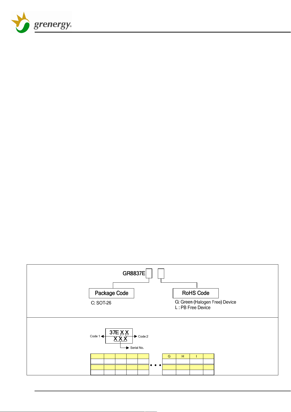
Ordering and Marking Information
SOT-26
65W power converter.
Code 1 8 9 A B
Year 2008 2009 2010 2011
Code 2 1 2 3 4 9 A B C
Month Jan. Feb. Mar. Apr.
Grenergy OPTO Inc. reserves the right to make changes to improve reliability or manufacture ability without notice, and
advise customers to obtain the latest version of relevant information to verify before placing orders.
2012.04 Ver.C.Copyright Grenergy OPTO, Inc. www.grenergy-ic.com
● ● ●
G H I J
2016 2017 2018 2019
Sep. Oct. Nov. Dec.
1
Preliminary GR8837E
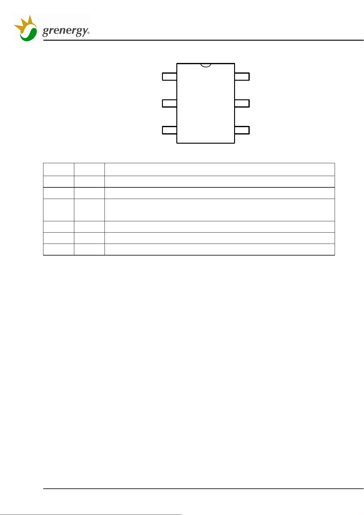
Pin Configuration
GND
1
6
OUT
COMP
2
5
VCC
RTL
3 4
CS
Pin Description
Pin No. Name Function
1 GND Ground pin
2 COMP Voltage feedback pin, by connecting a photo-coupler to control the duty cycle
3 RTL
4 CS Current sense pin, connect to sense the MOSFET current
Resistor trigger latch off which a high over 3.5V for OVP latch off and a low below
1V for OTP latch
5 VCC Power supply pin
6 OUT The output driver for driving the external MOSFET
Absolute Maximum Ratings
Supply voltage VCC --------------------------------------------------------------------------------------------------------- 30V
COMP, RTL, CS ---------------------------------------------------------------------------------------------------- -0.3 ~ 7V
OUT ----------------------------------------------------------------------------------------------------------- -0.3 ~ VCC + 0.3V
Junction temperature ------------------------------------------------------------------------------------------------------- 150℃
Operating ambient temperature ------------------------------------------------------------------------------ -20℃ ~ 85℃
Storage temperature range ---------------------------------------------------------------------------------- -65℃ ~ 150 ℃
SOT-26 package thermal resistance (junction to ambient) -------------------------------------------------- 250℃/W
Power dissipation (SOT-26, at ambient temperature = 85℃) ------------------------------------------------ 250mW
Lead temperature (All Pb free packages, soldering, 10 sec) -------------------------------------------------- 260℃
ESD voltage protection, human body model -------------------------------------------------------------------------- 2KV
ESD voltage protection, machine model ------------------------------------------------------------------------------ 200V
2012.04 Ver.C.Copyright Grenergy OPTO, Inc. www.grenergy-ic.com
2
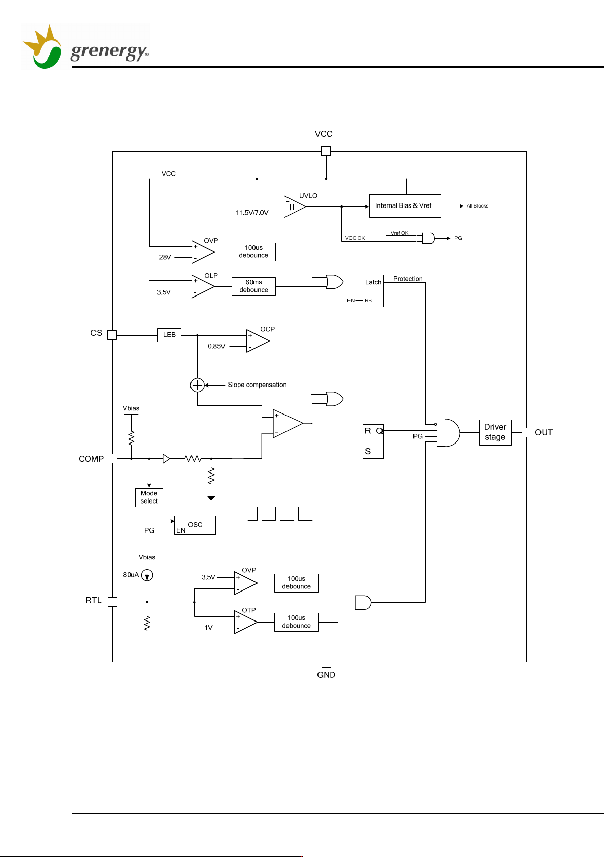
Block Diagram
Preliminary GR8837E
2012.04 Ver.C.Copyright Grenergy OPTO, Inc. www.grenergy-ic.com
3

Preliminary GR8837E
Electrical Characteristics
Parameter Pin
SUPPLY VOLTAGE
Startup Current (VCC=UVLO on - 1V) 5 8 15 uA
Operating Current (with 1nF load on OUT pin), Vcomp = 0V 5 800 uA
Operating Current (with 1nF load on OUT pin), Vcomp = 2.5V 5 1 2 3 mA
Operating Current (with 1nF load on OUT pin), Protection
Tripped (OLP, OVP)
UVLO(off) 5 7.0 V
UVLO(on) 5 11.5 V
OVP Level on VCC Pin-Latch Mode 5 27 28 29 V
VCC Level in Latch Mode (3Meg start-up resistor) 5 6 V
Holding Current at Latch Mode (VCC=5V) 20 uA
Latch Mode Release Voltage 5 3.2 V
VOLTAGE FEEDBACK
Short Circuit Current, Vcomp = 0V 2 0.8 mA
(VCC = 15.0V & TA = +25℃,unless otherwise specified.)
Min. Typ. Max. Unit
5 0.4 0.7 1 mA
Open Loop Voltage, COMP Pin Open 2 4.4 5.5 V
Green-Mode Start Voltage 2 1.5 V
Burst Mode Start Voltage 2 0.85 V
CURRENT SENSING
Maximum Input Voltage, Vcs(off)-Auto Recovery Mode 4 0.80 0.85 0.9 V
Leading-Edge Blanking Time 4 350
Input Impedance 4 1
Delay to Output 4 100 nS
OSCILLATOR
Frequency - 60 65 70 KHz
Jitter Frequency - +6 %
Green Mode Frequency - 22 KHz
Temp. Stability (-40°C ~ 110°C)
Voltage Stability (VCC = 11V~25V) - 3 %
GATE DRIVER OUTPUT
Output Low Level, VCC = 15V, Io = 20mA 6 1 V
- 5 %
nS
MΩ
Output High Level, VCC = 15V, Io = 20mA 6
Rising Time, Load Capacitance = 1000pF 6 150 nS
Falling Time, Load Capacitance = 1000pF 6
VGATE-Clamp (VCC = 25V ) 6 12 13 V
2012.04 Ver.C.Copyright Grenergy OPTO, Inc. www.grenergy-ic.com
8 V
80 nS
4
OLP SECTION
OLP Trip Level, Vcomp (OLP) - 3.5 V
OLP Delay Time - 60 mS
PWM SECTION
Maximum Duty Cycle - 70 75 80 %
RTL SECTION
Over Voltage Protection Threshold Voltage 3 3.2 3.5 3.8 V
OVP Debounce Time 3 100 uS
Over Temperature Protection Threshold Voltage 3 0.95 1 1.05 V
OTP Debounce Time 3 100 us
Output Current from RTL Pin 3 75 80 85 uA
RTL Pin voltage When Floating 3 1.8 2.4 3.0 V
Preliminary GR8837E
2012.04 Ver.C.Copyright Grenergy OPTO, Inc. www.grenergy-ic.com
5
 Loading...