

GREENWICH INSTRUMENTS GR281 User Manual
A
r
GR281 (2K x 8)
M
A7A6A5A4A3A2A1A
A8A
A
A
M
A7A6A5A4A3A2A1A
A8A
A
r
r
r
NON-VOLATILE RA
GR281 (2K x 8)
NON-VOLATILE RA
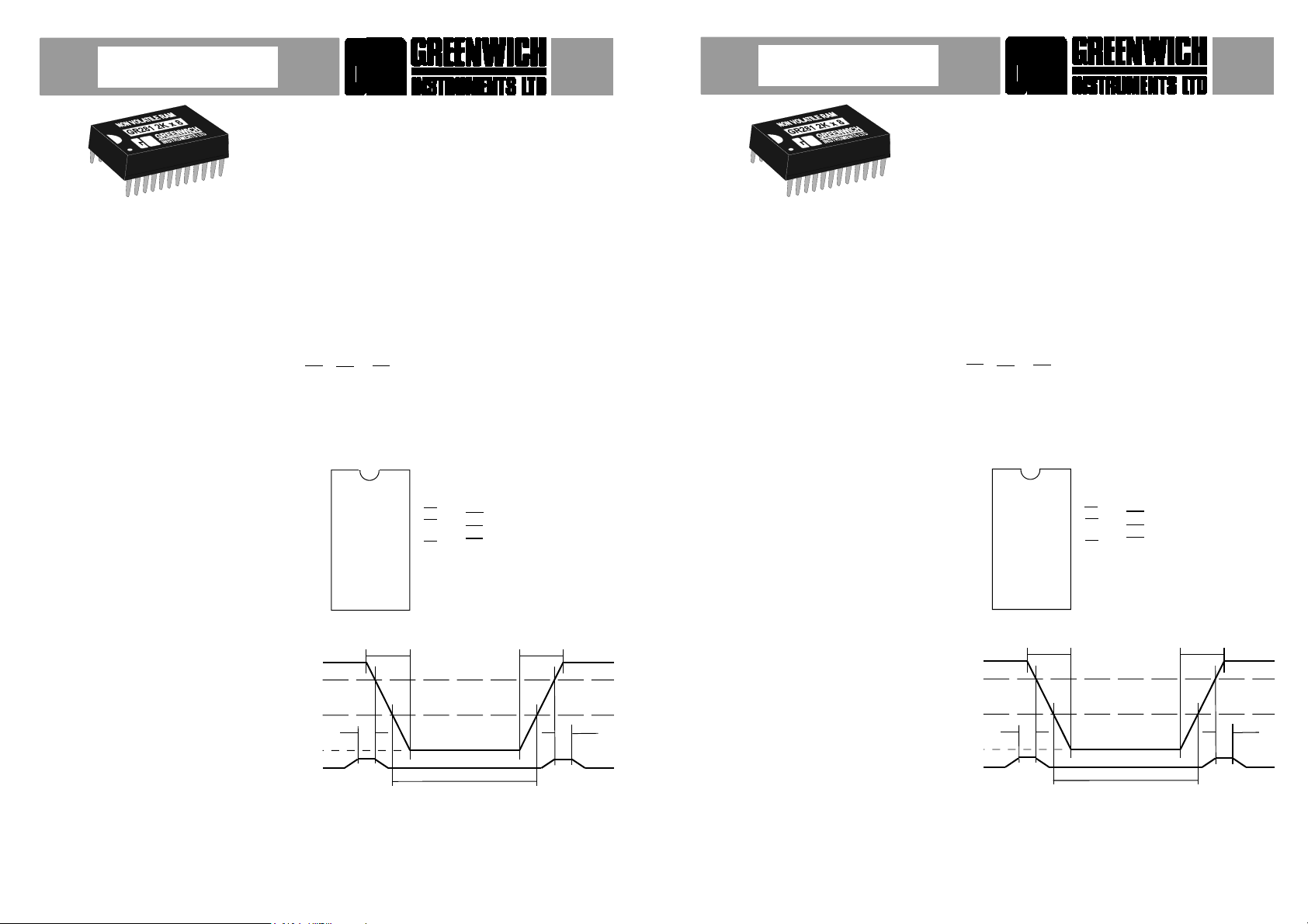
DESCRIPTION
The GR281 is a 2048 word by 8 bits (2K x 8) nonvolatile CMOS Static Ram, fabricated from
advanced silicon gate CMOS technology and a high
reliability lithium power cell.
The pin-out of the GR281 conforms to the JEDEC
standards and is fully compatible with normal static
RAM.
The power down circuit is fully automatic and is
referenced at 4.5 volts. At this point the GR281 is
write protected by an internal inhibit function for Data
Protection and the memory contents are retained by
the lithium power source.
Power down is very fast, this being essential for data
integrity, taking a maximum of 15 µS (15
microseconds) to power down from 5 volts to 0 volts.
This is much faster than system power failure
conditions. Therefore there are no special conditions
required when installing the GR281.
The GR281 can, without external power, retain data
almost indefinitely. The limiting factor will be the
shelf like of the lithium cell, which is typically ten
years. It is possible that this figure may be extended
in view of the extremely light duty imposed upon the
cell.
APPLICATION
When powered down, the GR281 is transportable
and data can be moved from system to system. Being
pin compatible with 2716 EPROM makes it ideal fo
programme development, data collection in data
loggers, programme changes in process control,
automation and robotics and user definable lookup
tables, etc.
DISPOSAL INSTRUCTIONS
Do not dispose of non-volatile memory devices by
incineration or crushing. Devices may be returned
carriage paid to Greenwich Instruments Ltd., fo
disposal.
UK
Greenwich Instruments Ltd.,
Meridian House, Park Road,
Swanley, Kent. BR8 8AH
Tele: 08700 505 404
Fax: 08700 505 405
Symbol Min Max Units
ABSOLUTE MAXIMUM RATINGS
Vdd – 0.3 7.0 Volts
Vi/o – 0.3 Vdd +0.3 Volts
Temp – 20 +70 deg. C
OPERATING CONDITIONS
Symbol Min Typ Max Unit
Vdd 4.75 5.0 5.5 Volts
Vin (1) 2.2 Vdd+0.3 Volts
Vin (0) – 0.3 0.8 Volts
Iin (any other pin) – 1.0 +1.0 µA.
Vout (1)(Iout = –1mA) 2.4 Volts
Vout (0)(Iout = +2mA) 0.4 Volts
Idd (Active) 25 mA.
Idd (Deselected) 1.0 mA.
Tcycle 100 nS.
Cin (any pin) 10 pF
OPERATING MODE
CE OE WR MODE OUTPUT ldd
H X X Unsel. Hi-Z Standby
L H H Unsel. Hi-Z Active
L L H Read Dout Active
L X L Write Din Active
PIN CONNECTIONS
1
2
3
4
5
6
7
8
0
D0
9
D1
10
11
D2
GND
12
DATA RETENTION OPERATING CONDITIONS
Vdd
VTH
3.2V
t
PD
0V
24
Vdd
23
22
9
21
WR
20
OE
19
10
18
CE
17
D7
16
D6
15
D5
14
D4
13
D3
t
F
>
<
>
<
<
PIN DESIGNATIONS
Pin Function
0-A10 Address I/P`s
D0-D7 Data in/out
OE Output Enable
CE Chip Enable
WR Write Input
Vdd +5Volt Power
GND Ground
t
R
<
>
t
DR
>
>
t
REC
<
Symbol Parameter Min Typ Max Units
Vdd Operating supply voltage 4.75 5.0 5.50 Volts
VTH Data retention voltage 4.5 Volts
t
F Vdd slew to 0V 15 µS
t
R Vdd slew 0V to 5.0V 15 µS
t
REC CE to O/P valid from power up 15 µS
t
DR Data retention time 10 Years
t
PD CE at Vin(1) before power down 0 µS
DESCRIPTION
The GR281 is a 2048 word by 8 bits (2K x 8) nonvolatile CMOS Static Ram, fabricated from
advanced silicon gate CMOS technology and a high
reliability lithium power cell.
The pin-out of the GR281 conforms to the JEDEC
standards and is fully compatible with normal static
RAM.
The power down circuit is fully automatic and is
referenced at 4.5 volts. At this point the GR281 is
write protected by an internal inhibit function for Data
Protection and the memory contents are retained by
the lithium power source.
Power down is very fast, this being essential for data
integrity, taking a maximum of 15 µS (15
microseconds) to power down from 5 volts to 0 volts.
This is much faster than system power failure
conditions. Therefore there are no special conditions
required when installing the GR281.
The GR281 can, without external power, retain data
almost indefinitely. The limiting factor will be the
shelf like of the lithium cell, which is typically ten
years. It is possible that this figure may be extended
in view of the extremely light duty imposed upon the
cell.
APPLICATION
When powered down, the GR281 is transportable
and data can be moved from system to system. Being
pin compatible with 2716 EPROM makes it ideal fo
programme development, data collection in data
loggers, programme changes in process control,
automation and robotics and user definable lookup
tables, etc.
DISPOSAL INSTRUCTIONS
Do not dispose of non-volatile memory devices by
incineration or crushing. Devices may be returned
carriage paid to Greenwich Instruments Ltd., fo
disposal.
UK
Greenwich Instruments Ltd.,
Meridian House, Park Road,
Swanley, Kent. BR8 8AH
Tele: 08700 505 404
Fax: 08700 505 405
Symbol Min Max Units
ABSOLUTE MAXIMUM RATINGS
Vdd – 0.3 7.0 Volts
Vi/o – 0.3 Vdd +0.3 Volts
Temp – 20 +70 deg. C
OPERATING CONDITIONS
Symbol Min Typ Max Unit
Vdd 4.75 5.0 5.5 Volts
Vin (1) 2.2 Vdd+0.3 Volts
Vin (0) – 0.3 0.8 Volts
Iin (any other pin) – 1.0 +1.0 µA.
Vout (1)(Iout = –1mA) 2.4 Volts
Vout (0)(Iout = +2mA) 0.4 Volts
Idd (Active) 25 mA.
Idd (Deselected) 1.0 mA.
Tcycle 100 nS.
Cin (any pin) 10 pF
OPERATING MODE
CE OE WR MODE OUTPUT ldd
H X X Unsel. Hi-Z Standby
L H H Unsel. Hi-Z Active
L L H Read Dout Active
L X L Write Din Active
PIN CONNECTIONS
0
D0
D1
D2
GND
DATA RETENTION OPERATING CONDITIONS
Vdd
VTH
3.2V
t
0V
1
2
3
4
5
6
7
8
9
10
11
12
PD
24
Vdd
23
22
9
21
WR
20
OE
19
10
18
CE
17
D7
16
D6
15
D5
14
D4
13
D3
t
F
>
<
>
<
<
PIN DESIGNATIONS
Pin Function
0-A10 Address I/P`s
D0-D7 Data in/out
OE Output Enable
CE Chip Enable
WR Write Input
Vdd +5Volt Power
GND Ground
t
R
<
>
t
DR
>
>
<
Symbol Parameter Min Typ Max Units
Vdd Operating supply voltage 4.75 5.0 5.50 Volts
VTH Data retention voltage 4.5 Volts
t
F Vdd slew to 0V 15 µS
t
R Vdd slew 0V to 5.0V 15 µS
t
REC CE to O/P valid from power up 15 µS
t
DR Data retention time 10 Years
t
PD CE at Vin(1) before power down 0 µS
t
REC
A
A
A
GR281 (2K x 8)
M
A
A
A
A
A
A
A
A
M
A
A
A
A
A
NON-VOLATILE RA
GR281 (2K x 8)
NON-VOLATILE RA
ddress
D
OUT
ddress
D
D
ddress
D
D
CE
OE
CE
WE
OUT
IN
CE
WE
OUT
IN
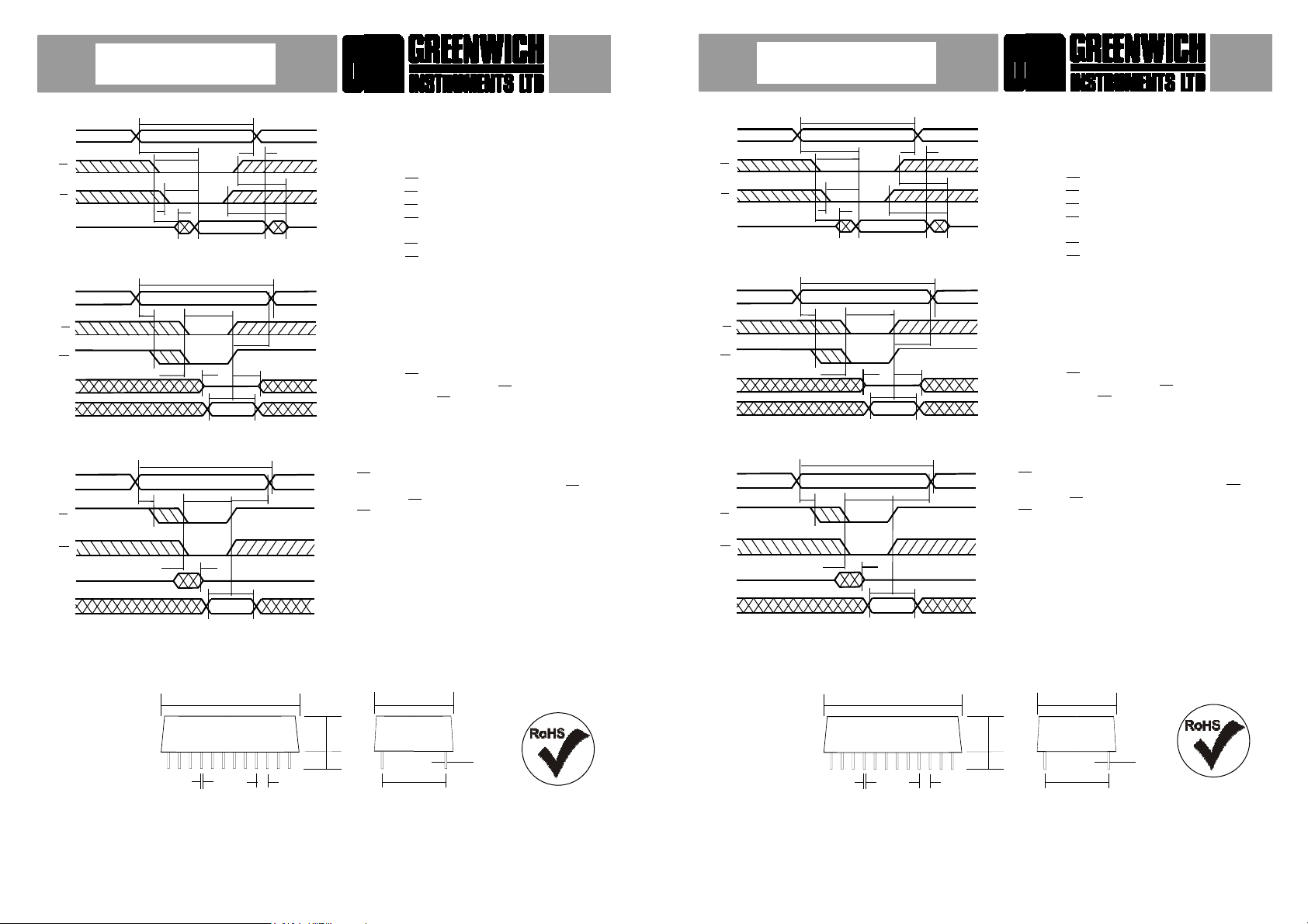
READ CYCLE
t
<
<
WRITE CYCLE 1
<
t
<
<
t
<
RC
t
ACC
>
t
ACS
<
>
t
OE
<
>
t
OLZ
>
<
t
CLZ
<
>
t
WC
S
>
S
>
t
WP
<
t
WHZ OW
>
<<
WRITE CYCLE 2
t
WC
t
WP
<
t
WHZ
<
>
t
DS
<
t
DS
<<>>
TIMING (nS-nano seconds)
>
t
OH
<
>
t
CHZ
<
>
t
OHZ
<
>
<
<
<
>
>
>
t
WR
>
t
>
t
DH
>>
>
t
WR
>
t
DH
Read Cycle 100nS
Symbol Parameter Min Max
t
RC Read cycle time 100
t
CC Access time 100
t
CS CE to output valid 100
t
OE OE to output valid 40
t
CLZ CE to output active 10
t
OLZ OE to output active 10
t
OH Output hold time 10
t
CHZ CE to output disable 40
t
OHZ OE to output disable 40
Write Cycle 100nS
Symbol Parameter Min Max
t
WC Write cycle time 100
t
WP Write pulse width 60
t
S Address setup time 0
t
WR Write recovery time 10
t
WHZ WR to output disable 30
t
OW Output active from WR 10
t
DS Data setup time 30
t
DH Data HOLD TIME 10
Notes
1. WE must be high during address transitions.
2. A Write occurs during the overlap of active CE
and a low WE.
3. WE is high for a read cycle.
REPLACES
2016., 6116., 8416., 5517., 4016., 2128., 5128.,
PD446., 8128., 4802., 5116., etc.
ddress
D
OUT
ddress
D
D
ddress
D
D
CE
OE
CE
WE
OUT
IN
CE
WE
OUT
IN
READ CYCLE
t
RC
t
ACC
<
WRITE CYCLE 1
<
t
<
<
t
<
>
t
ACS
<
>
t
OE
<
>
t
OLZ
>
<
t
CLZ
<
>
t
WC
S
>
S
>
t
WP
<
t
WHZ OW
<
>
WRITE CYCLE 2
t
WC
t
WP
t
WHZ
<
>
><
t
OH
<
>
t
CHZ
<
>
t
OHZ
<
>
>
Read Cycle 100nS
Symbol Parameter Min Max
t
RC Read cycle time 100
t
CC Access time 100
t
CS CE to output valid 100
t
OE OE to output valid 40
t
CLZ CE to output active 10
t
OLZ OE to output active 10
t
OH Output hold time 10
t
CHZ CE to output disable 40
t
OHZ OE to output disable 40
Write Cycle 100nS
>
t
WR
>
<
t
>
<
t
t
DS
DH
<
<
>
>
>
Symbol Parameter Min Max
t
WC Write cycle time 100
t
WP Write pulse width 60
t
S Address setup time 0
t
WR Write recovery time 10
t
WHZ WR to output disable 30
t
OW Output active from WR 10
t
DS Data setup time 30
t
DH Data HOLD TIME 10
Notes
1. WE must be high during address transitions.
t
WR
>
<<
>
2. A Write occurs during the overlap of active CE
and a low WE.
3. WE is high for a read cycle.
t
t
DS
DH
<
<>>
REPLACES
2016., 6116., 8416., 5517., 4016., 2128., 5128.,
PD446., 8128., 4802., 5116., etc.
TIMING (nS-nano seconds)
DIMENSIONS (mm)
<
Greenwich Instruments Ltd., are continually developing their products and reserve the right
to alter specifications without prior notice. Standard Terms and Conditions of Sale apply.
32
<
>
>
>
7.3
>
4
>>
2.50.5
<>
18
<
0.38
<>>
15.24
<
>
2000/95/EC
<
<
>
Greenwich Instruments Ltd., are continually developing their products and reserve the right
to alter specifications without prior notice. Standard Terms and Conditions of Sale apply.
http://www.greenwichinst.co.uk
ISSUE 4 OCT 2005
DIMENSIONS (mm)
32
>
>
>
2.50.5
<>
<
>
7.3
>
4
<
http://www.greenwichinst.co.uk
18
15.24
0.38
<>>
>
2000/95/EC
ISSUE 4 OCT 2005
 Loading...