

Page 1

Page 2
Page 3
Page 4
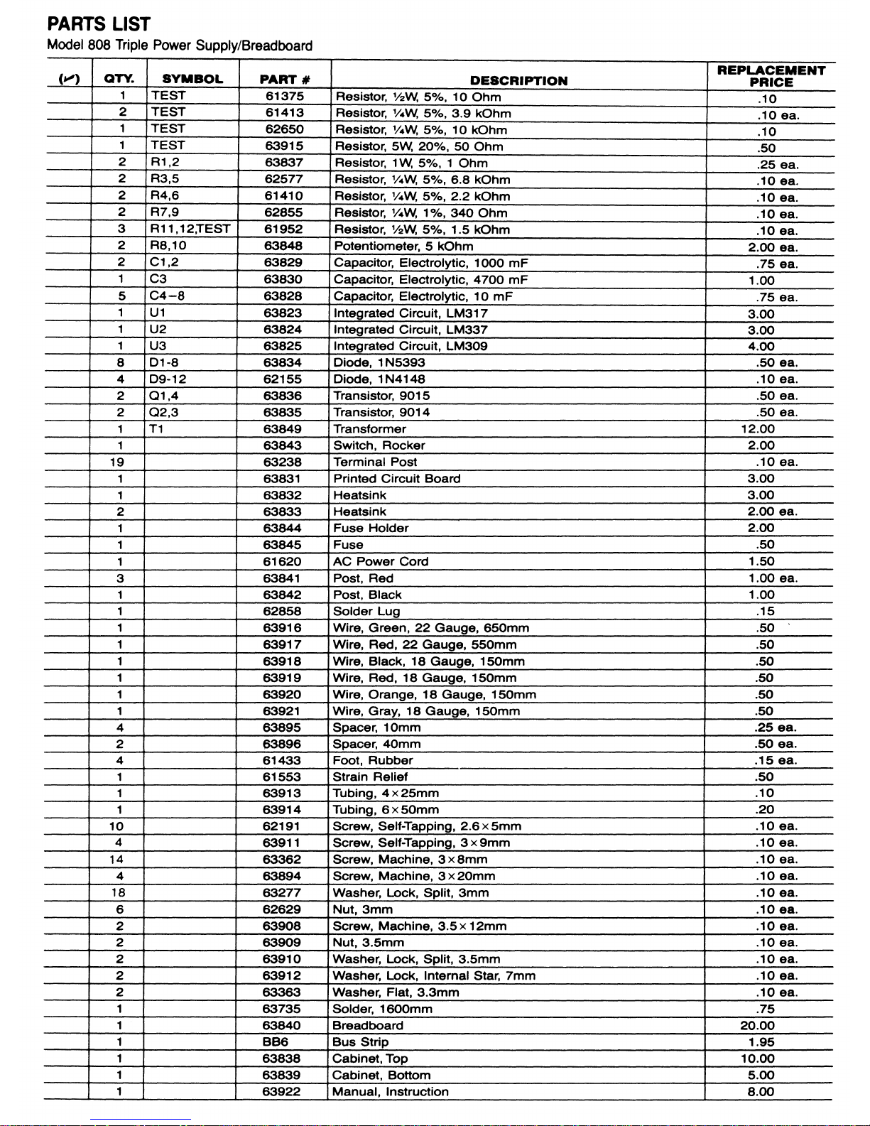
Page 5

PARTS IDENTIFICATION AND INVENTORY EXPERIENCE
This experience is provided to acquaint you with the
ous electronic components and fittings included in this
To assist you in proper identification of the major parts and
project. Unpack the project carefully and check
each
fittings, pictorial and schematic illustrations are given in
part and fitting against the PARTS LIST In case of incor-
Figure
rect, missing, or damaged parts, please refer to How to
der Replacement Parts and Graymark’s Warranty.
Upon completion of the parts identification and inventory,
have your instructor initial your Progress Guide.
DIODE, SIGNAL
INTEGRATED CIRCUIT
FUSE HOLDER
DIODE, POWER
TRANSFORMER
POWER RESISTOR
HEAT SINK
POST, RED,
POTENTIOMETER
RUBBER FOOT
SOLDER LUG
MACHINE SCREW
SELF-TAPPING SCREWS
AND 2.6 x
SPACER
AND
ELECTROLYTIC
CAPACITOR
PCB
BREADBOARD
--
__.
LOCK WASHER SPLIT
STRAIN RELIEF
AND INTERNAL STAR
TRANSISTOR
1
5
Page 6
Page 7
Page 8
Page 9
Page 10

Page 11
Page 12
Page 13
Page 14
Page 15
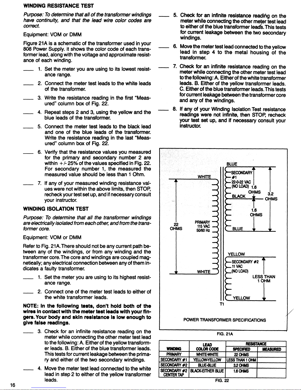
Page 16
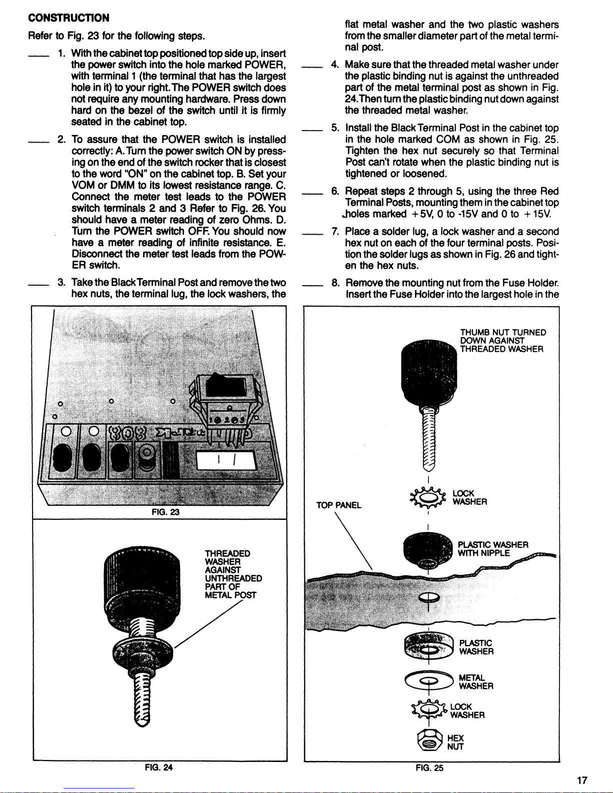
Page 17
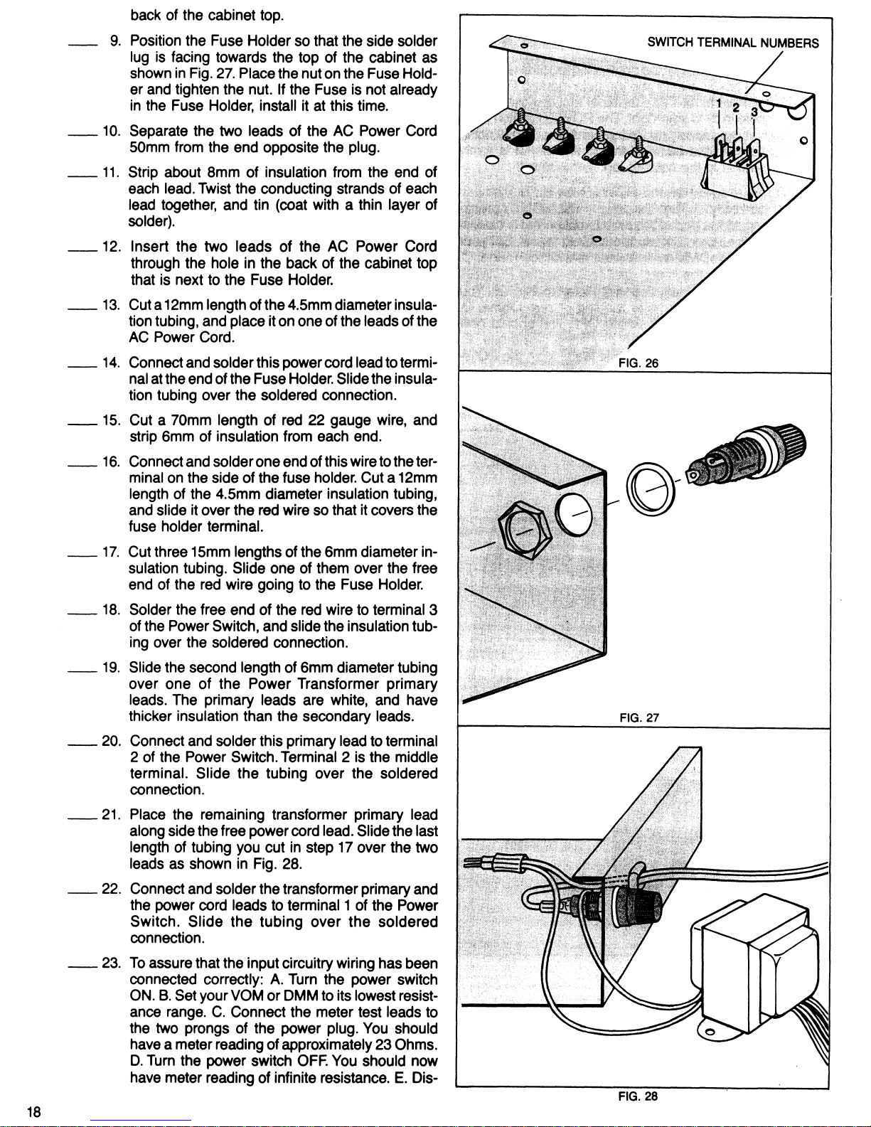
Page 18
Page 19
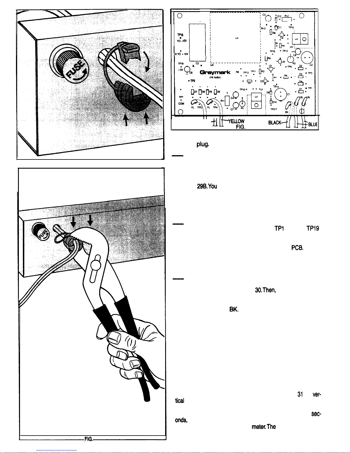
FIG. 29A
29B
l
0
5”
TP17
, RlO
r----------
i
l
, .
l Tm
. . . .
YELLOW
30
connect the meter test leads from the power
24. Position the two portions of the AC power cord
grommet around the cord where it extends out of
rear of the cabinet top, as shown in Fig. 29A. Using slip-joint pliers, insert the grommet into the
hole in the rear of the cabinet top as shown in Fig.
will have to squeeze the grommet quite
hard with the pliers so that the power cord is
formed into a “U” inside the grommet, and the
grommet is compressed enough to fit into the
hole.
25. Locate the Printed Circuit Board (PCB) and the
test points. Insert and solder
through
into the PCB. The test points are inserted from
the component side of the PCB and soldered to
the copper on the solder side of the
Refer
to Fig. 30 and the the silkscreened legend on the
component side of the PCB for the test point
locations.
26.
From the solder side (bottom) of the PCB thread
the transformer leads through the holes in the
PCB as shown in Fig.
from the component side (top) of the PCB, thread the stripped
and tinned wire ends through the holes marked
YL, BL and
Solder these five wires to the
PCB, and cut off any excess lead length. Note:
This is done so when the board is handled during
component installation and testing, the wires
won’t bend and break at the weak points where
the wire insulation stops and the tinned copper
wire goes through the PCB.
AC VOLTAGE WAVEFORMS AND VALUES
DISCUSSION
Measuring a DC voltage is simple and straight forward.
Shown on a graph, the voltage of an automobile battery
would appear as a straight horizontal line. In Fig.
the
axis shows the magnitude of the voltage being meas-
ured, and the horizontal axis represents time. The time
shown on the graph would be in the order of several
the time it takes for the meter pointer to stabilize and
for you to accurately read the
graph shows that
the meter test probes were connected to the the battery at
19
Page 20
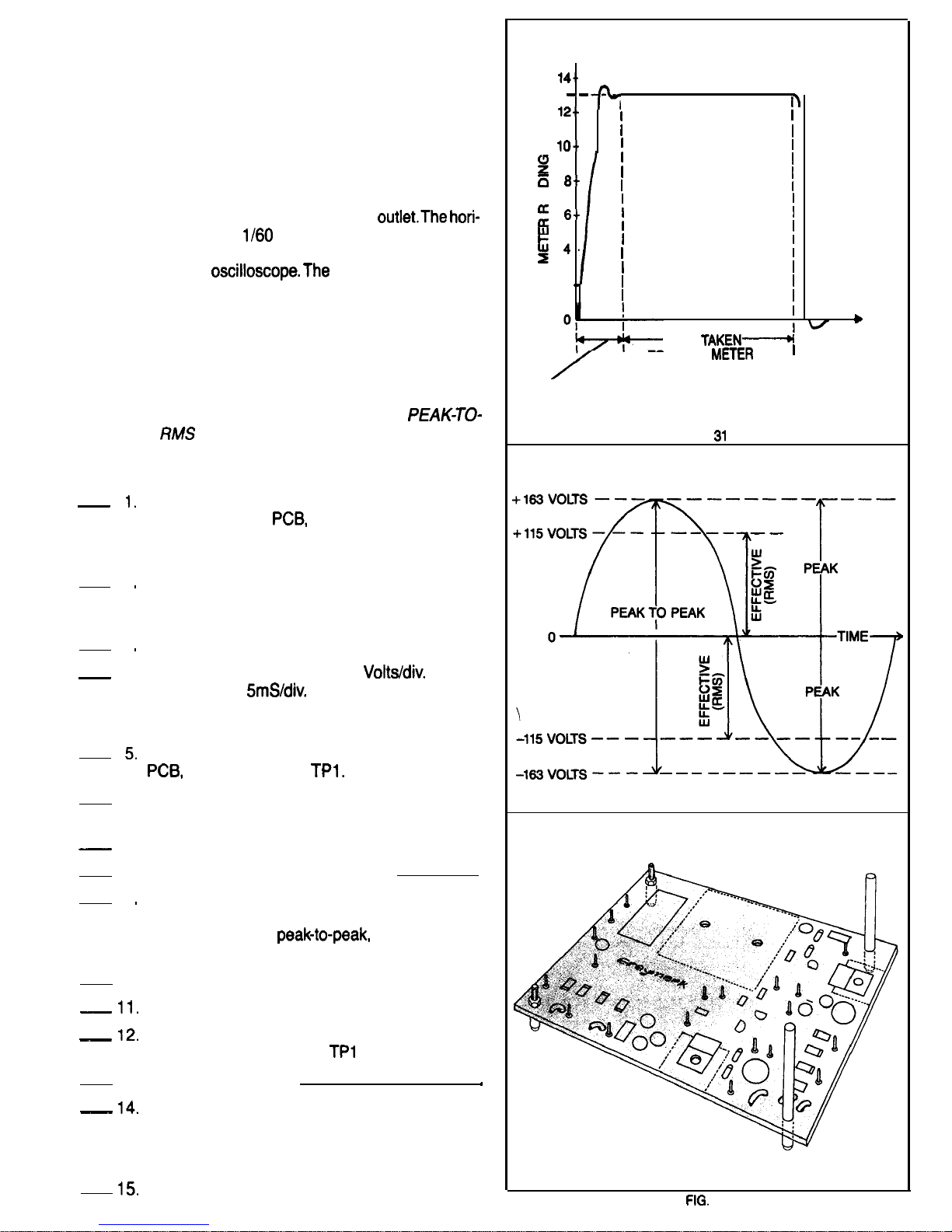
time (T) 0, and removed immediately after the meter was
read.
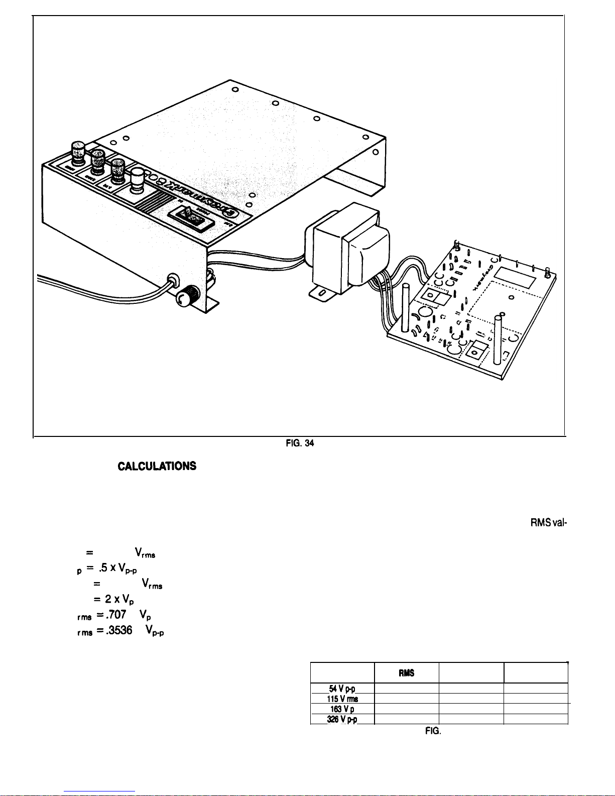
To show an AC voltage, we need to change our graph in
two ways. It will have to indicate voltages of both polarities,
positive and negative, and we will have to make the horizontal axis cover a much smaller period of time.The public
utility companies in the United States provide 60 Hertz
power. Hertz, abbreviated Hz, means cycles per second.
60 Hz means that the polarity of the voltage is reversing
120 times a second.
Figure 32 is a graph of the voltage at a wall outlet.The
zontal axis only covers
of a second of time, or 16.67
milliseconds (mS).To observe what this graph shows, you
will have to use an
AC voltage ranges of
a VOM will indicate the rms voltage, but the meter cannot
respond to the rapid changes of the 60 Hz. AC voltage, and
even if it could your eye could not read
meter pointer.
AC VOLTAGE OBSERVATION and
EXPERIENCE
Purpose: To observe and measure
PEAK, and
Voltages.
Equipment: OSCILLOSCOPE
VOM or DMM
the rapidly moving
MEASUREMENT
PEAK,
2
3
4.
6
.
7.
8
.
9
IO.
13.
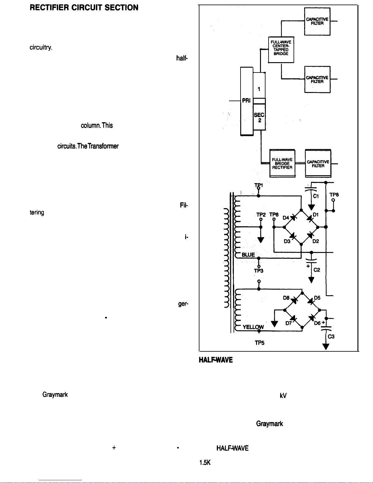
Refer to Fig. 33. Mount the 1 Omm spacers on the
solder side of the
using the four 20 x 3mm
machine screws, the two 40mm spacers, and
two 3mm nuts.
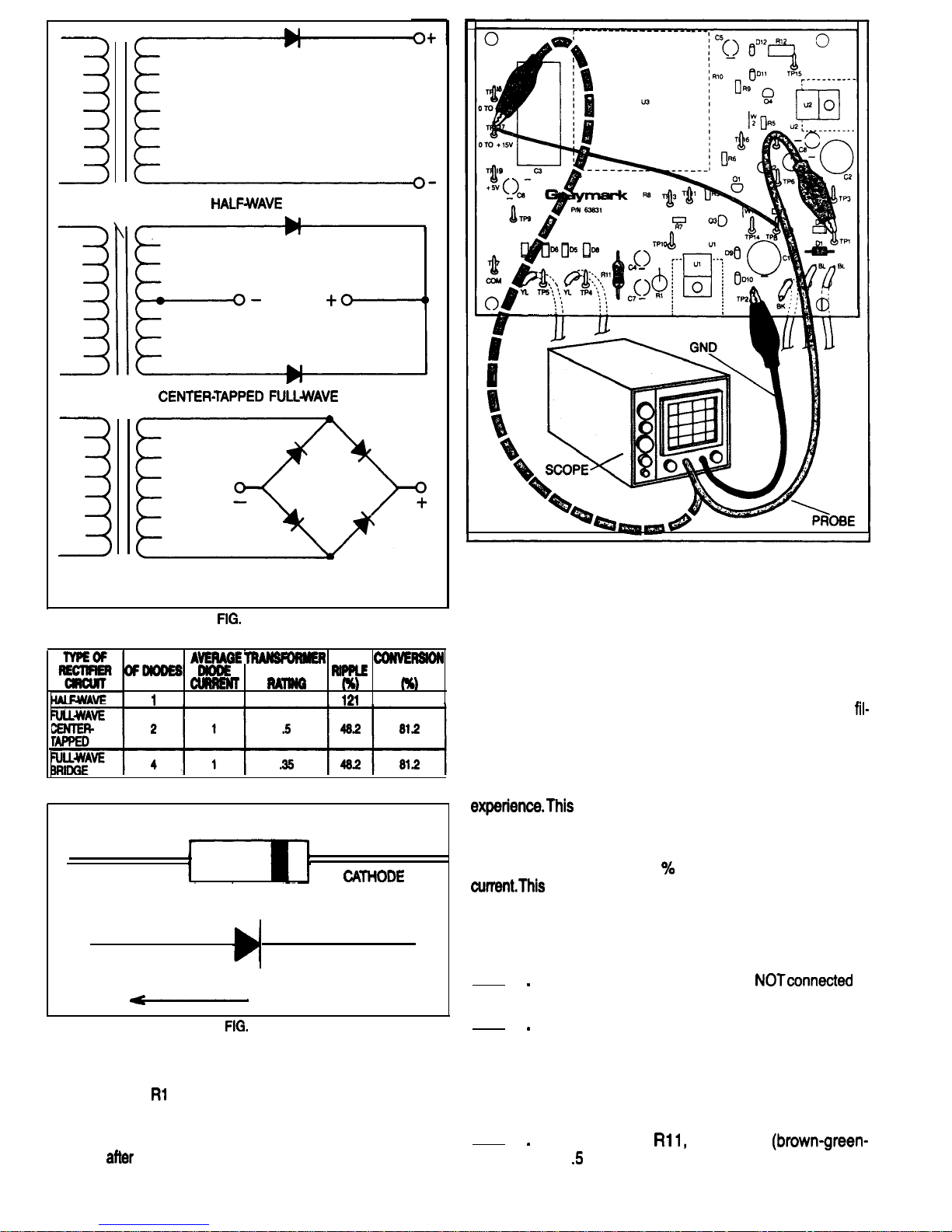
Place the cabinet top assembly, the power transformer and the PCB on a work surface as shown
in Fig. 34.
Set the oscilloscope power switch to On.
Adjust the Oscilloscope to 10
Set the
sweep rate to
Adjust the input controls
to display an AC signal, and vertical positioning
at the CENTER line.
Connect the scope ground lead to TP2 of the
and the probe to
Connect the power plug of the 808 to a 115 VAC
power outlet.
Set the power switch to ON.
Record your peak-to-peak reading
l
If your reading is about 60 Volts peak to peak,
then proceed to the next step. If your reading is
not about 60 Volts
stop, and check
your test set up or consult your instructor.
Remove the scope probe.
Adjust the VOM or DMM to read 19 Volts AC.
Connect one meter test lead toTP2 of the PCB,
and the other test lead to
.
Record your reading
If your reading is about 21 Volts AC, proceed to
the next step. If your reading is not about 21 Volts
AC, then stop and check your test set up or con-
sult your instructor.
Remove the test leads.
13.0
VOLTS-
&-
i3
2
TIME
TIME
TO READ
TIME FOR
METER TO
STABILIZE
FIG.
FIG. 32
33
20
Page 21
MATHEMATICAL
AND DEFINITIONS
Purpose: To demonstrate that the previous experience is
in agreement with the mathematical formulas
The following formulas are used to calculate ROOT MEAN
SQUARE, PEAK and PEAK-to-PEAK AC sine wave Voltages, Refer to Fig. 32.
VP 1.414 x
V
x
V
P-P
2.828 x
V
P-P
V
x vp
V
x
PEAK VALUE (p): The amplitude of a voltage measured
from zero or reference axis to its maximum value, when the
voltage alternates between positive and negative half
cycles.
PEAK-to-PEAK (p-p): The amplitude of a voltage meas-
ured from maximum positive peak to maximum negative
peak, when the voltage alternates between positive and
negative half cycles.
ROOT MEAN SQUARE (RMS): The effective or RMS val-
ue of a voltage is the SQUARE ROOT of the average
(MEAN) of the squares of all the instantaneous values of
the voltage over one cycle. For a sine voltage, the
ue is equal to 0.707 times the maximum peak value of the
voltage.
INSTANTANEOUS VALUE: The exact value of the amplitude of a voltage at a particular instant in time.
Using the above formulas, calculate the unknown voltages
in Fig. 35.
This completes the AC VOLTAGE OBSERVATION and
MEASUREMENT EXPERIENCE.
Have your instructor
initial your progress guide.
MEASURED
VALUE
PEAK-TO-PEAK
PEAK
,
.
35
71
Page 22
DISCUSSION
Figure 36 is a partial block diagram and schematic of the
808 Power Supply, showing the rectifiers and associated
There are three basic types of rectifier circuits: the
wave, the full-wave center-tapped, and the full-wave
bridge. Each of these rectifier circuits uses a different number of diodes and requires a transformer winding with a different rating. Figures 36A and 37 identify some of the differences between these three types of circuits.
The first column in Fig. 37 contains the three types of rectifier circuits. The number of diodes used by each circuit is
listed in the second column. The average diode current is
shown in the third
value has significance because diodes with a higher current rating are required for
half-wave circuits, as compared to those required by the
other two
Power Rating column is
also important, since each type of circuit requires a transformer or a transformer winding with a different power capacity. And, the larger the power capacity required, the
greater the size and the cost of the transformer.
The Ripple column refers to the percentage of ac voltage
contained in the DC output of the rectifier circuit. A decrease in the percentage of ripple offers a corresponding
decrease in the amount of capacitance required in the
Stage. Since lower value capacitors are smaller in
size and cost less, a low percentage of ripple from the rectifier circuit is desirable.
Finally, the Conversion Efficiency column indicates the eff
ciency of each Rectifier Circuit in converting alternating
current to direct current. Notice that the full-wave rectifier
circuits are twice as efficient as the half wave circuit.
The heart of the rectifier circuit is the diode. Most diodes
are made from silicon or germanium, both of which are
semiconductors. Silicon is used for almost all diodes used
in power supply rectifier circuits, as it is capable of operat-
ing a higher temperature than germanium. For a given size
of device, a silicon diode can pass more current than a
manium diode. A diode is a component which will allow cur-
rent to flow in one direction
from cathode to anode. Refer
to Fig. 38.
Alternating current flows first in one direction, then the op-
posite direction, then reverses direction again. This alter-
nating action occurs continuously. Direct current, on the
other hand, flows in only one direction. A diode can be put
in the path of an alternating current to block the current flow
in one direction and permit the current flow in the opposite
direction. It is in this manner that alternating current is recti-
fied or converted into pulsating direct current.
The
Model 808 Power Supply uses four silicon
diodes in a full-wave bridge rectifier circuit, and four more
silicon diodes in a center-tapped full-wave bridge
rectifier circuit.
The center-tapped full-wave rectifier circuit combines features of the center-tapped full-wave and the full-wave
bridge rectifier circuits. It is used in the 808 Power Supply
to provide power for the 0 to
15 Volt and the 0 to
15
Volt outputs. Before going on to the FILTERING section,
you will build and test four types of rectifier circuits.
POWER
TRANSFORMER
SEC
.
RECTIFIER
BLUE
TP4
Tl
A
FIG. 36
RECTIFIERS
DISCUSSION
Half-wave rectifier circuits are sometimes used where the
current requirements are low, in the order of 10 to 100
microamps, and voltages of 1
(1000 Volts) or higher are
needed. Photomultiplier tubes and Ion chambers, which
are used to detect and measure radiation, are examples of
devices requiring this type of DC power. Utility power supplies, such as your
808, which are generally
used to power solid state analog and digital devices, do
not usually use half-wave rectifier circuits.
In the
RECTIFIER TEST, you will be viewing
the output of a half-wave rectifier on an oscilloscope. A
Ohm resistor (Rl 1) is connected across the output of
22
Page 23
Without it, dangerously high voltages could remain present
FULL WAVE BRIDGE
long after the input power has been turned off or
TYPES OF RECTIFIER CIRCUITS
disconnected.
36A
SIGNIFICANT RECTIFIER CIRCUIT CHARACTERISTICS
NUMBER
POWER
EFFICIENCY
REQUIRED
,
2
1
4Q.6
FIG. 37
DIODE
ANODE CATtiODE
ANODE
CATHODE
CURRENT FLOW
36
the rectifier circuitry. Figure 43 is a schematic of this circuit.
Without this resistor, stray circuit capacitances could distort
the waveform displayed on the scope. In the completed
Power Supply
1 serves as a bleeder resistor.
One of the functions of a bleeder resistor is to discharge
or “bleed off” the electrical energy remaining in the filter capacitors
the power supply is turned off. In high voltage
supplies, the bleeder resistor is an important safety device.
FIG. 39
The output voltages of the Model 808 Triple Power Supply
are not high enough to be hazardous to the person using
it, but it is disconcerting when a power supply that has been
turned off earlier generates a spark if an output is acciden-
tally shorted. In the 808 Power Supply, bleeder resistors,
along with the voltage regulators, serve to discharge the
ter capacitors within seconds after the input power has
been switched off or disconnected.
When you are building your 808, you will be instructed to
install some components long before they are used in an
is to provide a discharge path for the filter
capacitors before the voltage regulators are installed.
In unregulated power supplies the bleeder resistor is is
often designed to draw 10
or more of the rated output
is to improve the voltage regulation of the sup-
ply under changing load conditions.
CONSTRUCTION
Refer to Fig. 39 for the following steps.
1
2
3
Be sure the 808 power plug is
to
a power outlet.
Mount diode Dl on the PCB. Be sure that the
banded end of the diode is oriented the same as
the diode outline that is silkscreened on the PCB.
Using a heat sink as shown in Fig. 40, solder the
diode leads to the PCB. cut off any excess lead
length.
Mount resistor
1 SK Ohm
red)
Watt, on the PCB. Solder the leads to the
PCB and cut off any excess length.
23
Page 24
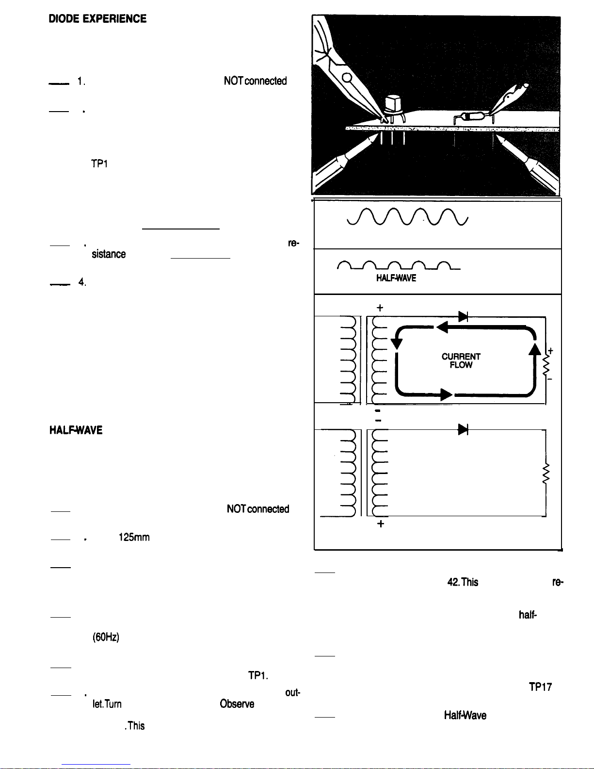
Purpose: To observe the current blocking capability of a
diode.
Equipment: VOM or DMM
2
3
Be sure the 808 power plug is
to
a power outlet.
Set the meter you are using to its lowest ohmme-
ter range. If your meter has an range marked with
a diode symbol or the word “diode”, use that
range instead. Connect the positive* meter test
lead to TP8 and the negative* meter test lead to
, (If your uncertain what the asterisks after
the words “positive” and “negative” mean, review
the last paragraph of the section titled USING AN
OHMMETER ON POLARIZED CIRCUITS AND
CIRCUITRY) Record the resistance reading.
Reverse the meter test leads and record the
reading.
Disconnect the
meter test leads from the test points.
In the 2nd step, you should have had an infinite
resistance reading, indicating that the direct current from the ohmmeter was being blocked. In
the 3rd step, there should have been a much low-
er resistance reading, indicating that the current
was passing through the diode. This illustrates
the ability of a diode to permit current to flow in
one direction, and to restrict its flow in the opposite direction. The difference between the two
conditions depends upon the polarity of the voltage applied to the diode. The anode of a diode
has to be at a more positive potential than the
cathode for current to flow to occur.
RECTIFIER EXPERIENCE
Purpose: To observe the voltage waveform produced by a
Half-Wave Rectifier circuit.
Equipment: Oscilloscope
Refer to Fig. 39 for the following steps.
1.
2
3
l
4.
5
l
6
Be sure the 808 power plug is
to
a power outlet.
Cut a
length of red 22 gauge wire, and
strip 6mm of insulation from each end.
Solder one end of the red wire to TP8, and the
other end toTP17. Because these are temporary
connections for testing purposes, its not necessary to make mechanical connections.
Turn the oscilloscope ON and let it warm up. Ad-
just it to display a 60 Volt (peak to peak) 60 Hertz
signal. Set the vertical (Y) input coupling
to DC.
Connect the oscilloscope (scope) ground lead to
TP2, and the scope input probe to
Plug the 808 Power Supply plug into a power
the power switch ON.
the wave-
form displayed on the scope. It should look like
Fig. 41
is ac voltage which is present at the
secondary winding of the transformer.
TRANSFORMER
SECONDARY
AC VOLTAGE
FIG. 41
CATHODE OF Dl
RECTIFICATION
FIG. 42
l
NO
CURRENT
FLOW
HALF WAVE RECTIFIER CIRCUIT
L
FIG. 43
7. Move the scope probe to TP17. The waveform
should look like Fig.
waveform is the
sult of diode Dl rectifying the ac voltage. Dl clips
off the negative half of the waveform, leaving
only the positive half. This is called
wave
rectification. Current flow in a half-wave rectifier
circuit is illustrated in Fig. 43.
8. Turn the 808 Power switch Off and disconnect
the power plug from the outlet. Disconnect the
scope common lead and input Probe. Leave the
red wire that is soldered to TP8 and
in
place.
9. This completes the
Rectifier Experience. Have your instructor initial your Progress
Guide.
24
Page 25
CENTER-TAPPED RECTIFIERS
DISCUSSION
A
center-tapped rectifier circuit requires a transformer with a secondary winding which has a tap halfway
between both ends of the winding (a center-tap). secondary
number 2 of the 808 Power Supply transformer is a
tapped winding. You have already used one half of this
winding in the
Rectifier section.
CENTER-TAPPED
RECTIFIER EXPERIENCE
To observe the voltage waveform produced by a
Rectifier circuit.
Equipment: Oscilloscope
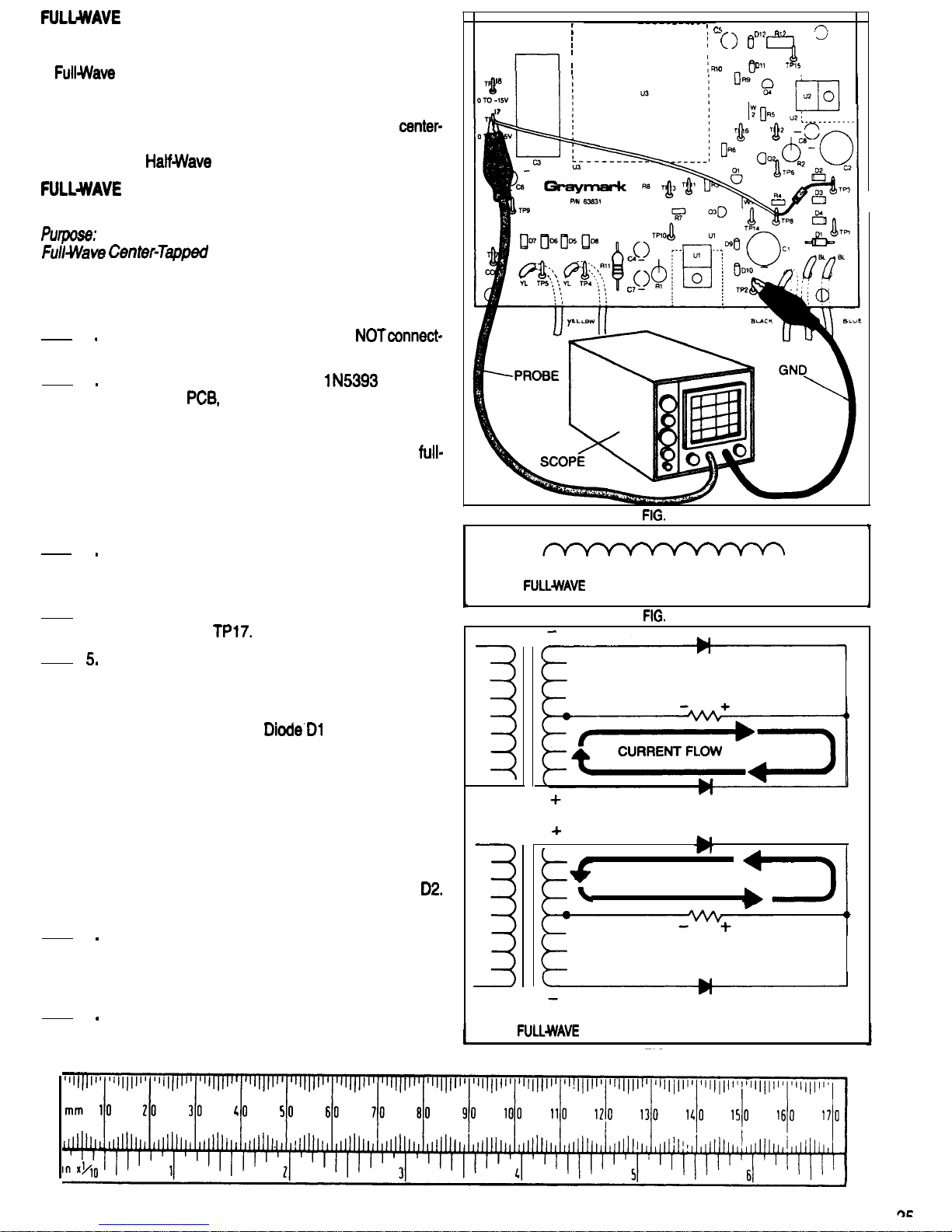
Refer to Fig. 44 for the following steps.
12Be sure that the 808 power plug is
ed to a power outlet.
3
4
l
Solder the cathode lead of a
diode to
TP8 of the
and the anode lead toTP3. Do
not cut the diode leads, or remove the red wire
soldered to TP8. This is a temporary installation
of D2. This diode will be removed after the
wave filter test and installed later in its permanent
location. Since the long leads isolate the heat of
soldering from the diode itself, it is not necessary
to use a heat sink.
Turn the scope ON and let it warm up. Adjust it
to display a 60 Volt (peak to peak) 60 Hz signal.
Set the vertical input (Y) coupling to DC.
Connect the scope ground lead toTP2, and the
45
input probe to
Connect the 808 Power Supply plug to a power
outlet. Turn the power switch ON. The waveform
displayed on the scope should look like Fig. 45.
Both halves of the ac cycle are now being rectified. Refer to Fig. 46.
rectifies the current from one half of the secondary winding, and
diode D2 rectifies the current from the other half
of the winding. Since the diode cathodes are
connected together, both their waveforms are
joined together to produce a composite waveform. This composite waveform is composed of
two sets of positive voltage half cycles. One set
is from Dl ,and the other set, which is 180 degrees out of phase with the first set, is from
This is called full-wave rectification.
6
Turn the 808 Power switch OFF and disconnect
the power plug from the outlet. Disconnect the
scope common lead and input probe. Leave diode D2 and the red wire in place.
7
This completes the Full-Wave Center-Tapped
0
I--
l
r---------
44
RECTIFICATION, POSITIVE OUTPUT
NO CURRENT FLOW
CURRENT FLOW
NO CURRENT FLOW
CENTER-TAPPED RECTIFIER CIRCUIT
Rectifier Test. Have your instructor initial your
Progress Guide.
FIG. 46
Page 26
bridge rectifiers are used in a wide range of pow-
er
rectifier circuits are among the most effi-
cient and cost effective for many applications.
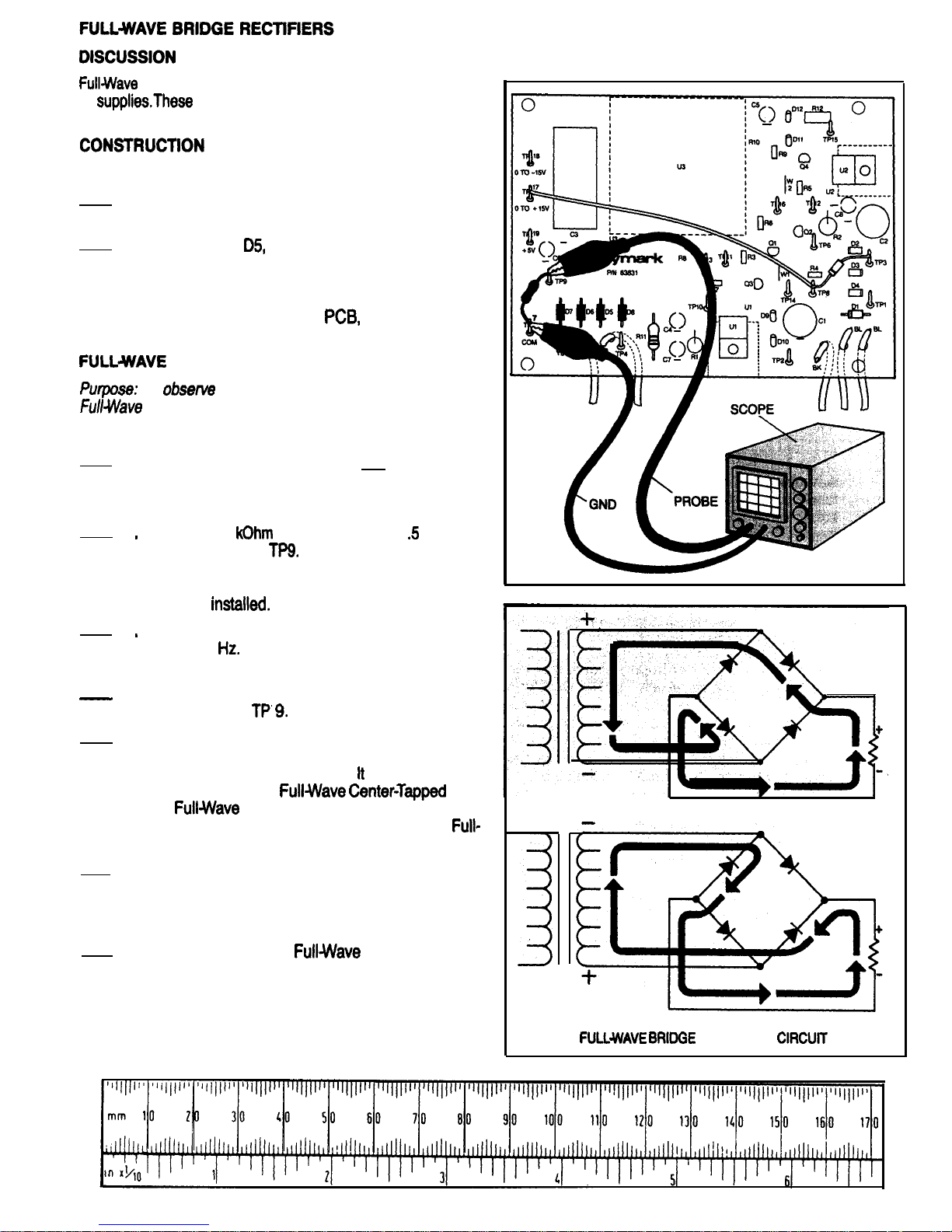
Refer to Fig. 47 for the following steps.
1
.
2
,
Be sure the 808 power plug is Not connected to
a power outlet.
Mount diodes
D6, D7 and D8 on the PCB Be
sure the banded ends of the diodes are oriented
the same as the diode outlines that are silk
screened on the PCB. Using a heat sink, solder
each diode lead to the
and cut off any
excess lead length.
BRIDGE RECTIFIER EXPERIENCE
To
the voltage waveform produced by a
Bridge Rectifier circuit.
Equipment: Oscilloscope
1. Be sure the 808 power plug is Not connected to
a power outlet.
Refer to Fig. 47 for steps 3 through 6.
2
3
4.
5
.
6
.
7
.
Solder a 1.5
(brown-green-red)
Watt re-
sistor toTP7 and
Cut the leads off close to
the test points. This resistor is for testing purposes and will be left in place until the 5 Volt reg-
ulator is
Adjust the scope to display a 30 Volt (peak to
peak) 60
signal. Set the vertical (Y) input
coupling to DC.
Connect the scope ground lead to TP7 and the
input probe to
Plug the 808 Power Supply plug into an outlet.
Turn the Power Switch ON. Observe the waveform displayed on the scope.
should look like
Fig. 45. Both the
and
the
Bridge produce the same wave-
form. Figure 48 illustrates current flow in a
Wave Bridge Rectifier circuit.
Turn the 808 Power switch Off and disconnect
the power plug from the outlet. Disconnect the
scope ground lead and input probe from the test
points.
This completes the
Bridge Rectifier
Test. Have your instructor initial your progress
guide.
FIG. 47
RECTIFIER
FIG. 48
26
Page 27
CENTER-TAPPED
BRIDGE RECTIFIERS
DISCUSSION
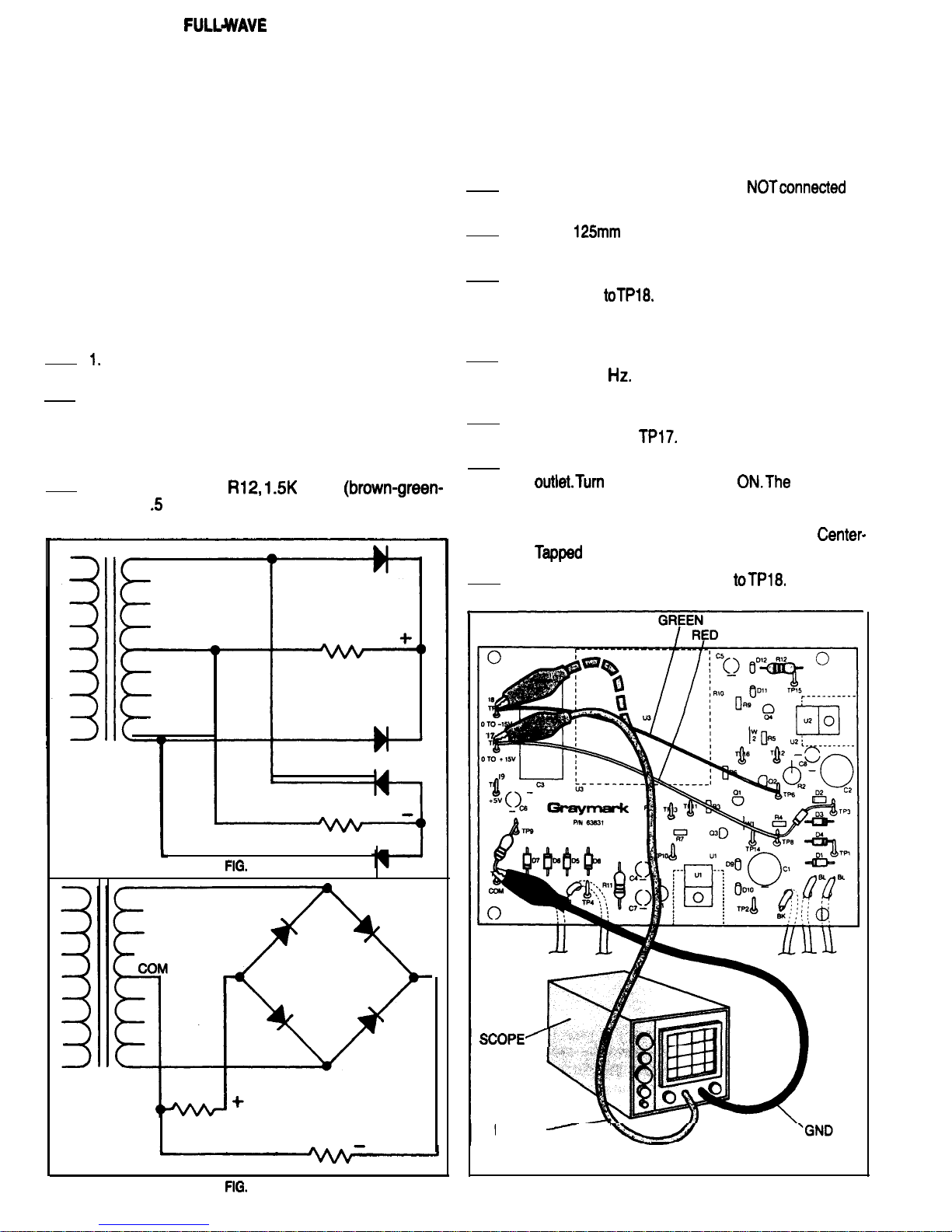
As mentioned before, the center-tapped full-wave bridge
rectifier circuit combines features of both the center-tapped
full-wave and the full-wave bridge rectifier circuits. It has
two equal voltage outputs of opposing polarity as referred
to the transformer secondary center tap. Figures 49A and
49B are schematics of the same rectifier circuit. Figure 49A
is drawn to illustrate that a center-tapped full-wave bridge
rectifier is made by connecting two center-tapped full-wave
rectifiers to a common center tapped transformer secondary winding. Figure 49B shows the same circuit, drawn differently to illustrate that a center-tapped full-wave bridge
rectifier can also be considered to be a full-wave bridge rectifier with a added center-tap on the transformer winding.
CONSTRUCTION
Refer to Fig. 50 tor the following steps.
Be sure the 808 power plug is not connected to
a power outlet.
2.
Mount diodes D3 and D4 to the PCB. Be sure the
banded ends of the diodes are oriented the
same as the diode outlines that are silk screened
on the PCB. Using a heat sink, solder each diode
lead to the PCB, and cut off any excess lead
3. Mount resistor Rl2,
Ohm
red),
Watt, on the PCB. Solder the resistor
leads to the PCB and cut off any excess length.
49A
CENTER-TAPPED FULL-WAVE BRIDGE RECTIFIER
EXPERIENCE
Purpose: To observe the voltages and waveforms pro-
duced by a Full-Wave Center-Tapped Bridge Rectifier
Circuit
Equipment: Oscilloscope
Refer to Fig. 50 for the following steps.
1.
Be sure the 808 power plug is
to
a power outlet.
2.
Cut a
length of green 22 gauge wire, and
strip 6mm of insulation from each end.
3.
Solder one end of the green wire toTP6, and the
other end
Because these are temporary
connections for testing purposes, it is not necessary to make mechanical connections.
4. Adjust the scope to display a 60 Volt (peak to
peak) 60 Hz signal. Set the vertical (Y) input
coupling to DC.
5. Connect the scope ground lead to TP7 and the
input probe to
6. Connect the 808 Power Supply plug to a power
the Power Switch
waveform
displayed on the scope should look like Fig. 45.
This is the same waveform being produced by
the same circuitry as in the Full-Wave
Rectifier Test that you did earlier.
7. Move the scope input probe
The wave-
form displayed on the scope now should look like
PROBE
49B
FIG. 50
27
Page 28
FULL WAVE RECTIFICATION, NEGATIVE OUTPUT
51
NO
CENTER-TAPPED
BRIDGE RECTIFIER
52
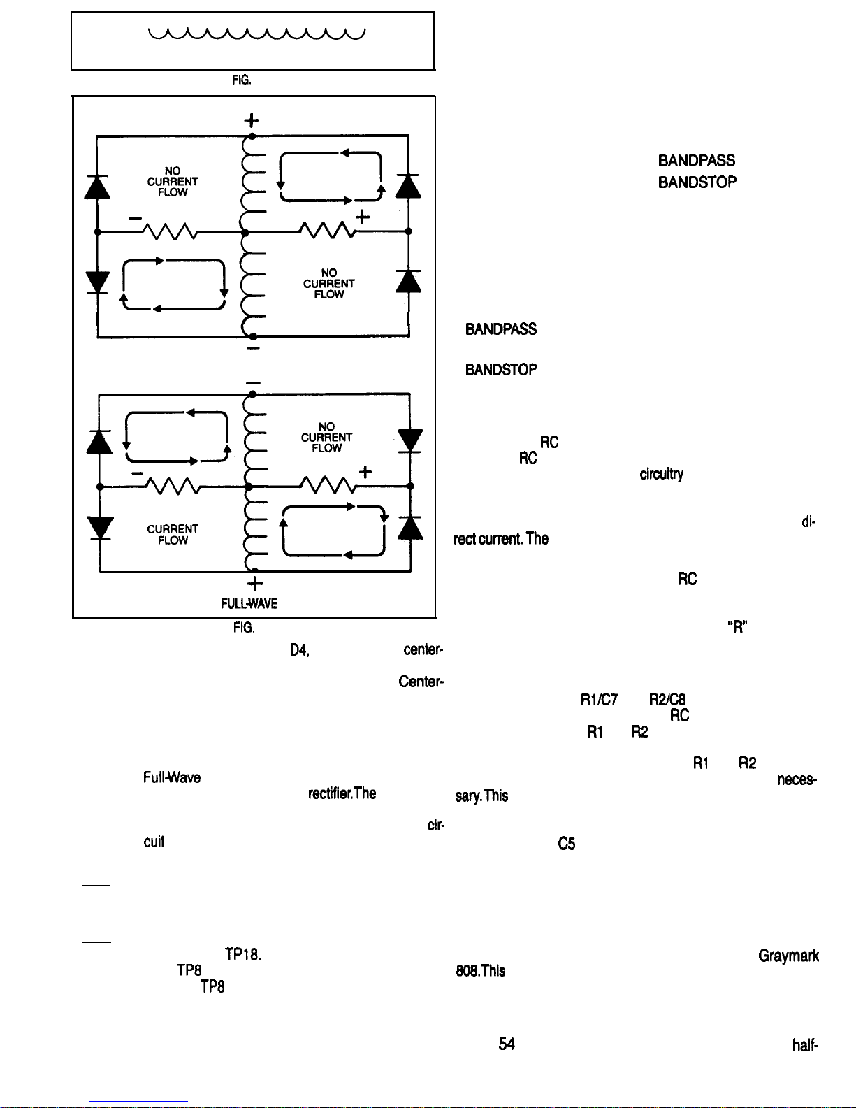
Fig. 51. Diodes D3 and
along with the
tapped secondary winding that also is connected
to diodes Dl and D2, form a Full-Wave
Tapped Rectifier the output of which is negative
in respect to the transformer center-tap. These
two complimentary Full-Wave Center-Tapped
Rectifiers, sharing the same transformer winding, can also be correctly called a Center-Tapped
Bridge Rectifier. Figure 52 shows the
current flow in this type of
transformer primary winding and core symbol have been
omitted so that the current flow in the rest of
can be shown clearly, but apart from that, it
is the same as Figs. 49A and 49B.
8. Turn the power switch Off and disconnect the
power plug from the outlet. Disconnect the scope
leads.
9. Unsolder and remove the green wire running
from TP6 to
Leave the red wire running
from
to TP17 and the diode connected to
TP3 and
in place, as you will be using them
later in another test.
-10
This completes the CENTER-TAPPED FULL
WAVE BRIDGE RECTIFIER EXPERIENCE.
Have your instructor initial your Progress Guide.
FILTER SECTION
DISCUSSION
In general, a filter is an electronic device used to pass a certain frequency or band of frequencies while rejecting or
blocking another frequency or band of frequencies.
There are four types of filters commonly used in
electronics:
LOW PASS
HIGH PASS
A LOW PASS filter will pass all frequencies from DC to a
cutoff frequency. All frequencies above this cutoff are attenuated. DC has a frequency of zero Hz; it is a straight line
on an oscilloscope.
A HIGH PASS filter will pass all frequencies above a cutoff
frequency, and attenuate all frequencies below that cutoff
frequency.
A
filter will pass a band or group of frequen-
cies, and attenuate all frequencies outside that band.
A
filter will attenuate a particular band of fre-
quencies and will pass all other frequencies.
To remove the ripple from the output of the rectifier circuit,
most power supplies use a resistance/capacitance filter
(also called a
filter) of the low pass type.The resistance
part of the
filters in most DC power supplies is provided
by the resistance of the diode
and the power trans-
former secondary winding, along with the reactance of the
power transformer. The term reactance applies to devices
operating on alternating current and varying (pulsating)
output of a rectifier circuit is an example
of pulsating direct current.
The resistance and reactance in a
filter used in a DC
power supply serves to limit the peak current flowing
through the rectifier diodes to a value that the particular
diodes being used can handle safely. The
part of the
filter does not directly enter into the filter’s effectiveness.
Figure 53 shows part of the block diagram and schematic
of the 808 Power Supply, with the capacitive filters high-
lighted. Notice that
and
are not highlighted.
These components appear to be
low pass filters, but
are not. the resistors
and
are current sensing resistors used in the overcurrent detectors of the variable positive and negative power supplies. If
and
were not
in the circuit, capacitors C7 and C8 would not be
is due to the characteristics of the integrated circuit voltage regulators Ul and U2, And will be discussed
in the External Control and Protection Circuitry Section.
Capacitors C4,
and C6 are also required because of
other characteristics of the voltage regulators. This will be
explained later in the section on voltage regulators.
CAPACITIVE FILTERS
DISCUSSION
NO half-wave rectifier circuits are used in the
experience included tests using a half-wave recti-
fier because, when done along with tests using a full wave
rectifier, they will help you to understand the operation of
capacitive filters.
Figure
shows the circuit you built earlier for the
wave rectifier test. The voltage waveform across resistor
28
Page 29
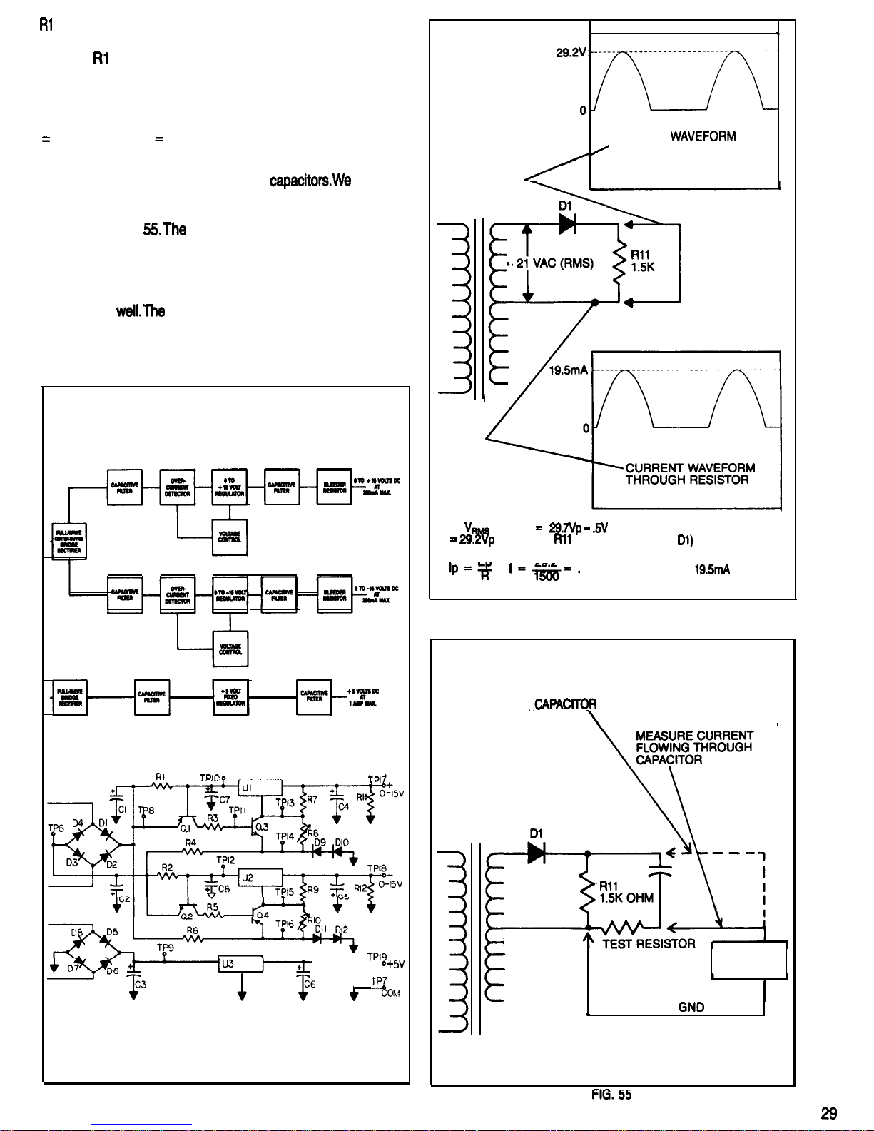
1 is what you saw in step 7 (Fig. 42). If we could connect
the scope so that it would display the current flowing
through
1, we would see that current waveform is the
same as the voltage waveform. We can say that the current
flowing through a resistor is in phase with the voltage
across the resistor, and is proportional to this voltage.
Ohms Law expresses this proportionality in the formula I
E/R or, current
voltage/resistance.
This direct correspondence of current and voltage are not
true with other components such as
can display the waveform and magnitude of the current passing
through a capacitor by using the test set up shown schematically in Fig.
voltage developed across the test
resistor is proportional to the current flowing through it. As
long as the resistance value of the test resistor is small
compared to the resistances in the circuit being tested, the
measurement error because of the added resistance will
be small as
high sensitivity of the oscilloscope allows the current sensing test resistor to have a small resistance value.
,
FIG. 53
VOLTAGE
ACROSS RESISTOR
Tl
21
x 1.414
(FORWARD VOLTAGE DROP
ACROSS
.
ACROSS
EP
29.2
0195 AMPERES OR
FIG. 54
PROBE CONNECTION TO MEASURE VOLTAGE
ACROSS
PROBE CONNECTION TO
Tl
10 OHMS
SCOPE
l
--
Page 30
CAPACITIVE FILTER EXPERIENCE
Purpose: To obsetve the current through and the voltage
across a capacitor when it is connected to a half wave
circuit.
Equipment: Oscilloscope
Clip Lead
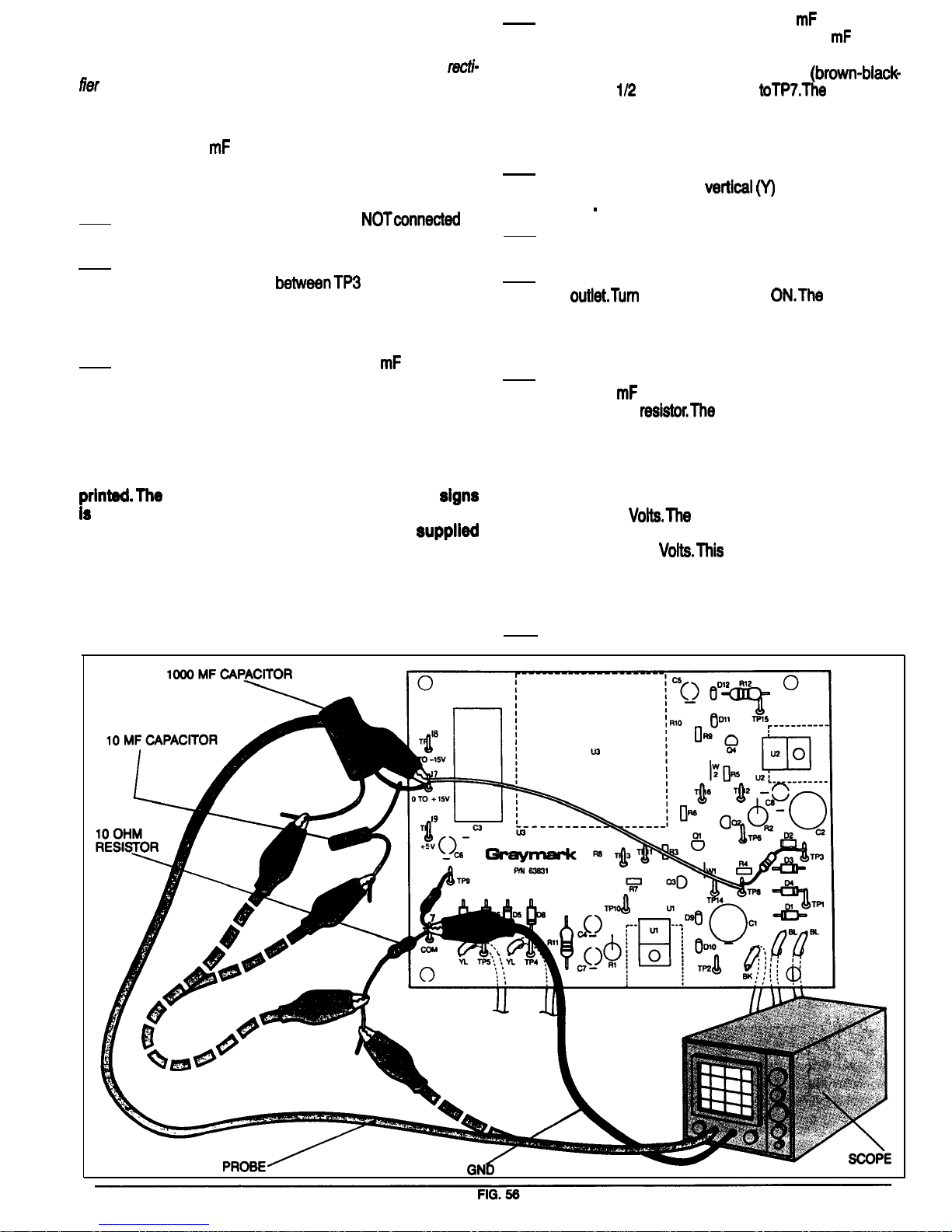
1000
Capacitor
Test Resistor
Refer to Fig. 56 for the following steps.
1.
Be sure the 808 power plug is
to
a power outlet.
2. Unsolder from TP3 the anode lead of the diode
that was installed
and TP8 during
the Full-Wave Center-Tapped Rectifier Test.
Bend the anode lead so that is not touchingTP3
or any of the other parts or the PCB.
3.
Solder the positive lead of a 1000
35 Volt ca-
pacitor toTP17. Make sure that the red wire from
TP8 remains soldered to TP17.
NOTE: The capacitors supplied in your 808 kit ail are
of the electrolytic type, and have both leads coming
out of one end of the body of the capacitor. On the side
of the capacitor there will be one or more minus signs
lead that is closest to these minus
the negative lead of the capacitor; the other lead is
the positive lead. Also, the capacitors are
with the positive leads longer than the negative leads
as a further means of determining polarity.
It is important to observe polarity when using electrolytic capacitors. Failure to do so may result in damage
to the capacitor and other components.
4. Solder the positive lead of a 10
50 Volt ca-
pacitor to the positive lead of the 1000
capac-
itor that you soldered to TP17 in step 3. Solder
one of the leads of the 10 Ohm
black)
Watt test resistor
other lead
of this 10 Ohm resistor and the negative leads of
the two capacitors are not connected to anything
at this time.
5. Adjust the scope to display a 30 Volt (peak) 60
Hz signal. Set the
input coupling to
DC
6. Connect the scope ground lead toTP7, and the
scope input probe to TP17.
7. Connect the 808 Power Supply plug to a power
the Power Switch
scope display should look like Fig. 57. You’ve seen this
waveform before, its the output of a half wave
rectifier.
8. Using a clip lead, connect the negative lead of
the 10
test capacitor to the free lead of the 10
Ohm test
scope should now display
the waveform shown in Flg. 58. Adjust the sweep
and trigger controls as necessary to make the
scope display closely match the waveform as
shown in Fig. 58. Notice that the peak voltage is
about 30 Volts, and the minimum voltage is
about 9
peak to peak ripple voltage is
the difference between these two voltages, that
is, about 21
is a very large amount of
ripple. If your stereo system were powered by a
supply with this much ripple, you would hear a
very loud 60 Hz tone whenever it was turned on.
9. Remove the 808 power plug from the outlet for
30
Page 31
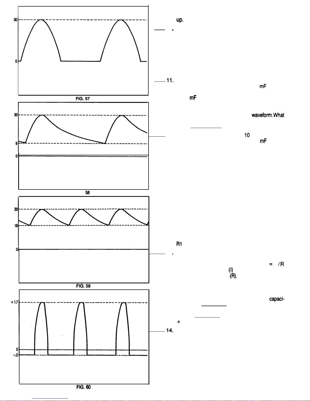
FIG.
10
12.
13
this step. Resolder the anode lead of the temporary D2 diode toTP3. Do not change the test set
Plug the 808 power plug back into the outlet. The
waveform on the scope should now look Fig. 59.
The peak voltage is still about 30 Volts, but the
minimum voltage has gone up to 18 Volts, and
the peak to peak ripple has gone down to 12
Volts. This shows that the output of a full wave
rectifier is more easily filtered than the output of
a half wave rectifier.
Disconnect the end of the clip lead that is connected to the negative lead of the 10
test ca-
pacitor, and connect it to the negative lead of the
1000
test capacitor. Observe the scope dis-
play. (You may need to readjust the scope trigger
control.) Using a colored pencil, draw this waveform on Fig. 59, over the printed
is the approximate peak to peak ripple voltage
now?
Move the Scope probe to the
Ohm test resis-
tor lead that is connected to the 1000
capacitor negative lead by the clip lead. You will need
to change the scope vertical Volts/cm control to
a more sensitive setting, as the voltage developed across the 10 Ohm resistor by the current
flowing through the test capacitor is quite low.
The waveform displayed on your scope should
look like the one shown in Fig. 60. Notice that
the current flows through the capacitor in short
positive pulses. These current pulses occur
when the instantaneous voltage from the rectifier
diodes exceed the the relatively constant voltage
across the capacitor. It is during these pulses that
the capacitor is charged or, to say it in another
way, that electrical energy is stored in the capacitor. During the longer periods between the posi-
tive current pulses the capacitor discharges, or
gives up electrical energy to the load resistor
1 and the 10 Ohm current sensing resistor.
We can use Ohm’s law to calculate the current
flowing through the capacitor during the charging
and discharging periods. The formula I
E
will give us the current
if the voltage (E) is di-
vided by the resistance
Using -0.2 Volts, the
voltage developed across across the current
sensing test resistor during capacitor discharge
periods, and 10 Ohms, the resistance value of
the current sensing resistor, calculate the
torcurrent.
Amps. Calculate the peak
capacitor current during the capacitor charging
period.
Amps. Hint: the voltage is
1.7 Volts.
Disconnect the 808 power plug from the power
outlet and the scope probe and ground lead from
your test setup. Unsolder the two capacitors, the
test resistor, the diode and the red wire that were
soldered to test points on the PCB. This completes the Capacitive Filter Experience. Have
your instructor initial your progress guide.
31
Page 32
CAPACITIVE FILTER CALCULATIONS
PERCENT OF RIPPLE
This term is often used to express how “clean” or free from
periodic voltage variations a power supply output is. The
voltage output of a battery supplying power to a constant
load, such a fixed resistor, has a percent of ripple of 0.
To calculate the percent of ripple, the following formula is
used:
V
Ripple
x 100
average
Where:
the rms value of the peak to peak
ripple voltage
We can use
times the peak to peak ripple voltage to determine the rms ripple voltage. While this
conversion is only exact for sine waveforms, it is
reasonably accurate for full-wave ripple
waveforms.
V
average
the average dc voltage output of the
power supply.
The dc voltage ranges of a VOM or a DMM read
the average value of a pulsating dc voltage input.
Using the above formula, calculate the percentage of ripple
in the voltage waveform shown in Fig. 59. Use 24.4 Volts
for V
Hint: the peak to peak ripple voltage can be calculated from
the voltage values given in Fig.
positive peak of the
ripple voltage is 30 Volts. The negative peak of the ripple
voltage is
Volts. Both of these voltages are positive in
respect to ground. The peak to peak ripple voltage is the
difference between these two voltages, that is, 12 Volts.
Write your answer here.
CAPACITANCE REQUIRED FOR A PARTICULAR
APPLICATION
we were designing a power supply, ho.w would we deter-
mine the value of capacitance needed for the capacitance
filter? Lets go through the process step by step, using the
positive 0 to
Volt power supply of the 808 as an example.
Figure 61 is the schematic of this power supply.
Determine the current required from the capacitive filter.
The rated output is
Volts at 300
Bleeder resistor
1 has a resistance value of 1500 Ohms. Using Ohm’s
law, E/R), we find the current through this resistor
is .OIO Amps, or 10
To calculate the current flowing through the
and
circuit, we will have to get some values from
the ELECTRICAL CHARACTERISTICS OF THE
table in
SECTION
of this manual. These values are the “Reference Voltage”, which appears across
and the “Adjustment
Pin
Reference Voltage is 1.30 Volts maxi-
mum.
is a 340 Ohm resistor. Using Ohm’s law again,
the same formula as above, the current through
cal-
culates to be 3.8
Since the Adjustment Pin Current
is a relatively low 100
(or .l
we will ignore it. If
we wanted to include it, it would be added to the current
flowing through
Since a current of 300
is not
enough to turn on the
protection
and
there is no current flowing
a
30
0
.
Dropout Voltage
-25
0
25 50 75
100 125 150
TEMPERATURE
through these three components. Its as if they were not
there.
Adding these three currents gives us the total current
that the filter capacitor (Cl
must provide during the time
periods that the rectifier is not supplying current. See
Fig. 60.
Rated output current:
300.0
Bleeder
1) current:
10.0
Voltage control circuit current:
3.8
Total current: 313.8
2.
Determine the voltage required from the capacitive filter.
The rated output is 15 Volts. To this we must add the
“Drop Out” voltage of the voltage regulator, and the voltage drop across the overcurrent sensing resistor Rl.
The drop out voltage of a regulator is the lowest voltage
across its input to output terminals that can exist with the
voltage regulator still functioning as a regulator. We will
get voltage from the Dropout Voltage graph, from the
National Semiconductor specification sheets for the LM
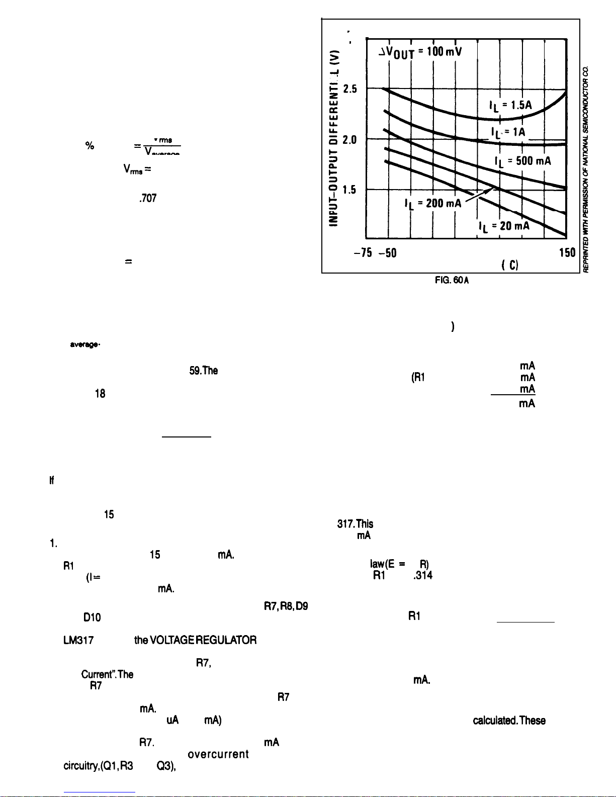
graph is shown in Fig. 60A. Using a current of
500
and a temperature of 25 C, the graph indicates
the input/output differential to be about 1.8 Volts.
Ohm’s
I x
indicates the voltage drop across
1 Ohm
to be
Volts.
Rated output voltage: 15.0
Volts Regulator dropout voltage:
1.8
Volts
voltage drop:
0.314 Volts
Total Voltage: 17.114 Volts
This is the minimum voltage that Cl has to maintain between the time periods the rectifier is supplying current
if the output voltage is to be maintained at 15 Volts with
a current of 300
3.
If complete specifications for the power transformer and
rectifier diodes are available, the peak voltage at the
bridge rectifier output can be
specifications would have to include winding resistances, turn
ratios,. and core losses at different power levels for the
power transformer and forward voltage drops at different current levels for the rectifier diodes.
32
Page 33
PEAK VOLTAGE OF 22.2 VOLTS
62
63
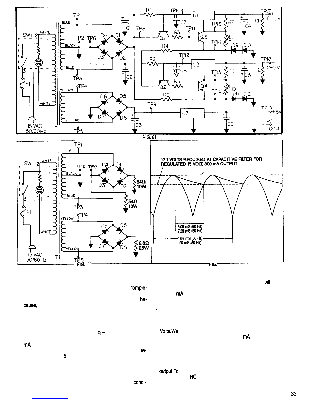
A less math-intensive, more empirical method would be
tions the measured peak output voltage of the rectifier
to provide resistive loads for each rectifier output, and
is 22.2 Volts. We need to maintain a voltage of at least
measure the peak D.C. voltage available to charge the
17.1 Volts (which is 77% of the peak voltage) at
times
filter capacitor with an oscilloscope. (The word
to maintain a regulated power supply output of 15 Volts
cal” relates to information gained by observation and
at 300
How big a capacitor will be needed to do
experimentation.) All the outputs need to be loaded
this?
due to the primary winding resistance and core
losses of the transformer, increasing the load on one
winding will decrease the voltage output of the other
windings. Figure 62 shows schematically how this
measurement would be made.The load resistor values
are calculated with the formula: E/l. For the variable supplies, we use the values of 17.1 Volts and 314
that we calculated earlier. The two load resistors
have a resistance value of 54 Ohms each.The load
sistor for the fixed
Volt supply was calculated in a simi-
lar manner, and has a resistance value of 6.8 Ohms.
The input voltage to the power transformer is reduced
to 95 Volts, as this is the minimum input voltage specified for the 808 Power Supply. Under these test
4
Through calculation and measurement, we have determined that the power transformer and rectifier are capable of providing a full wave pulsating DC voltage of 22.2
Volts at full rated current with a line input voltage of 95
have also determined that to maintain a regu-
lated plus 15 Volts at a current of 300
at the variable
positive output of the 808 Power Supply, the voltage
from rectifier will have to be at least 17.1 Volts at all
times. Figure 63 shows this information graphically,
along with the period of time that the capacitive filter will
have to supply power during each cycle of the rectifier
calculate the size of the capacitor needed, we
will be using
time constant formulas.
n
Page 34
TIME CONSTANT EXPERIENCE
DISCUSSION
The time constant of the discharge of a capacitor through
a resistor is the time required for the voltage or current to
drop to 1
of its value at the time the discharge began.The
symbol “e” is the base of the natural or Napierian logarithm.
value is 2.718. The reciprocal of e (l/e) is 0.3679.
Consider the formulas:
EC
x
or;
EC
x
Where:
is the voltage across the capacitor at
the end of the discharge time period,
is the voltage across the capacitor at
the beginning of the discharge period,
e is 2.718,
is the discharge time in seconds,
T
x C, in seconds,
is resistance in Ohms,
and C is capacitance in Farads.
If
is expressed in
C in
in milliseconds
the formula is a little easier to handle.
Using a 1000
capacitor and a 10
resistor,T (that
is,
is 10,000
or 10 seconds. If
is 10 Volts, and
is 10 seconds,
then
10 x 0.3679’
3.679 Volts.
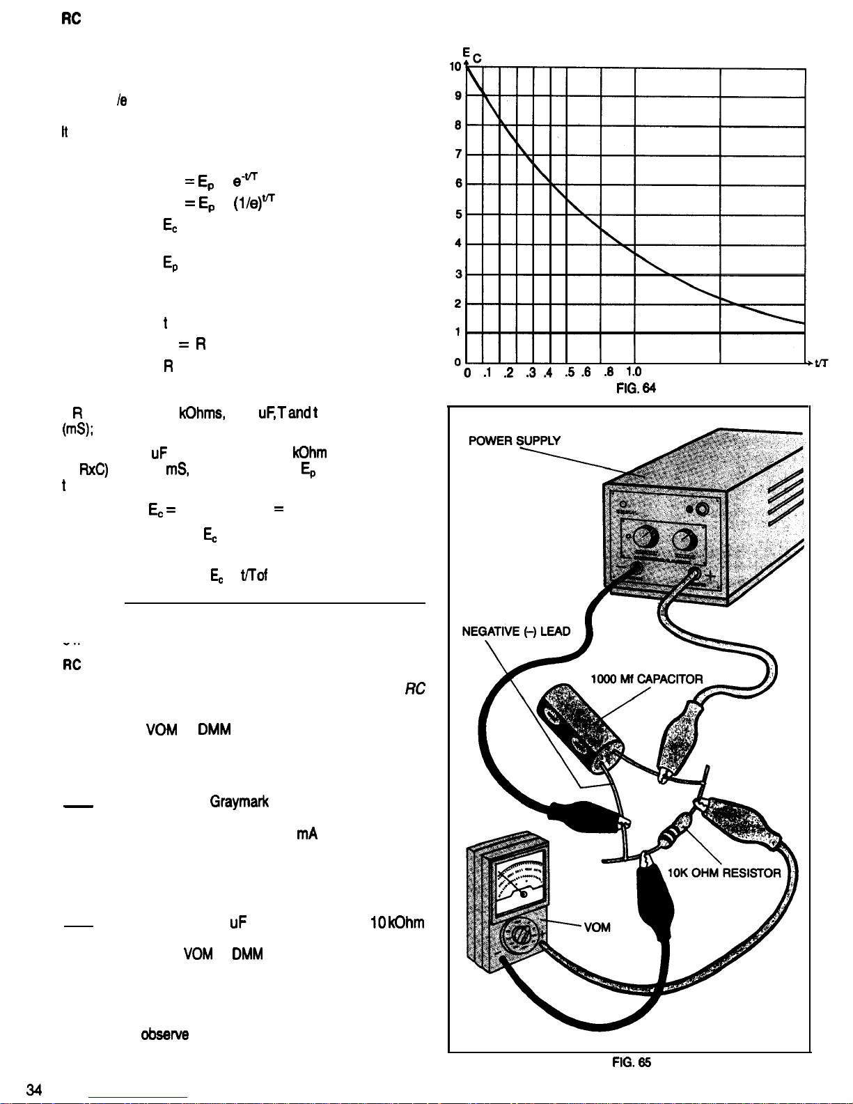
Figure 64 is a graph of
versus time, using the values giv-
en above.
Calculate the values for
at
0.5 and 2.0. Record your
answers.
Compare your answers with the values you read from Fig.
64
CIRCUIT TEST
Purpose: To observe the action of an actual (hardware)
circuit.
Equipment:
or
1.
2
.
DC Power Supply
Two Clip Leads
Watch With Second Hand or Digital Readout
A completed
808 or 803 Power Supply, or any power supply capable of supplying 10
Volts at approximately 25
or more may be
used. Be sure the power supply power plug is
Not connected to a outlet, and that the voltage
control is set for minimum voltage output. Refer
to Fig. 65 for the following steps.
Connect a 1000
capacitor and the
(brown-black-orange) test resistor from your 808
kit to the
or
as shown in Fig. 65. Solder the capacitor leads to the resistor leads. Do
not make a mechanical connection of the leads
before soldering, as these parts will be
unsoldered at the end of this experience. Be sure
to
the capacitor polarity when connect-
ing the power supply and meter.
1B
1.5
2.0
Page 35
X
10
9
CAPACITANCE REQUIRED FOR A
(continued)
With some understanding of
time constants, we can
continue with the capacitive filter calculations that were be-
gun
power transformer and rectifier circuitry for
the positive variable power supply of the 808 are capable
of supplying a full wave pulsating DC voltage of 22.2 peak
Volts at full rated current with a line input voltage of 95
Volts.
For the voltage regulator and overcurrent protection circuit-
ry to maintain an output of
Volts at a current of 300
the voltage from the rectifier will have to be at least 17.1
Volts at all times.The length of time that the capacitive filter
will have to periodically supply power to maintain this minimum voltage is 7.29
for
Hz input power. Refer to
Fig. 63 to review this information. The equivalent load resistance of the fully loaded voltage regulator and
overcurrent circuitry is 54 Ohms.
The formula:
(I
can be rewritten to solve for
1
0
0123456 8 10
15
20
3
4
l
6
8
FIG.66
Set the test meter to read a voltage of 10 Volts
DC. Connect the power supply plug to an outlet
and adjust the power supply for a meter reading
of 10 Volts.
Disconnect one of the clip leads from the power
supply, wait 20 seconds and then read the meter.
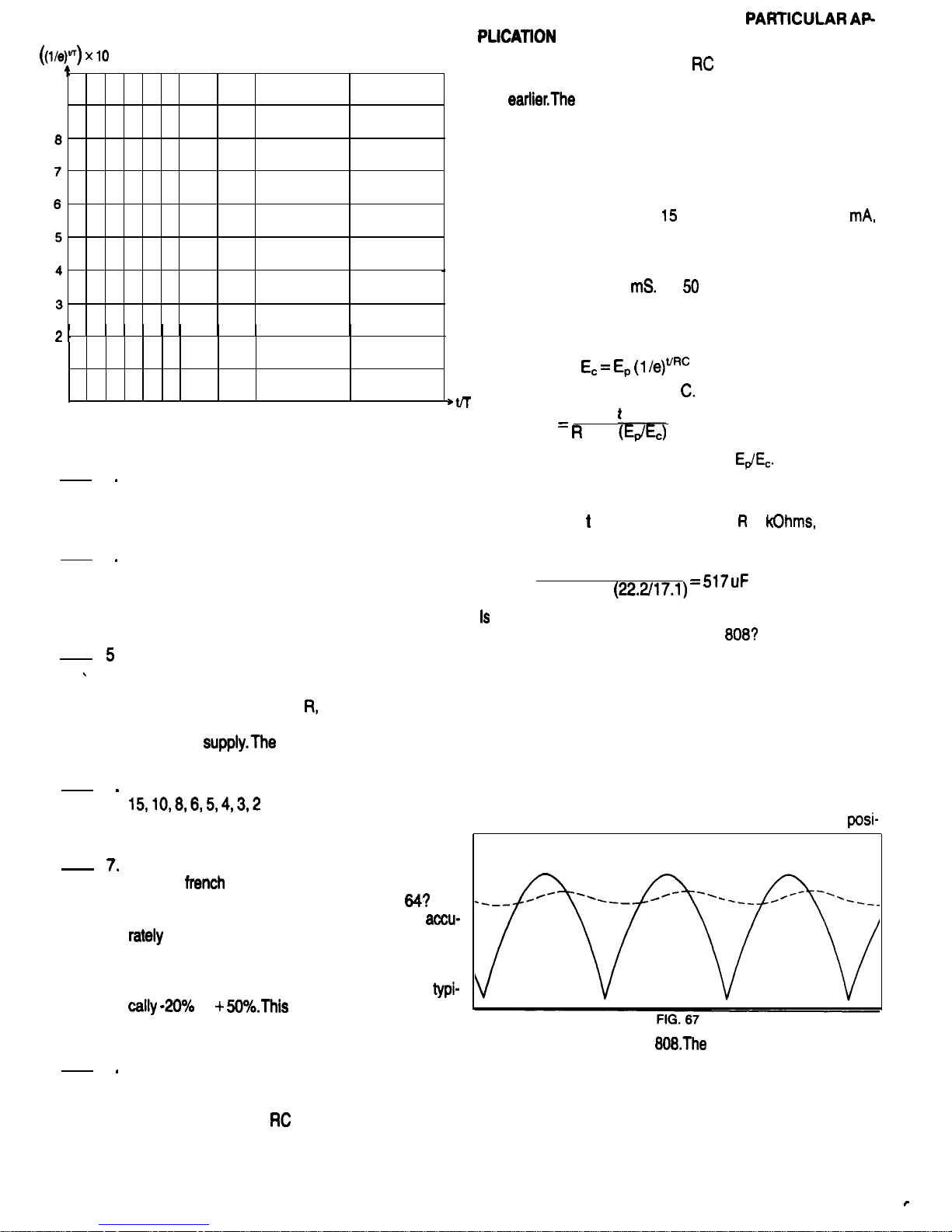
Put a dot on the blank graph in Fig. 66 where the
voltage you read from the meter and the time you
waited intersect.
Reconnect the clip lead (that was disconnected
in step 4) to the power supply. Notice how rapidly
the capacitor is charged to 10 Volts. This is because the resistance, or
is now only the clip
lead resistances plus the internal resistance of
the power
total of these resistances
is probably less than 100 Ohms.
Repeat steps 4 and 5, using waiting periods of
and 1 seconds. Place a dot
in the appropriate place on the graph in Fig. 66
each time you repeat steps 4 and 5.
Connect the dots on the graph with a pencil line,
using a
curve if possible. Does the graph
you just drew look like the one in Fig.
Be-
cause of the difficulty in reading the meter
when the voltage is changing rapidly, the
dots you place near the left edge of the graph will
be the least accurate. Also, the capacitance tolerances of electrolytic capacitors are large,
to
could affect the vertical
location of the curve you generated on the graph,
but not necessarily its slope.
Remove the power supply plug from the outlet.
Disconnect the clip leads and the meter test
leads Unsolder the capacitor and resistor leads.
This completes the
Time Constant Experi-
ence- Have your instructor initial your progress
guide.
C
x In
In is the natural log of, in this case,
It can be found
by using a table of natural logarithms or a scientific
calculator.
By expressing
in milliseconds and
in
C will be
in microfarads. Plugging in these values and solving for C,
we get:
7.29
0.054 x In
this the value that should be used for the capacitive filter
for the positive variable supply in the
Because of one
factor that we were not able to evaluate in our empirical design approach, the answer to that question has to be “no”.
Look at Fig. 60 again. This figure shows the voltage drop
across a current sensing resistor connected between the
rectifier and the capacitive filter. Because of the winding resistance and core losses of the power transformer, and
losses in the rectifier circuitry, the spikes of current that oc-
cur when the capacitive filter is charging will reduce the
voltage available at the rectifier output.
Figure 67 shows the full wave rectifier output for the
tive variable supply of the
solid line shows the voltage waveform with a resistive load and no capacitive filter.
The dashed line shows the voltage waveform when a capacitive filter is added. Notice how the voltage peaks are
reduced with the addition of the filter.
To determine the values for the capacitive filters empirical-
ly, trial values for the capacitors must be connected and the
i
Page 36
power supply outputs evaluated under load until
capacitance values are found. Most engineering compa-
nies use a mathematical approach for the initial design
work, and then verify the design by building and testing a
prototype. Developments in computers and software allow
tests using computer simulated prototypes, with savings in
engineering time and expense.
A value of 1000
was selected for the capacitive filter of
the positive variable supply in the
808. The se-
lection of this value was based on further calculations.
CONSTRUCTION
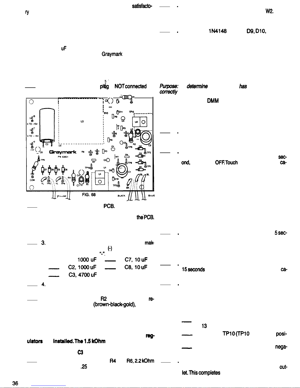
Refer to Fig. 68 for the following steps.
1.
Be sure the 808 power
is
to
a power outlet.
0
,
2. Mount diode D2 on the
Be sure that the
banded end of the diode is oriented the same as
the diode outline that is silkscreened on
Using a heat sink as shown in Fig. 40, solder the
diode leads to the PCB. Cut off any excess lead
length.
Mount the following capacitors on the PCB,
ing sure that the negative
leads are inserted
into the holes marked
-A. Cl,
D.
B.
E.
C.
Solder all the capacitor leads to the PCB and cut
off any excess lead lengths.
5. Mount resistors RI and
on the PCB. Both
sistors are 1 Ohm
1 Watt.
Solder the resistor leads to the PCB and cut off
any excess lead length.
NOTE: The following components are being mounted
on the PCB at this time to serve as bleeder resistors
for capacitors Cl and C2 until the variable voltage
are
test resistor which
was connected to TP7 and TP9 earlier serves as a
bleeder for capacitor
until regulator U3 is installed.
6.
Mount and solder resistors
and
(red-red-red),
Watt, on the PCB. Cut off the
excess lead length. Save one of these leads for
the next step.
7
8
Bend the piece of wire saved from the last step
into a “U” shape, and use it for Jumper
insert
this jumper wire from the component side of the
PCB. Solder and cut off any excess lead length.
Mount the
diodes
Dll and
D12 on the PCB. These diodes are smaller than
the rectifier diodes installed earlier. Be sure that
the banded ends of the diodes are oriented as
shown on the diode outlines printed on the PCB.
Using a heat sink, as shown in Fig. 40, solder the
diodes to the PCB. Cut off any excess lead
PCB TEST
To
that the PCB
been assembled
up to this point.
Equipment: VOM or
1
2
3
4
5
6
Watch with second hand or digital readout.
(Counting out loud “One thousand one, one
thousand two . . .
one thousand thirteen” etc.,
would be accurate enough for these tests.)
Review rule 9 of BUILDING YOUR POWER
SUPPLY BREADBOARD that appears earlier in
this manual.
With the 808 power plug connected to a power
outlet, turn the 808 power switch ON, wait 1
and turn it
all the diodes and
pacitors C7 and C8 with your finger to tell if any
of them are warm or hot. Bigger components
take longer to heat up if something is wrong. By
checking smaller components after a short power ON period, even if something is wrong the
components probably will not be damaged, and
will work satisfactorily after the fault is wrrected.
If any of the wmponents called out above are
warm, something is wrong. Check the PCB carefully, and consult with your instructor if
necessary.
Repeat step 2, leaving the power ON for
onds. Recheck all the diodes, and capacitors C7
and C8 to tell if they are warm. In addition, touch
capacitors Cl, C2 and C3 to tell if they are getting
warm.
Repeat step 2 again, leaving the power ON for
this time. Recheck all diodes and
pacitors for heating.
If none of the diodes or capacitors heated up in
steps two through four, power up the 808 again
and measure the dc voltage between the pairs of
test points listed below. For an input line voltage
of from 105 to 125 Volts, the voltages you measure should be within the ranges listed below.
A. TP7 and TPQ (TPQ should be positive),
to 16 Volts dc.
B. TP7 and
should be
tive), 25 to 31 Volts dc.
C. TP7 and TP12 (TP12 should be
tive), 25 to 31 Volts dc.
Turn OFF the power switch of the 808 Power
Supply, and remove its power plug from the
the FILTER SECTION. Have
your instructor initial your progress guide.
Page 37
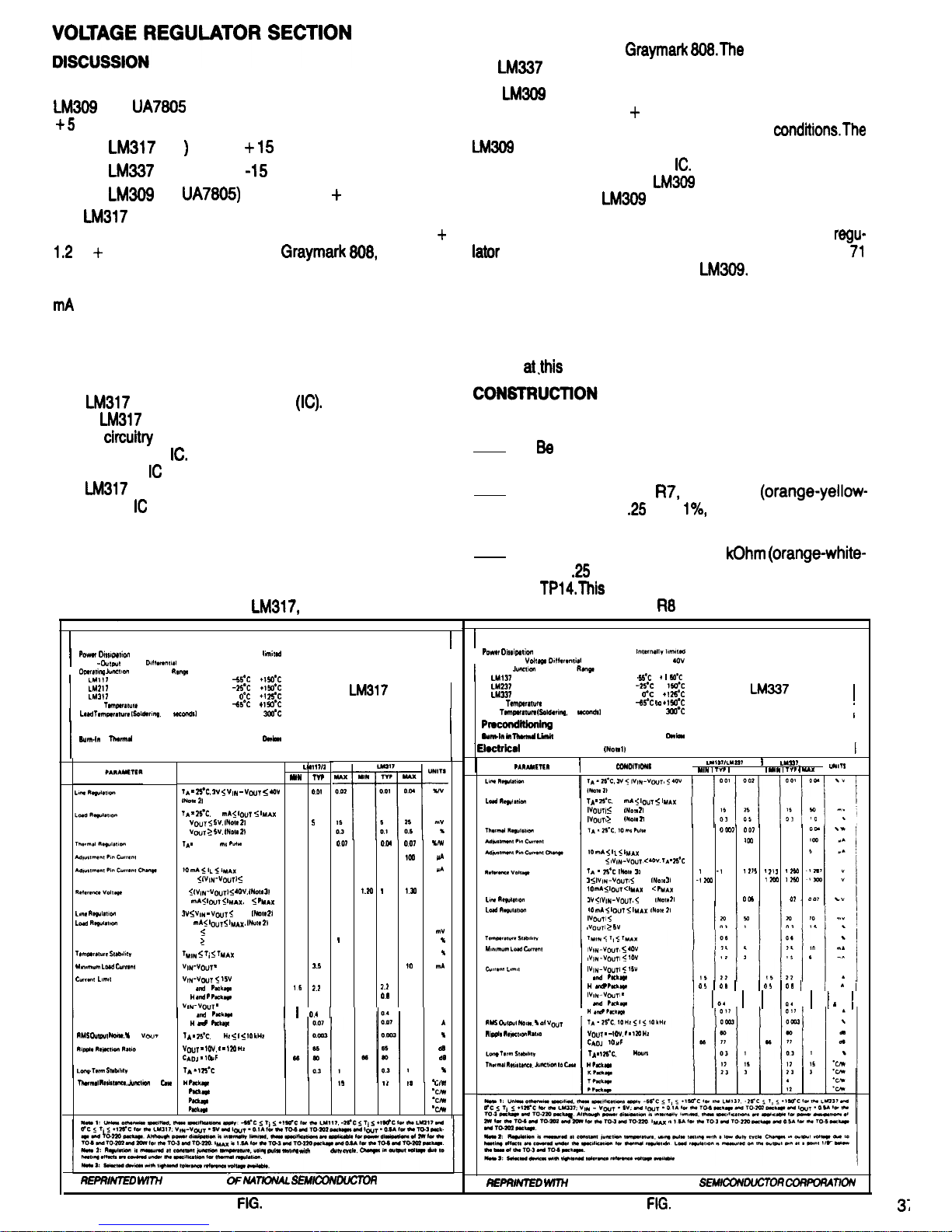
is adjustable from -1.2 to -37 Volts. It is used in the negative
variable supply of the
specifications for
the
are shown in Fig. 70.
The 808 uses three voltage regulators as follows. The
and
are interchangeable devices for the
VDC supply.
(Ul
for the VDC supply
(U2) for the
VDC supply
(or
(U3) for the
5 VDC supply
The
is a nonadjustable three terminal device, and
is used to regulate the
5 VDC supply so the output volt-
age is constant under varying load and line
is an integrated circuit, and all of the circuitry to do
it’s job is contained within the
Current limiting is also in-
cluded in the design of the
to limit the output current
to safe value. The
also has internal thermal shut-
down protection circuitry to prevent it from overheating. If
the internal power dissipation becomes too great, the
will shutdown to prevent damage to itself. Figure
shows the specifications for the
The
is a three terminal adjustable positive voltage
regulator. Refer to Fig. 69. Its output is adjustable from
to
37 Volts. As used in the
its output
is guaranteed to be adjustable upward to a minimum of a
regulated 15 Volts under worst case conditions, that is, 300
output current and low input line voltage (95 Volts AC).
The output voltage is adjustable down to 0 Volts. This is
made possible by the design of the external control circuitry. This will be discussed in the EXTERNAL CONTROL
AND PROTECTION CIRCUITRY section.
The three voltage regulators will be installed and tested one
at a time. Some of the associated circuit components have
already been installed so that tests could be performed,
and some of the voltage control components will be in-
stalled
time so that the regulators can be tested.
The
is an integrated circuit
All of the circuitry
for the
to do it’s job, with the exception of the voltage
divider
that controls the the output voltage, is con-
tained within the
Current limiting is also included in the
design of the
to limit the output current to a safe value.
The
also has internal thermal shutdown circuitry to
prevent the
from overheating. When the regulator reaches its maximum safe operating temperature, the regulator
will shutdown to prevent damage to itself by excessive
heating. All protection circuitry remains fully functional
even if the adjustment terminal becomes disconnected.
Refer to Fig. 72 for the following steps.
1.
sure the 808 power plug is not connected to
a power outlet.
2. Mount resistor
340 Ohm
black-black)
Watt
on the PCB. Solder the
leads to the PCB and cut off any excess length.
3. Solder the leads of a 3.9
red)
Watt test resistor to test pointsTP13 and
resistor temporarily takes the place of
The LM337 is similar to the
except that its output
variable resistor
for test purposes.
1
Absolute Maximum Ratings
Absolute Maximum Ratings
Input-Output
internally
Input
Voltage
4ov
Operating
Temperature
Temperature
to
to l
Storm
SPECIFICATIONS
Load
10
to
to
Storage
to
SPECIFICATIONS
10
100% All
Preconditioning
in
Limit
100% Ail
Electrical Characteristics (Note 1)
Characteristics
I
MAX
CONDITIONS
0.1
003
50
0.2
1.20 1.25
0.02
m
0.3
1
0.5 0.8
10
5V
5V
- 5
10
21
25°C. 20 ms
65
65
I 5
1
225
250
-1250
1300
007
0
100 50
S
0.2 5 IJA
130
2s
V
0.05 0.02 0.07 WV
50 20 70
03 15
1
5 3.5
15
A
05
A
2 5V
<
TA
40V.
P
40V
2 5V
40V
3
31
10
P
40V.
21
10
VOUT
5V
VOUT
5V
40V
K
T
hdLJ$,J
40V
K
T
5 5V
K
T
* 40V
K J”d T PJchJtfJ
I
of
*
10 Hz
HZ
A
to
12
K
23 3 2.3 3
T
4
P
12
01
RJUO
-
l
1000
.fuf!ctton
CJsJ
J tow
PERMISSION
CORPORATION
PERMISSION Of NATIONAL SEhflCOM?UCTOff
69
70
Page 38
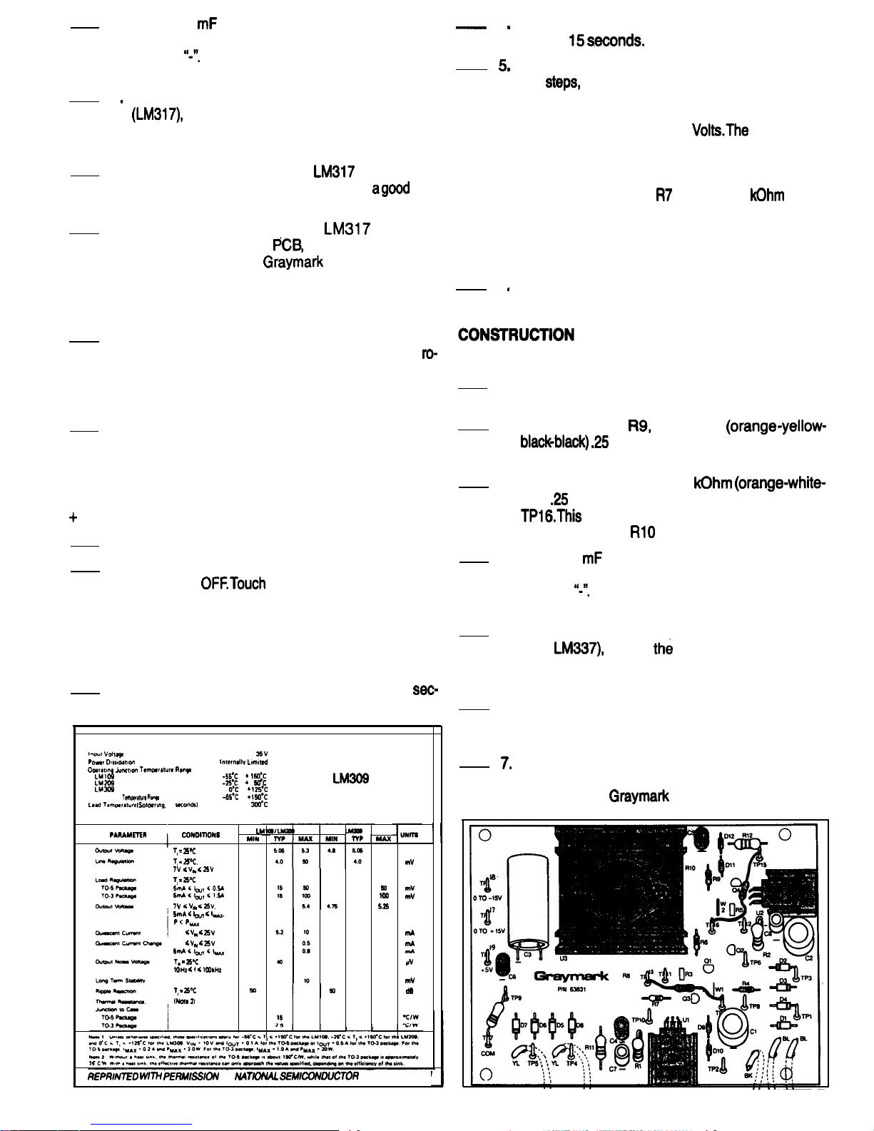
Repeat step 2 again, this time leaving the power
ON for
If none of the components heated up in the previ-
ous
power up the 808 again. Measure the
dc voltage between test points TP7 and TP17.
TP17 should be positive, and the voltage should
be between 12.7 and 15.8
reason that
a range of voltages is given is that the tolerances
of a number of components can affect the regula-
tor output voltage. If the voltage is not in this
range, check resistor
and the 3.9
resistor installed temporarily between TP13 and
TP14. Make sure they are the correct resistors
for these locations. Consult with your instructor
if necessary.
Turn OFF the 808 power switch and remove the
power plug from the power outlet.
Mount 10
capacitor C4 on the PCB, making
4
sure that the negative lead is inserted in the hole
marked
Solder the capacitor leads to the PCB
and cut off any excess length.
Locate the positive variable voltage regulator, U 1
one of the small heat sinks, a 3 x 8mm
machine screw, a 3mm split lock washer and a
3mm hex nut.
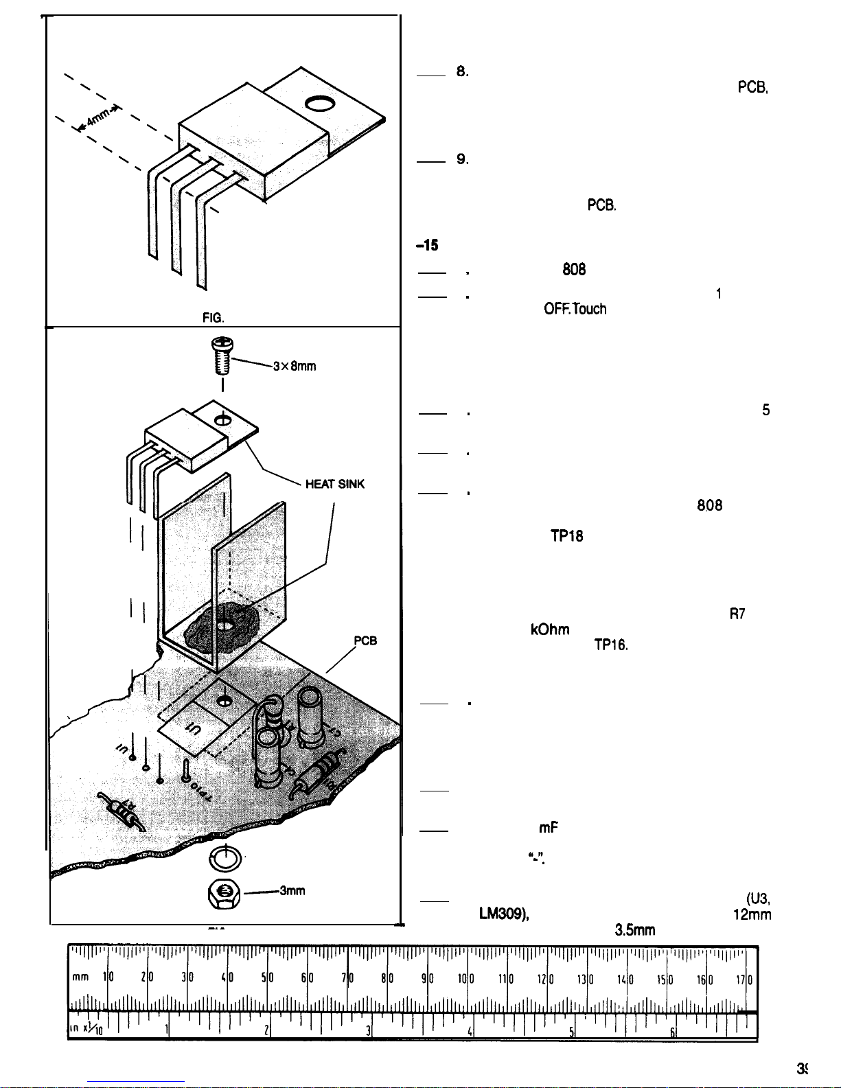
Bend the three leads of the
regulator as
shown in Fig. 73. A long nose pliers is
tool
to use for this.
Refer to Fig. 74. Mount the
regulator
and heat sink on the
using the hardware
called out in step 5.
recommends the
use of heat sink compound on the surfaces of
the voltage regulators and heat sinks where
they contact each other.
6
4
.
5
6
.
.
7
.
8
.
9
.
Before tightening the machine screw and nut that
holds the heat sink and regulator to the PCB,
tate the heat sink on the machine screw so that
its cooling fins are oriented as shown in Fig. 72.
Then tighten the machine screw and nut.
Solder the regulator leads to the PCB, using a
small alligator clip heat sink on each lead between the plastic regulator package and the top
surface of the PCB. Cut off any excess lead
length.
Refer to Fig. 72 for the following steps.
1. Be sure the 808 power plug is not connected to
a power outlet.
2. Mount resistor
340 Ohm
Watt 1%, on the PCB. Solder the
leads to the PCB and cut off any excess length.
3. Solder the leads of a 3.9
red)
Watt test resistor to test pointsTP15 and
resistor temporarily takes the place of
variable resistor
for test purposes.
15 VOLT REGULATOR TEST
1. Connect the 808 power plug to a power outlet.
2. Turn the 808 power switch ON, wait 1 second
and turn it
the components that were
installed in the construction steps that were just
completed. If any of these components are
warm, there is something wrong. Check the PCB
and components carefully, and consult with your
instructor if necessary.
4. Mount 10
capacitor C5 on the PCB, making
sure that the negative lead is inserted in the hole
marked
Solder the capacitor leads to the PCB
and cut off any excess length.
5. Locate the negative variable voltage regulator
(U2,
one of
small heat sinks, a 3 x
8mm machine screw, a 3mm split lock washer
and a 3mm hex nut.
3. Repeat step 2, leaving the power ON for 5
onds this time.
6. Bend the three leads of the LM337 regulator as
shown in Fig. 73. A long nose pliers is a good tool
to use for this.
Refer to Fig 74. Mount the LM337 regulator and
heat sink on the PCB, using the hardware called
out in step 5.
recommends the use of
Absolute Maximum Ratings
to
to
1
to
SPECIFICATIONS
Storage
to +150°C
10
Electrical Characteristics
T
T
15
15
5.2
40
15
2.5
47
4.6
V
V
<
7v
25v
7v
25v
25.T
5.2
50
10
0.5
0.0
20
OF
CORPORATION
FIG. 71
FIG. 72
38
Page 39
73
SCREW
COMPOUND
3mm SPLIT
/LOCK WASHER
NUT
FIG. 74
heat sink compound on the surfaces of the
voltage regulators and heat sinks where they
contact each other.
Before tightening the machine screw and nut that
holds the heat sink and regulator to the
rotate the heat sink on the machine screw so that
its cooling fins are oriented as shown in Fig. 72.
Then tighten the machine screw and nut.
Solder the regulator leads to the PCB, using a
small alligator clip heat sink on each lead
between the plastic regulator package and the
top surface of the
Cut off any excess lead
length.
VOLT REGULATOR TEST
1
2
3
4
5
6
Connect the
power plug to a power outlet.
Turn the 808 power switch ON, wait
second
and turn it
the components that were
installed in the construction steps that were just
completed. If any of these components are
warm, there is something wrong. Check the PCB
and components carefully, and consult with your
instructor if necessary.
Repeat step 2, leaving the power ON for
seconds this time.
Repeat step 2 again, this time leaving the power
ON for 15 seconds.
If none of the components heated up in the
previous steps, power up the
again.
Measure the dc voltage between test pointsTP7
and TP18.
should be negative, and the
voltage should be between 12.7 and 15.8 Volts.
The reason that a range of voltages is given is
that the tolerances of a number of components
can affect the regulator output voltage. If the
voltage is not in this range, check resistor
and
the 3.9
resistor installed temporarily
betweenTP15 and TPl6. Make sure they are the
correct resistors for these locations. Consult with
your instructor if necessary.
Turn OFF the 808 power switch and remove the
power plug from the power outlet.
CONSTRUCTION
Refer to Fig. 72 for the following steps.
1. Be sure the 808 power plug is not connected to
a power outlet.
2. Mount 10
capacitor C6 on the PCB, making
sure that the negative lead is inserted in the hole
marked
Solder the capacitor leads to the PCB
and cut off any excess length.
3. Locate the positive fixed voltage regulator
the large heat sink, two 3.5 x
machine screws, two
split lock washers
Page 40
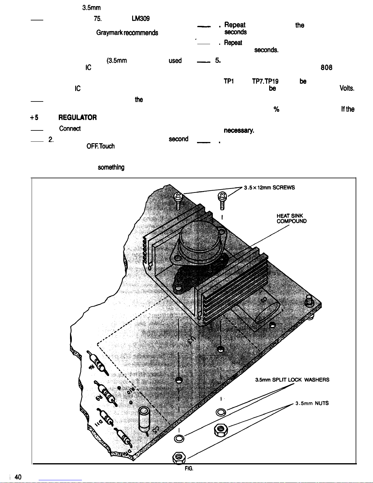
and two
nuts.
4.
Refer to Fig.
Mount the
regulator and
heat sink on the PCB, using the hardware called
3
out in step 3.
the use of
heat sink compound on the surfaces of the
voltage regulators and heat sinks where they
4
contact each other. Be sure that the larger
machine screws
diameter) are
to
fasten the
and heat sink to the PCB. If you use
the smaller 3mm diameter screws for this
purpose, it is possible for the heat sink to short
to the
leads.
5.
Solder the regulator leads to
PCB. Cut off any
excess lead length.
VOLT
TEST
1.
th8 808 power plug to a power outlet.
Turn th8 808 power switch ON, wait 1
6
and turn it
the components that were
installed in the construction steps that were just
completed. If any of these components are
warm, there is
wrong. Check the PCB
and components carefully, and consult with your
instructor if necessary.
step 2, leaving
power ON for 5
this time.
step 2 again, this time leaving the power
ON for 15
If none of the components heated up in the
previous steps, power up the
again.
Measure the dc voltage between* test points
9 and
should
positive, and the
voltage should
between 4.6 and 5.4
This range of voltages allows for the specified
output voltage tolerance (4.7 to 5.3 Volts), plus
approximately 2
measurement error.
voltage is not in this range, check your work
carefully, and consult with your instructor if
Turn OFF the 808 power switch and remove the
power plug from the power outlet.
75
Page 41
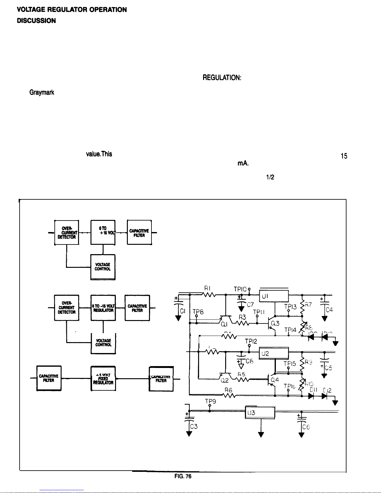
Figure 76 is a partial block diagram and schematic of the
808 Power Supply, showing the voltage regulators and
associated circuitry.
A power supply requires regulation to maintain a constant
voltage level with variations in load, AC line voltage, and
environmental conditions. Voltage regulators provide the
regulation which will enable the supply to maintain a
constant output voltage under these changing conditions.
The
808 is voltage regulated triple power supply.
The following are the definitions of load, and line regulation:
LOAD REGULATION: Load regulation is a supply’s ability
to maintain a constant voltage or current output level with
changes in a resistive load.
increases.This is because of the internal resistance of the
power supply. When the load resistance decreases, the
load current increases, causing a proportional increase in
the voltage drop across the internal resistance of the power
supply. This results in a decrease in the voltage at the
power supply output. Refer to Fig. 78.
LINE
Line regulation is a supply’s ability to
maintain a constant voltage or current output level with
changes in the input AC line voltage.
Figure 77 shows four voltage graphs plotted with a
common X axis, representing the passage of time.The top
graph is of AC line voltage. It appears that some other large
loads on this line are being switched on and off, resulting
in variations of the AC line voltage.
If the value of FULL LOAD voltage is equal to the value
of NO LOAD voltage, the LOAD VOLTAGE REGULATION
Two power supplies are connected to this power line. One
is 0%, which is the ideal
value means the power
is unregulated, the other is a regulated power supply. Both
supply is a true voltage source, where the output voltage
of these power supplies have nominal output ratings of
is independent of the current drawn from the supply.
Volts DC at 300
Both power supplies are driving
identical loads. These loads periodically change between
In an UNREGULATED power supply the output voltage
no load (infinite resistance),
load (100 Ohms resistance)
decreases as the amount current drawn from the supply
REGULATOR
. ,
,
R2
Page 42
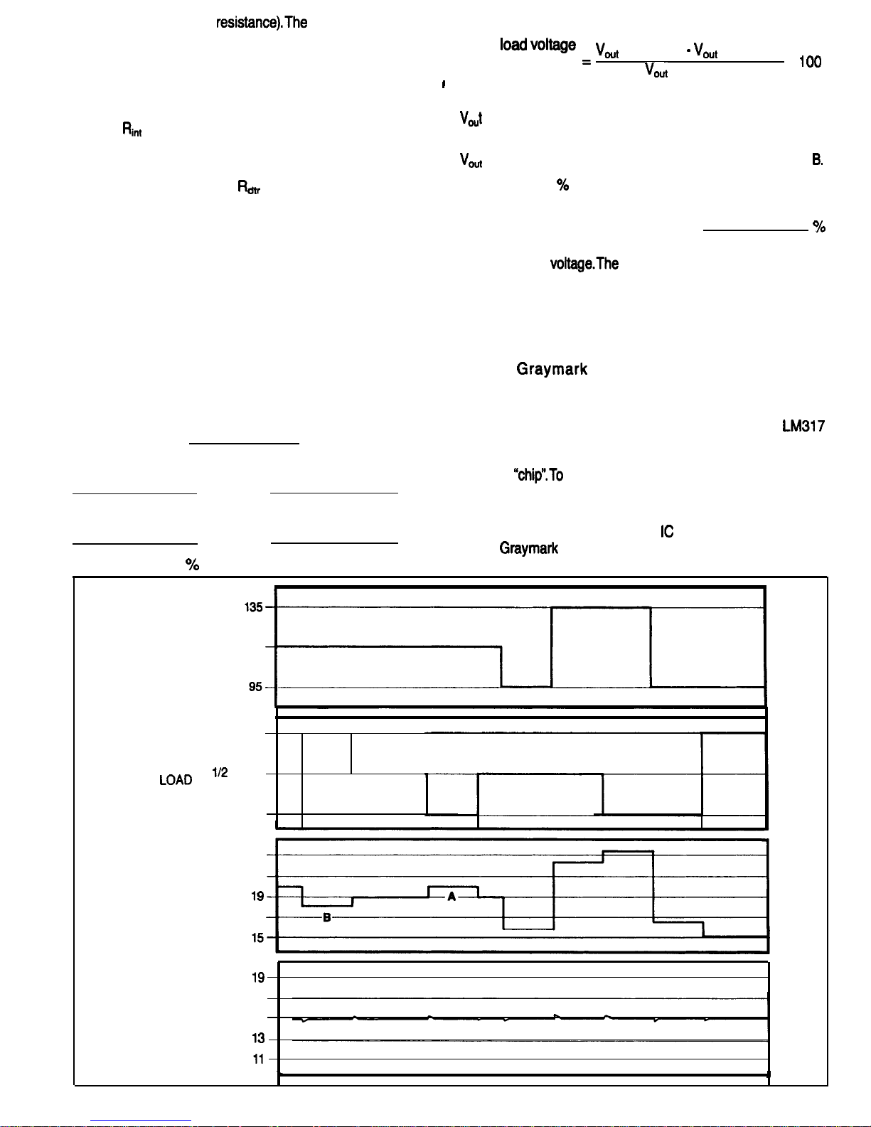
and full load (50 Ohms
changing condition
following formula:
of these loads is shown by the second graph.
%
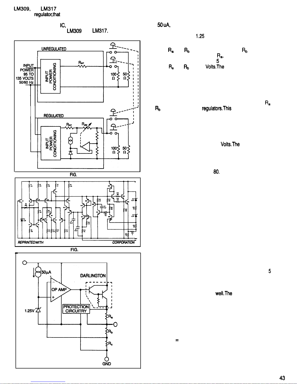
Figure 78 is the equivalent circuits of the unregulated and
regulation
(no load) (full load) x
the regulated power supplies. The boxes labeled INPUT
(full load)
POWER CONDITIONING represent the input circuitry,
At the nominal line input voltage of 115 Volts.
power transformer, rectifiers and input filters. The resistors
labeled
represent all the losses and resistances in the
(no load) occurs at the point on the Unregulated Power
components mentioned above.
Supply Output graph that is marked with the letter A.
(full load) occurs at the point marked with the letter
In the equivalent circuit of the regulated power supply, the
variable resistor labeled
represents the Darlington
transistor in the voltage regulator that controls the current
that flows through the regulator to the load resistors. The
load resistors are shown with push-button switches,
ganged together between the two loads. With this setup,
the load conditions shown in the second graph could be
duplicated by manipulating the switches.
Calculate the
load voltage regulation for this power
supply and write your answer in the space provided.
The bottom graph in Fig. 77, shows the regulated power
supply output
little “glitches’ appearing on this
graph indicate that the voltage regulator cannot instantly
compensate for input voltage and load changes. More
about that later.
How voltage regulators actually work will be discussed in
more detail a little later. Right now we just want to see the
differences in the output voltages of unregulated and
regulated power supplies with varying line input voltages
and loads.
The third graph from the top shows the output voltage of the
unregulated power supply. What is the worst case voltage
variation in Volts?
Most real life regulators won’t provide the zero percent
regulation shown on the graph, but the voltage regulators
in your
808 Power Supply will provide
considerably better than 1% combined line and load
regulation.
Figure 79 shows the schematic diagram of the
voltage regulator. Transistors, resistors, Zener diodes and
Under what conditions is the output voltage the highest?
capacitors are formed in a small piece of silicon, often
called a
help understand how a voltage regulator
Input line.
Load.
functions, we will be using a functional schematic, which
Under what conditions is the output voltage the lowest?
is shown in Fig. 80.
Input line.
Load.
The operation of all three of the
voltage regulators used
in the
808 Power Supply is based on the same
To calculate the
load voltage regulation, use the
general principles. The following discussion applies to the
INPUT
LINE 115
VOLTAGE
FULL LOAD
(50 OHMS)
LOAD
(100 OHMS)
NO LOAD
23
21
UNREGULATED
POWER SUPPLY
OUTPUT (VOLTS) 17
17
REGULATED
POWER SUPPLY 15
OUTPUT (VOLTS)
FIG. 77
42
Page 43
the
and the LM337. The LM337 is a
negative
is, its input and output voltages are
negative in respect to ground. This results in different
polarities inside the
but it operates according to the
same principles as the
and
POWER SUPPLY
POWER SUPPLY
78
PERMISSION OF NATIONAL SEMICONDUCTOR
79
INPUT
,
TRANSISTOR
OUTPUT
The two overlapping circles and the arrow in the upper left
hand corner of the schematic form the symbol for a current
source. A current source will pass a constant current, in this
case
despite variations of the voltage appearing
across its terminals. This current source provides a
constant current for the Volt Zener diode that supplies
the reference voltage for the regulator.
Resistors
and
form a voltage divider.
has three
times the resistance in Ohms of
so when the voltage
at the regulator output terminal is
Volts, the voltage at the
junction of
and
is 1.25
operational amplifier
(op amp) compares this portion of output voltage of the
regulator to the 1.25 Volt reference voltage. As long as the
two input terminals of the op amp are at the same voltage,
there is very little current flowing either into or out of the op
amp output terminal.
The adjustable voltage regulators are a little different.
and
are external to the
will be discussed
later in the EXTERNAL CONTROL AND PROTECTION
CIRCUITRY section.
If we increase the voltage regulator load by connecting a
resistor between the regulator output and ground, the
additional current flowing through the regulator will cause
the output voltage to drop below 5
voltage at the
op amp input terminal marked with the minus sign drops
as well. The op amp responds to this input change by
moving its output in a positive direction, causing an
increase in the base current of the Darlington transistor
shown at the right side of Fig.
The Darlington transistor is named after the person who
invented this particular way of connecting two transistors
and a resistor together to form the equivalent of one
transistor. A Darlington transistor requires very little base
input current to control the collector output current, and can
respond to rapid changes of the base current.
A transistor can be thought of as a valve that controls the
flow of electrons, that is, the current in a circuit. The “valve
handle” of the transistor is its base. The amount of current
flowing through the transistor from emitter to collector is
controlled by a much smaller current flowing from the
emitter to the base.
Another way of looking at a transistor is to consider it as a
variable resistor, where an increase in the base current
causes a decrease in the resistance.
At this point, the output of the voltage regulator is below
Volts because an additional load resistor was connected
between its output terminal and ground. This lowered
output voltage caused the voltage at the inverting input of
the op amp to become lower as
op amp responds
to this input voltage change by by moving its output in a
positive direction, increasing the base current of the
Darlington transistor.
The resulting decrease of resistance between the
Darlington transistor’s emitter and collector causes an
increase in the current flowing through the voltage
regulator and the load resistors. In accordance with Ohm’s
law, (voltage
current x resistance), the output voltage of
the voltage regulator heads back up to 5 Volts.
Figure 81 shows the effects of connecting a load resistor
to the output of a voltage regulator. The conditions shown
in the right portion of the figure occur after the load resistor
FIG. 80
Page 44
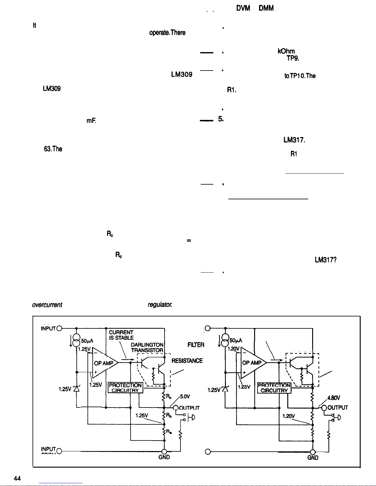
is connected, but before the voltage regulator. is able to
Equipment:
or
compensate for this change in load resistance.
takes much longer to describe the operation of a voltage
1
regulator than it takes for the regulator to
is
some time delay from the instant that a load change or
input voltage change takes place and causes the output
voltage to change until the voltage regulator is able to
2
compensate and restore the correct output voltage. This
time delay occurs mostly in the op amp and Darlington
3
transistor circuitry. Figure 82 is from the
specification sheets, and illustrates the time required for
the
regulator to respond to a load change. Notice
that it is a very short time, about 1 micro second.
The output filter capacitor for the fixed supply, C6, reduces
4
the amplitude of these voltage spikes. C6 has a
capacitance of 10
It does not need to have a large
capacitance like C3, the input filter capacitor, because of
the short periods of time it must provide or absorb electrical
energy to keep the output voltage constant. Look again at
Fig.
time that the input filter capacitor must provide
electrical energy is about 6 milliseconds, which is 6000
times as long as 1 microsecond.
The circuitry symbolized by the rectangle labeled
PROTECTION CIRCUITRY can divert the op amp output
current away from the base of the Darlington transistor.
Normally, when the op amp output moves in the positive
direction, we want to increase the current flowing through
the voltage regulator and load resistor. But when this
current reaches the maximum value the regulator can
safely handle, we don’t want it to increase any more.
The voltage across resistor
is directly proportional to the
current flowing through it. (Ohm’s law again, voltage
current x resistance. As the output current of the regulator
increases, the voltage across
increases as well. When
this voltage reaches a level that indicates the maximum
safe current is flowing, the protection circuitry begins to
divert current away from the Darlington transistor base.
OVERCURRENT PROTECTION EXPERIENCE
6
7
Clip Lead
Be sure that the 808 power plug is NOT
connected to a power outlet. Refer to Fig. 83 for
the following steps.
Remove the 1.5
test resistor which is
soldered toTP7 and
Connect the positive meter lead toTP8 and the
negative meter lead
meter will read
the voltage across the current sensing resistor
Set the meter range selector to read a DC
voltage of 2.5 Volts.
Connect the 808 power plug to a power outlet.
Turn the 808 power switch ON. While observing
the meter, connect the clip lead from TP7 to
TP17. This is a short circuit across the positive
variable regulator,
This represents a
heavy overload for the power transformer and
current sensing resistor
. Read the meter and
quickly remove the clip lead. Write down the
meter reading here.
Volts
Using Ohm’s law, calculate how much current is
flowing through the regulator.
Amps. Notice that
when using a 1 Ohm current sensing resistor,
The voltage across the resistor in Volts is the
same as the current flowing through the resistor
in Amps. The same correspondence occurs
when voltage is in millivolts, the current is then
in milliamps. How does the current you
measured compare to the value given on the
National Semiconductor Electrical Characteris-
tics specification sheet for the
Turn OFF the 808 power switch and remove the
power plug from the power outlet. Disconnect the
clip lead and the meter test leads.
Purpose: To observe the operation of the internal
Just how hot a voltage regulator becomes when it is
limiting function of a voltage
operating depends on a number of variables. The input
POSITIVE
FROM
FILTER
POSITIVE
INPUT
FROM
CURRENT
WILL INCREASE
.
DARLINGTON
TRANSISTOR
RESISTANCE
WILL
DECREASE
IS STABLE
LOAD
RESISTOR
NEGATIVE
FROM
FILTER
LOAD
RESISTOR
NEGATIVE INPUT
FROM FILTER
FIG. 81
Page 45
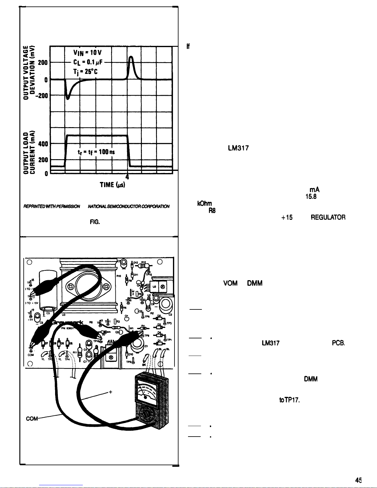
LOAD TRANSIENT RESPONSE
0
1
2
3
5
6
OF
82
FIG.
83
voltage, along with the output current and voltage, affect
the amount of power that the regulator has to dissipate.The
size of the heat sink and the amount air flow around it
affects how much the temperature of the regulator must
rise to dissipate this power.
a voltage regulator gets too hot, it will be damaged, even
though the current flowing through it is within safe limits.
The protection circuitry on the voltage regulator chip
includes a temperature sensor. When the chip temperature
reaches its maximum safe limit, the protection circuitry
begins to divert some of the op amp output current from the
Darlington transistor base, just as it did when the regulator
output current reached its maximum safe value, as we
discussed earlier.
OVER TEMPERATURE PROTECTION
DISCUSSION
To force the
voltage regulator into its over
temperature protection mode without risking damage to
other power supply components, the regulator will be
operated without a heat sink attached while supplying
approximately the maximum rated current of the power
supply. The 50 Ohm 5 Watt test resistor that will be used
for a load draws between 254 and 316
with the
regulator output voltage between 12.7 and
Volts. The
3.9
test resistor that was installed in place of variable
resistor
sets the regulator output within this range. If you
wish to, refer back to step 5 of the VOLT
TEST
TEMPERATURE PROTECTION EXPERIENCE
Purpose: To observe a voltage regulator and its output
when if is in the over temperature protection mode.
Equipment: Oscilloscope
or
50 Ohm 5 Watt Test Resistor
Drinking Straw
1. Be sure that the 808 power plug is NOT
connected to a power outlet.
Refer to Fig. 84 for the following steps.
2
3
.
4
5
6
Temporarily remove the mounting hardware and
heat sink for the
regulator from the
Solder the 50 Ohm test resistor leads toTP7 and
TPl7.
Connect the ground lead of the scope and the
negative lead of the DVM or the
to the test
resistor lead going to TP7. Connect the scope
probe and the positive lead of the meter to the
test resistor lead going toTPl7. Adjust the meter
and scope to read and display a 15 Volt DC
signal.
Connect the 808 power plug to a power outlet.
Turn the 808 power switch ON. Watch the meter
and scope display. Depending on the ambient
temperature and the power line voltage, it may
take a minute or more for the voltage regulator to
reach the temperature at which the over
Page 46
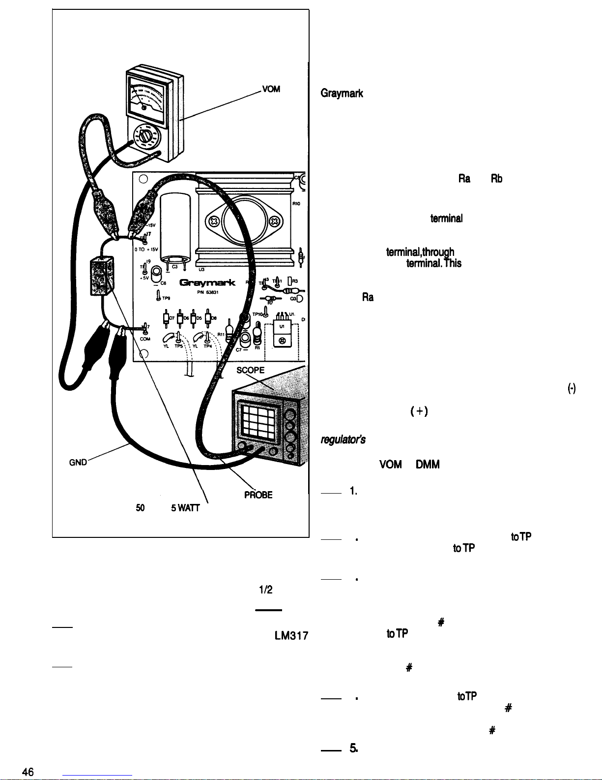
OHM
T&T
RESISTOR
FIG. 84
temperature protection circuitry begins to
operate. When the over temperature circuit is
activated, the voltage across the test resistor will
begin to drop. Wait approximately
minute
longer. What is the meter reading?
Volts
7.
While watching the meter and scope display, use
the drinking straw to blow on the
regulator. What happens?
8. Turn OFF the 808 power switch and remove the
power plug from the power outlet. Disconnect the
test equipment and unsolder the test resistor.
Replace the heat sink and mounting hardware
that was removed in step 2.
This completes the TEMPERATURE PROTECTION
EXPERIENCE. Have your instructor initial your progress
chart.
EXTERNAL CONTROL AND PROTECTION
CIRCUITRY SECTION
VOLTAGE CONTROL
DISCUSSION
Figure 85 is a partial block diagram and schematic of the
808 Power Supply, with the external voltage
control circuitry highlighted.
Figure 86 is a functional diagram of the positive adjustable
regulator and its external voltage control circuitry. The
negative adjustable regulator is similar, but with reversed
voltage polarities. Comparing this schematic with the
functional schematic of the fixed voltage regulator shown
in Fig. 80, we see that resistors
and
are now outside
the regulator, and that the ground terminal has become the
adjustment terminal.
Because the adjustment
Is the control Input of the
voltage regulator, the current necessary to operate the op
amp and protection circuitry inside the regulator must flow
from the input
the regulator circuitry and
through the output
is why there needs to be
some output current flowing whenever the regulator is
operating. The bleeder resistor and the voltage control
resistors,
and Rb, provide the load needed to cause this
current flow.
ADJUSTMENT VOLTAGE EXPERIENCE
The voltage that is applied to the adjustment terminal of a
voltage regulator determines the output voltage of that
regulator. The op amp inside the regulator adjusts the
resistance of the Darlington transistor so that the voltage
at the op amp’s inverting input (marked with a minus
sign) is the same as the voltage at its non-inverting input
(marked with a plus
sign).
Purpose: To demonstrate how an adjustable voltage
output responds to different voltages at the
adjustment terminal.
Equipment:
or
Clip Lead
Be sure the 808 power plug is not connected to
a power outlet.
Refer to Fig. 87 for the following steps.
2
3
4
Connect the negative meter lead
7 and the
positive meter lead
17. Set the meter to a
range that will read up to 20 Volts DC.
Connect the 808 power plug to an outlet and turn
the power switch ON. Write the voltmeter reading
down in Fig. 88 in the “Output Voltage” column
and the Clip Lead Connections “None” row (in
the box marked
1). Move the negative meter
lead
13 and write the voltmeter reading in
the “Output to Adjustment Voltage Difference”
column and the Clip Lead Connections “None”
row (box
2). Set the meter range selector to a
lower range if necessary for an accurate reading.
Connect the clip lead
13 and TP 2. Write the
meter reading down in box
3. Move the
negative meter lead back to TP 7 and write the
meter reading down in box
4.
Disconnect the negative meter lead from TP 7
Page 47
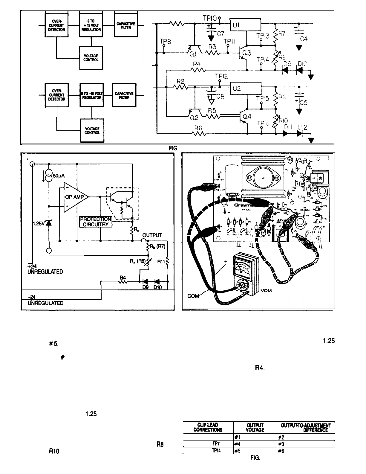
RI
85
INPUT
DARLINGTON
TRANSISTOR
ADJUSTMENT
COMMON
VOLTS
FIG. 86
FIG. 87
while you change one end of the clip lead from
TP 2 to TP 14. Reconnect the negative meter
lead to TP 7 and write the meter reading in box
Move the the negative meter lead from TP
7 to TP 13 and write down the meter reading in
box
6.
Notice that while the output voltage changed
when the adjustment terminal of the voltage
regulator was connected to different voltages,
the output-to-adjustment voltage difference
remained the same.The op amp was controlling
the Darlington transistor resistance so that the
op amp’s input terminals remained at the same
voltage- The
Volts across the output and
regulator output voltages.
When the adjustment terminal is connected to
ground, the regulator output voltage is
Volts. To be able to adjust the output voltage to
0 Volts, two diodes connected in series are
forward biased by the unregulated negative
supply, through
The exact voltage drop
across the diodes will vary with the current
flowing through them and their temperature, but
it is approximately 1.4 Volts, or 0.7 Volts for each
diode.This results in the variables supplies being
adjustable to and a little beyond zero Volts. With
the voltage controls turned all the way down, the
adjustment terminals of the regulator is actually
the voltage of the voltage reference inside the
regulator.
VOLTAGE
NONE
.
,
Later, when you connect potentiometers
and
TP13 TO
to the PCB, they will control the adjustable
TP13 TO
88
47
Page 48
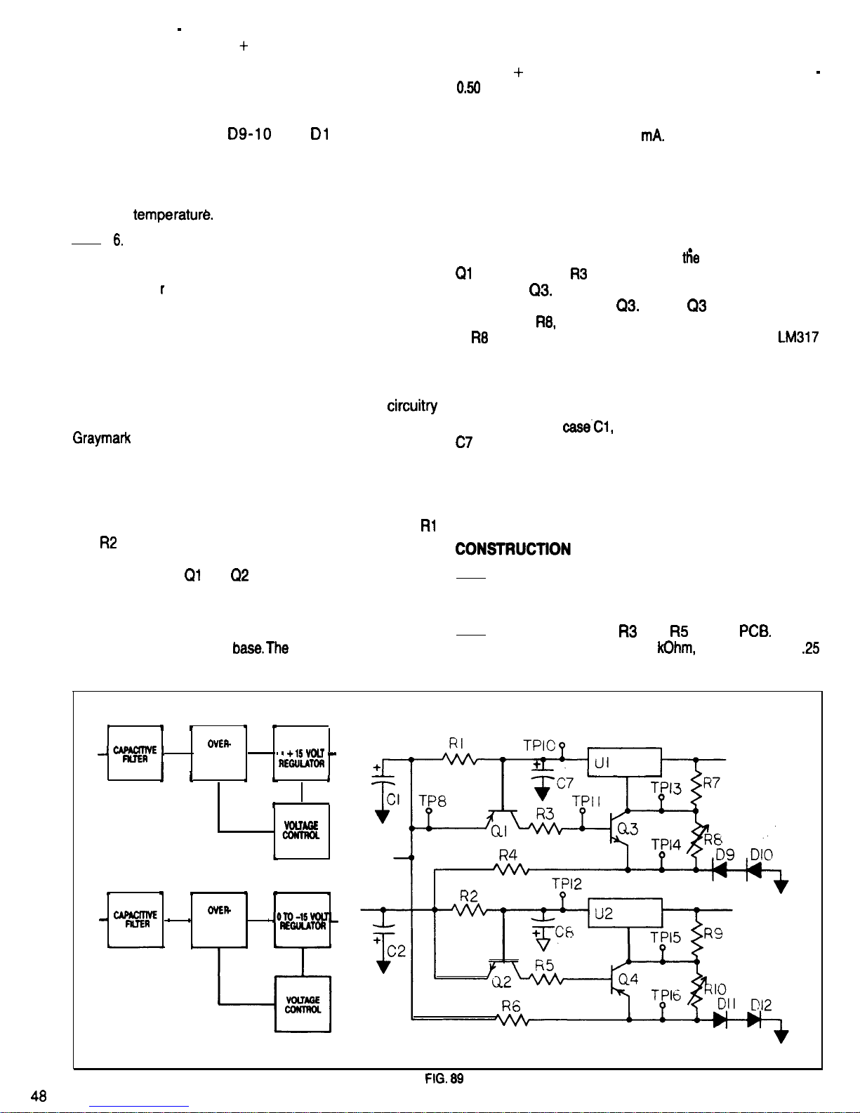
positive variable supply will have an output of
about
0.2 Volts, and the negative supply an
output of about
0.2 Volts.
This can be useful in some test situations, where
it is is helpful if a voltage can be adjusted to zero
and a little beyond. If the utmost in stability is
required from the adjustable supplies, then the
diode pairs
and
l-l 2 could be
jumpered. This would make the lowest voltage
setting obtainable 1.25 Volts, but the output
voltages would be more stable with changes in
power line voltage, load, and ambient
Turn OFF the 808 power switch, and remove its
power plug from the outlet. This completes the
ADJUSTMENT VOLTAGE EXPERIENCE. Have
you
instructor initial your Progress Guide.
PROTECTION CIRCUITRY
DISCUSSION
Figure 89 is a partial block diagram and schematic of the
808, with the external protection circuitry highlighted.
The overcurrent and over temperature protection
built into the voltage regulators that are used in Your
808 do a good job of protecting the regulators
themselves, but under some conditions over current
damage could occur to other power supply components.
With this in mind, circuitry has been designed into the 808
to give additional protection.
We have already talked about current sensing resistors
and
and used them to determine the current flowing
through the voltage regulators in tests that were done
earlier. Transistors
and
monitor the voltage drop that
occurs across these resistors.
The collector current of a transistor depends on the voltage
applied from collector to emitter, and the current flowing
between the emitter and
emitter to base current
depends primarily on the voltage applied between the
transistors base and emitter, and secondarily on the
temperature of the transistor.
At normal operating temperatures, base current starts to
flow when the voltage of the base in respect to the emitter
is about
0.50 Volts for an NPN transistor, and about
Volts for a PNP transistor. With the transistor base and
emitter leads connected across a 1 Ohm resistors, base
current begins to flow when the current through the
resistors reaches about 500
As the base current of a transistor increases, the collector
current will increase as well. A given change in the base
current of a transistor results a larger change in the
collector current. We could say that as base current
increases in a transistor, resistance between the emitter
and collector of that transistor decreases. In the positive
adjustable power supply of the 808,
collector current of
flows through
and increases the base to emitter
voltage of
This results in a drop in the emitter to
collector resistance of
Since
is connected in
parallel with
the result is the same as if the resistance
of
was reduced, and the output voltage of the
voltage regulator is reduced as well.
The voltage regulators can become unstable and cause
rapid changes or oscillations in the output voltage if there
is too much resistance or reactance between the filter
capacitor, in this
and the regulator input terminal.
is provided to prevent this oscillation.
All the polarities are reversed in the over current protection
circuit for the negative adjustable power supply, but this
circuit operates in the same-manner as the one described
above.
1.
Be sure that the 808 power plug is not connected
to a power outlet. Refer to Fig. 90 for the following
steps.
2. Mount resistor
and
on the
These
resistors are both 6.8
(blue-gray-red),
Watt. Solder the resistor leads to the PCB and
cut off any excess length. Save one of these
l
,
010
CURRENT
DETECTOR
1 1
l
.
CURRENT
DETECTOR
Page 49
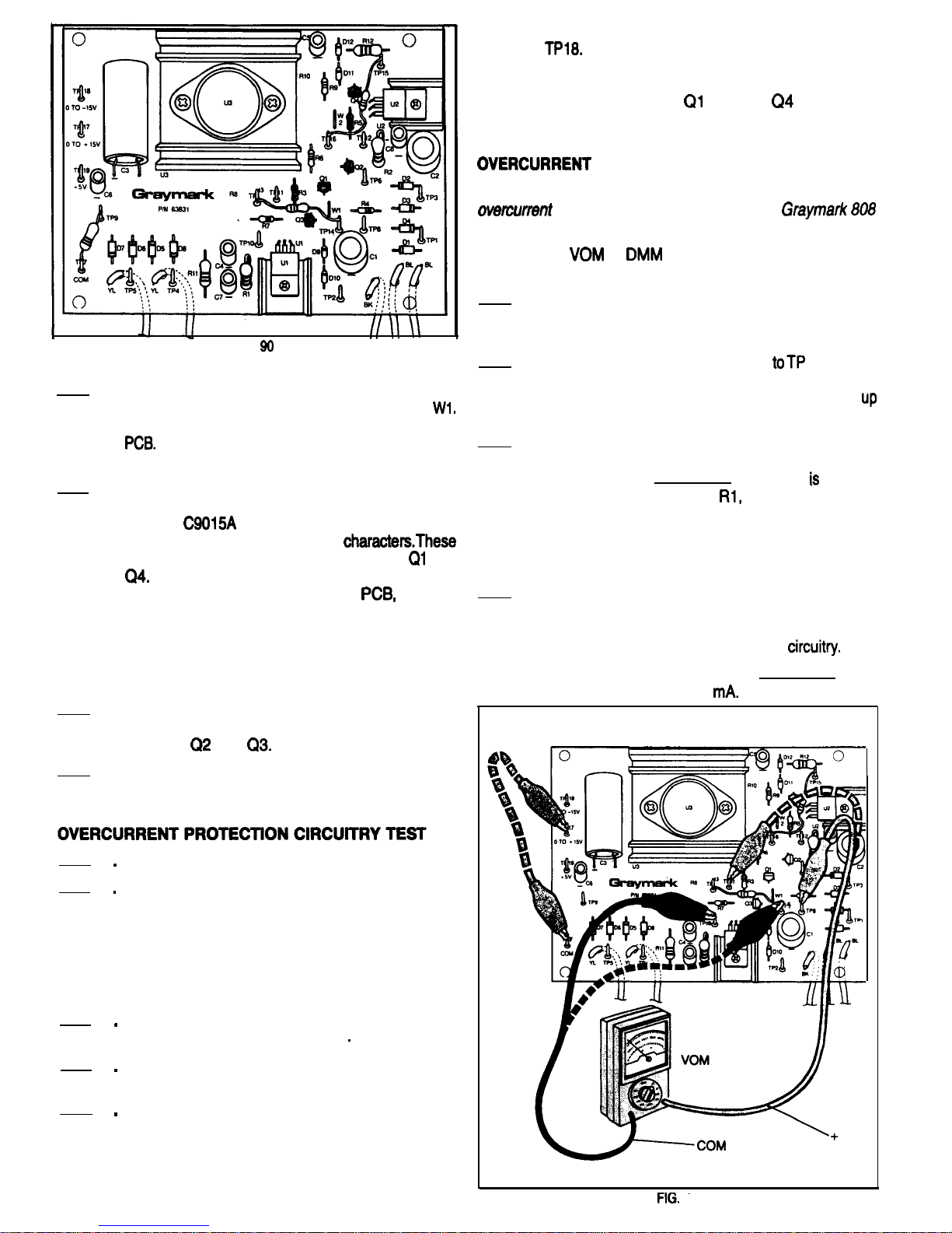
3
.
4
.
5
.
6
.
FIG.
pieces of wire for the next step.
Bend the piece of wire saved from the previous
step into a U shape and use it for jumper wire
Insert this wire from the component side of the
Solder it to the PCB and cut off any excess
length.
Locate the two transistors that are marked 9015.
There may be other numbers or letter as well,
such as
QC, but the numbers 9015 will
appear within the sequence of
are the PNP transistors and are used for
and
Spread the leads to form a triangle, and
mount these transistors on the
making
sure that they are oriented the same as the D
shaped transistor outlines that are silk screened
on the PCB. Solder the leads to the PCB, using
a heat sink as shown in Fig. 40 on each lead as
you solder it.
Repeat Step 4, using the transistors marked
9014. These are the NPN transistors and are
used for
and
This completes the construction of the external
protection circuitry. Have your instructor initial
your progress guide.
1
2
3
4
5
Connect the 808 power plug to a power outlet.
Turn the 808 power switch ON, wait 1 second
and turn it OFF touch the components that were
installed in the construction steps just
completed. If any of these components are
warm, there is something wrong. Check the PCB
and components carefully, and consult with your
instructor if necessary.
Repeat step 2, leaving the power ON for 5
seconds this time.
Repeat step 2 again, leaving the power ON for
15 seconds this time.
If none of the components heated up in the
previous steps, power up the 808 again.
Measure the DC voltage between test pointsTP7
and TP17. TP17 should be positive,and the
voltage should be between 12.7 and 15.8 Volts.
Then measure the DC voltage betweenTP7 and
TP18 should be negative and the voltage
should again be between 12.7 and 15.8 Volts. If
these voltages are not within these ranges,
check transistors
through
for proper
location and orientation. Consult with your
instructor if necessary.
PROTECTION EXPERIENCE
Purpose: To demonstrate the operation of the external
protection circuitry used in the
Power Supply
Equipment:
or
Clip Lead
1.
Be sure that the 808 power plug is not connected
to a power outlet. Refer to Fig. 91 for the following
steps.
2. Connect the positive meter lead
8 and the
negative meter lead to TP 10. Set the meter
range selector switch to a range that will read
to 1 Volt DC.
3. Connect the 808 power plug to an electrical
outlet and turn the power switch ON. What is the
meter reading?
The meter
reading
the voltage drop across
the 1 Ohm current
sensing resistor. What is the current flowing
through the resistor? Use the short cut way of
calculating the current value that was discussed
earlier in this manual.
4. Connect the clip lead to TP7 and TP17. This
provides a very low resistance load for the
positive variable power supply, and will activate
its external overcurrent protection
How
much current is flowing now?
It should be about 500
91
4
Page 50
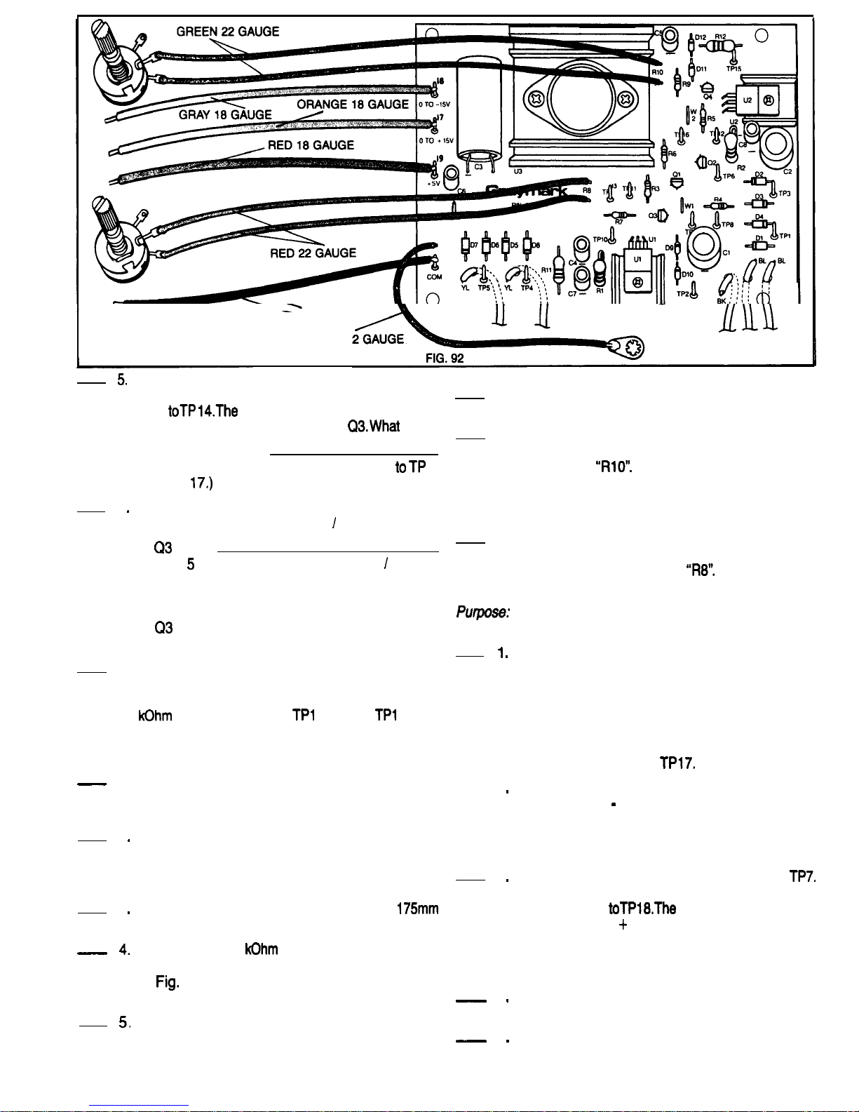
BLACK 18 GAUGE
GREEN 2
Disconnect both meter leads and reconnect the
be used.
6
positive meter lead to TP 11 and the negative
lead
meter will now read the voltage
between the emitter and base of
is the
meter reading now?
(The clip lead should still be connected
7
and TP
Remove the clip lead fromTP7 and TP 17. What
is the voltage across the base
emitter junction
of
now?
VOLTAGE CONTROL OPERATIONALTEST
To determine that the external voltage control
circuitry is working properly
In step
the voltage across the base
emitter
junction was more than 0.5 Volts, and current
was flowing from the collector to the emitter. In
this step the voltage from the base to the emitter
of
was very low, so there was almost no
current flowing from the collector to the emitter.
7. Turn OFF the 808 power switch and disconnect
the power plug from the power outlet. Remove
the test clip and meter leads. Remove the two 3.9
test resistors from
3, TP14,
5 and
TP16.
6. Repeat step 5, this time using the two red wires
and the second potentiometer.
7.
Insert the free ends of the green wires in the PCB
holes that are nearest to the silk screened
designation
Solder the wires to the PCB
and cut off any excess length. It doesn’t matter
which of the two wires goes into which of the two
holes.
8.
Repeat step 7, this time using the free ends of the
two red wires and the two holes on the PCB
closest to the designation
CONSTRUCTION
1.
2
3
Be sure that the 808 power plug is not connected
to a power outlet. Refer to Fig. 92 for the following
--
2
steps.
Cut two 200mm pieces of green 22 gauge wire
and strip 6mm of insulation from all four ends.
Twist the exposed strands of fine wire together
on each end and tin them.
3
Repeat step 2, cutting and preparing two
pieces of red 22 gauge wire.
Locate the two 5
potentiometers. Bend the
small metal tab on each potentiometer as shown
in
93 so that it won’t interfere when the
potentiometer is mounted on the cabinet top.
4
Connect and solder the two green wires
prepared in step 2 to one of the potentiometers
5
as shown in Fig. 93. It is important that the
correct solder terminals of the variable resistors
During this test be careful not to let the terminals
of the potentiometers touch the PCB or any of the
components. Rotate the control shafts of both
potentiometers to the full counter clockwise
position. Adjust the range selector of your VOM
or DMM to measure up to 20 Volts DC. Connect
the negative meter lead to TP7. Connect the
positive meter lead to
Power up the 808. The voltmeter should read
between 0 and
0.3 Volts. Rotate the Shaft of the
potentiometer connected to the red wires to the
full clockwise position.The voltmeter should now
read between 15.5 and 20 Volts.
Remove the voltmeter leads fromTP17 and
Reconnect the positive meter lead toTP7 and the
Negative lead
voltmeter should read
between 0 and
0.3 Volts. Rotate the shaft of
the potentiometer connected to the green wires
to the full clockwise position. The meter should
now read between 15.5 and 20 Volts.
Turn OFF the 808 power switch and disconnect
the power plug from the power outlet.
This completes the VOLTAGE CONTROL
OPERATIONAL TEST Have your instructor
initial your progress guide.
50
Page 51
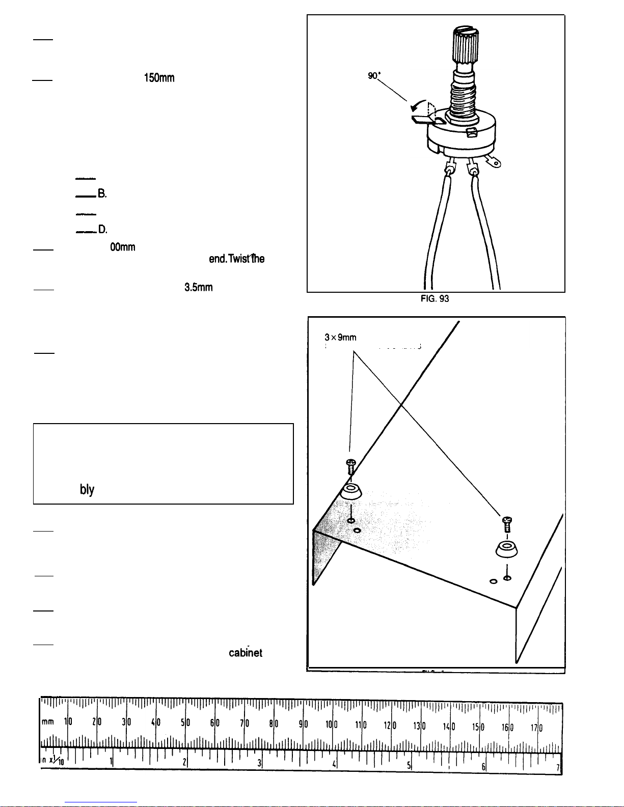
FINAL PCB ASSEMBLY
1. Be sure that the 808 power plug is NOT
connected to a power outlet. Refer to Fig. 92 for
the following steps.
2.
Locate the four
lengths of 18 gauge wire.
strip 6mm of insulation from each end of each of
the four wires. Twist the fine strands of exposed
wire on each of the ends together and tin them.
Form one of the tinned ends of each of the wires
into a hook shape with a long nose pliers.
Connect and solder these hooked wire ends to
the following test points on the PCB.
A. The black wire to TP 7.
The red wire to TP 19.
C. The orange wire to TP 17.
The gray wire to TP 18.
3.
Cut a 1
piece of green 22 gauge wire. Strip
6mm of insulation from each
small
strands of wire together, and tin both ends.
4.
Connect and solder the
solder lug to one
end of the green wire that you prepared in the
previous step. Connect and solder the other end
of this wire to the PCB. Use the unmarked hole
near TP 7. Cut off any excess wire.
5. This completes the FINAL PCB ASSEMBLY.
Have your instructor initial your progress guide.
CABINET ASSEMBLY
CAUTION!
Be sure that the AC Cord is NOT plugged
into an electrical outlet during this Cabinet
Assem
Section.
1.
Mount two rubber feet to one end of the cabinet
bottom, using two 3 x 8mm self-tapping screws.
Refer to Fig. 94.
2.
Repeat the previous step for the other end of the
cabinet bottom.
3. Remove the protective plastic from the
breadboard.
4. Place the cabinet top face up on your work
BEND
TAB
SELF-TAPPING SCREWS
FIG. 94
surface, so the printing on the
top is
readable.
Page 52
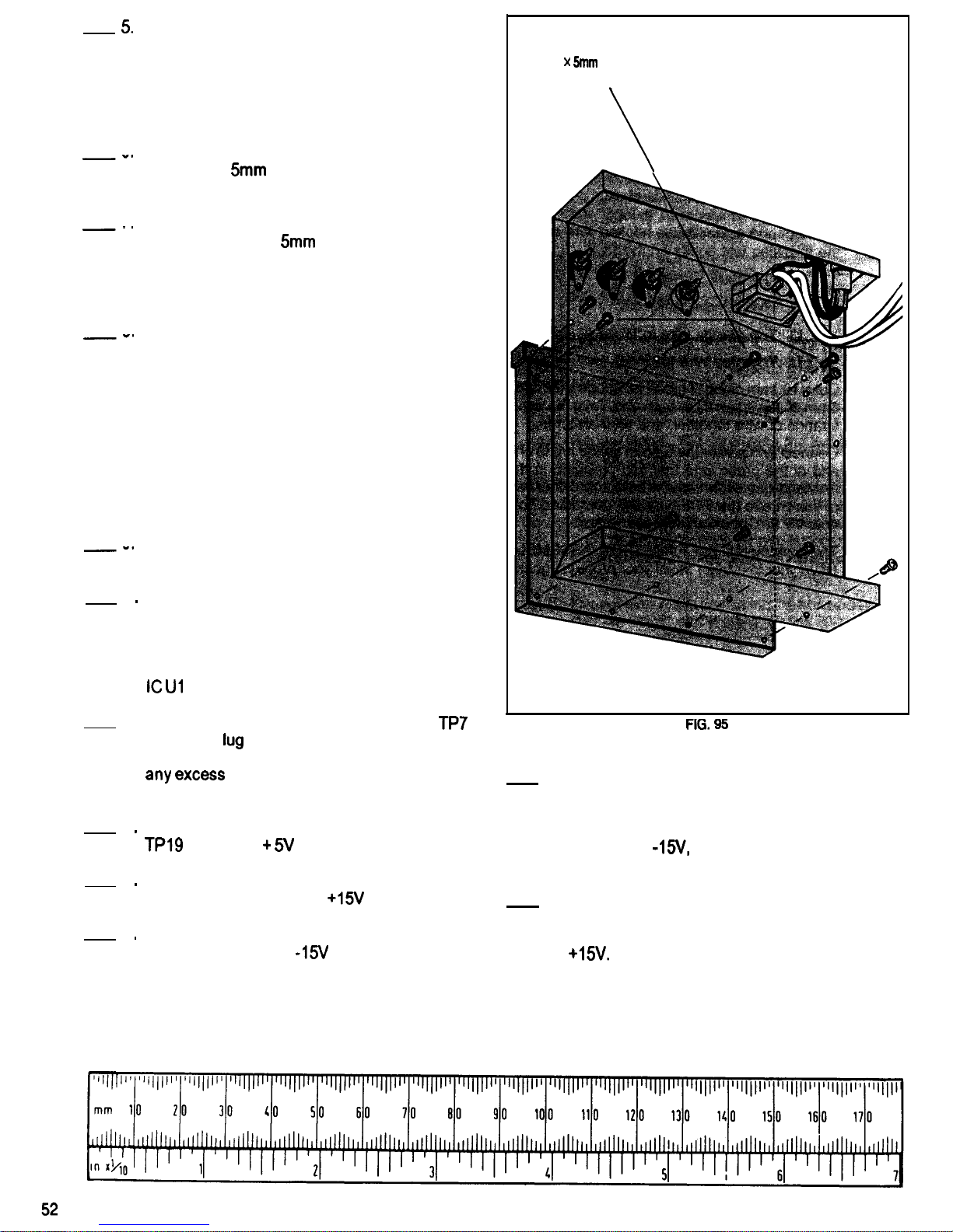
Position the breadboard on the cabinet top, so
the printing on the breadboard is readable. While
holding the breadboard in place, turn the cabinet
top over.
Refer to Fig. 95 for the following steps.
6
7
Refer to
8
9
10
11.
12
13
14
Attach the breadboard to the cabinet top using
eight 2.6 x
self-tapping screws. Do not
over tighten the screws.
Attach the breadboard bus strip to the cabinet
top using two 2.6 x
self-tapping screws. Do
not over tighten the screws.
Fig. 96 for the following steps.’
Position the transformer so the side with the two
white wires is next to the cabinet side. Mount the
transformer to the cabinet bottom using two 3 x
8mm machine screws, two 3mm flat washers,
two 3mm lockwashers, and two 3mm nuts. Place
the solder lug which is attached to the green
wire from the PCB between the transformer and
the cabinet bottom as shown in Fig. 96. This
wire provides an electrical connection between
Common (ground) on the PCB and the metal
cabinet.
Unscrew and remove the four screws which are
holding the standoffs at each corner of the PCB.
Using the screws, standoffs and nuts removed in
the previous step, mount the PCB to the cabinet
bottom. Place four 3mm lockwashers between
the top of the PCB and the two 3mm nuts and
the two long standoffs. Position the PCB so that
Ul is next to the transformer.
Connect and solder the black wire from
to
the solder
on the black binding post which
was installed on the cabinet top earlier, Cut off
wire that sticks out beyond the
solder lug.
Repeat Step 11, connecting the red wire from
to the red
5V binding post.
2.6 SELF-TAPPING SCREWS
(10 PLACES)
15. Place a 7mm lo&washer over the threaded
bushing of the potentiometer which is connected
to the PCB with two green wires. Mount the
potentiometer in the hole in the cabinet top
marked 0 to
using a 7mm flat washer and
hex nut.
Repeat Step 11, connecting the orange wire
from TP17 to the red 0 to
binding post.
16. Repeat the previous step using the
Repeat Step 11, connecting the gray wire from
potentiometer connected to the PCB with two
TP18 to the red 0 to -15V binding post.
red wires, mounting it in the hole marked 0 to
Page 53
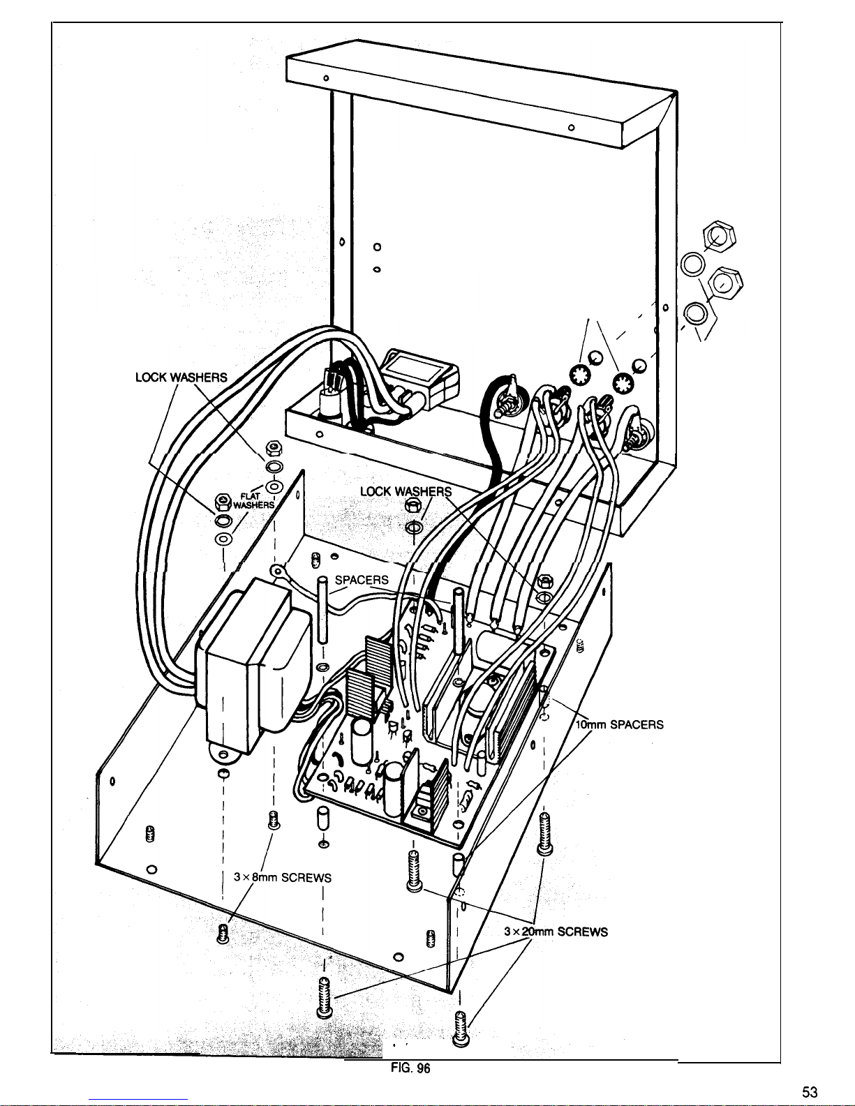
0
0
LOCK
WASHERS /
’
FLAT
WASHERS
Page 54
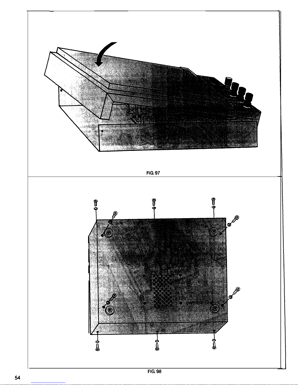
Page 55
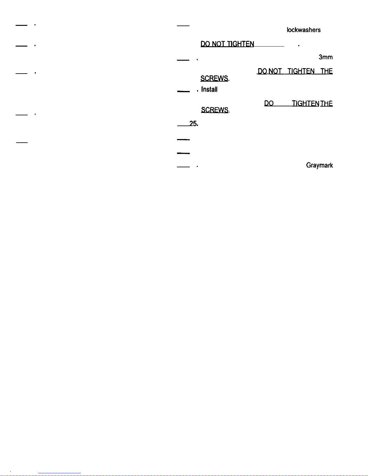
Refer to Fig. 97 for the following steps.
Refer to Fig. 98 for the following steps.
17
Place the cabinet bottom on your work surface
22,
as shown in Fig. 97.
18
Make sure that all four brackets are lined up
perpendicular with ‘the cabinet top before
proceeding.
23
19
Hold the cabinet top so that it can be folded onto
the cabinet bottom like a hinge. Carefully
position all wires so that they will not be pinched
between any metal or other parts when the
24
cabinet top is assembled to the cabinet bottom.
20
Gently lower the cabinet top onto the cabinet
bottom. Observe the wires to be sure they are
not pinched between any parts.
21. Once the cabinet top is positioned firmly onto the
26
l
cabinet bottom, hold the two cabinet halves
tightly together while you turn the unit over.
27
l
Continue to hold the cabinet tightly together.
28
While holding the cabinet together, install four
(4) 3 x 8mm screws with 3mm
into
the four (4) holes in the bottom of the cabinet-
THESC-
Install three (3) 3 x 8mm screws with 3mm
lockwashers into the three holes on the left side
of the cabinet.
three (3) 3 x 8mm screws with 3mm
lockwashers into the three (3) holes on the left
side of the cabinet.
NOT
Tighten the screws installed in Step 22.
Tighten the screws installed in Step 23.
Tighten the screws installed in Step 24.
This completes construction of your
Model 808 Triple Power Supply/Bread board.
55
Page 56
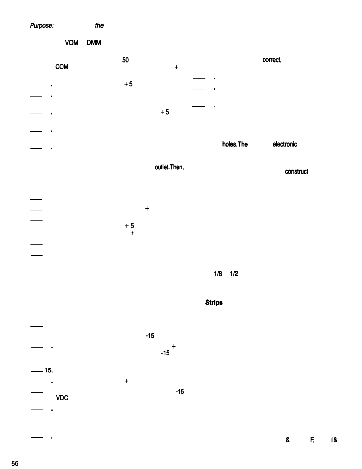
FINAL TEST
To verify that
three power supplies work
properly after cabinet assembly
Equipment:
or
1
l
2
3
4
5
6
7.
8
.
9
.
10.
11
.
12.
13.
14
16
17.
18
19
.
20
50 Ohm 5 Watt Resistor
Connect one end of the
Ohm resistor to the
terminal. Connect the other end to the
5
VDC terminal.
Adjust the meter to read
VDC.
Connect the negative meter lead to the COM
terminal.
Connect the positive meter lead to the VDC
terminal.
Connect the 808 power plug to an electrical
outlet and turn the power switch ON.
The voltmeter should read between 4.7 and 5.3
Volts. If the voltage is correct, proceed to the next
step. If it is not correct, STOP, turn power OFF
and remove the power plug from the
check the resistor and meter connections. If all
connections are correct, you may have pinched
or broken a wire during the cabinet assembly.
Turn the power switch OFF
Adjust the DC Voltmeter to read
15 VDC.
Disconnect the resistor lead and the positive
meter lead from the
VDC terminal.
Reconnect both to the 0 to
15 VDC terminal.
Turn the power switch ON.
Monitor the voltage while turning the adjustment
potentiometer using a small screwdriver. You
should be able to adjust the supply between 0
and 15 Volts. If the voltage is correct, proceed to
the next step. If it is not correct, STOP, turn power
OFF and remove the power plug from the outlet.
Then check the resistor and meter connections.
If all connections are correct, you may have
pinched or broken a wire during the cabinet
assembly.
Turn the power switch OFF
Adjust the DC Voltmeter to read
VDC.
Disconnect the resistor lead from the 0 to
15
VDC terminal. Reconnect it to the 0 to
VDC
terminal.
Disconnect both meter leads.
Adjust the meter to read
15 VDC.
Connect the negative meter lead to the 0 to
terminal.
Connect the positive meter lead to the COM
terminal.
Turn the power switch ON.
Monitor the voltage while turning the adjustment
potentiometer. You should be able to adjust the
supply between 0 and 15 Volts. You should be
21
22
23
able to adjust the supply between 0 and 15 Volts.
If the voltage is correct, proceed to the next step.
if it is not correct, STOP, turn power OFF and
remove the power plug from the outlet. Then
check the resistor and meter wnnections. If all
wnnections are
you may have pinched
or broken a wire during the cabinet assembly.
Turn the power switch OFF
Disconnect the voltmeter and resistor from the
Model 808.
This completes the Final Test.
OPERATION
The Breadboard portion of your Model 808 is populated
with 2,420
leads of
wmponents such
as integrated circuits, transistors, resistors and capacitors,
as well as wires, can be inserted into these holes By
inserting electronic components and wires into the
Breadboard, you can design and
experimental
(prototype) circuits. Before you can use the Breadboard,
however, you must understand how the 2,420 holes are
interwnnected.
The Breadboard is comprised of eight sections, five bus
strip sections and threecomponent sections, as shown in
Fig 99. The bus strips are used to distribute or “bus”
power and electronic signals to different areas of the
Breadboard. The component sections are where the
electronic components are mounted.
Various wire sizes can be accommodated by the
Breadboard, as well as the following component leads:
SIP and DIP Integrated Circuits
to
Watt Resistors
Most Capacitors
Most Small Transistors
Bus
Each of the five bus strips wntains four segments of 25
holes each. Each segment is identified by a blue or red
stripe printed next to the segment.The 25 holes which are
next to each stripe are connected together, so that a wire
or component lead inserted into any of the 25 holes will be
connected to any wire or wmponent which is inserted into
any of the remaining 24 holes in that segment.
Component Sections
Each of the three component sections contains 128
segments of five holes each.The segments are horizontal
rows, and each segment is identified by a number (1 to 64)
printed next to the segment.The five holes in the row next
to each number are wnnected together, so that a wire or
component lead inserted into any of the five holes will be
connected to any wire or wmponent which is inserted into
any of the remaining four holes in that segment.
In each wmponent section, for reference only, the columns
are identified by letters A, B, C, D
E, and
G, H, J.
A portion of the Breadboard is shown in Fig. 104 to illustrate
Page 57
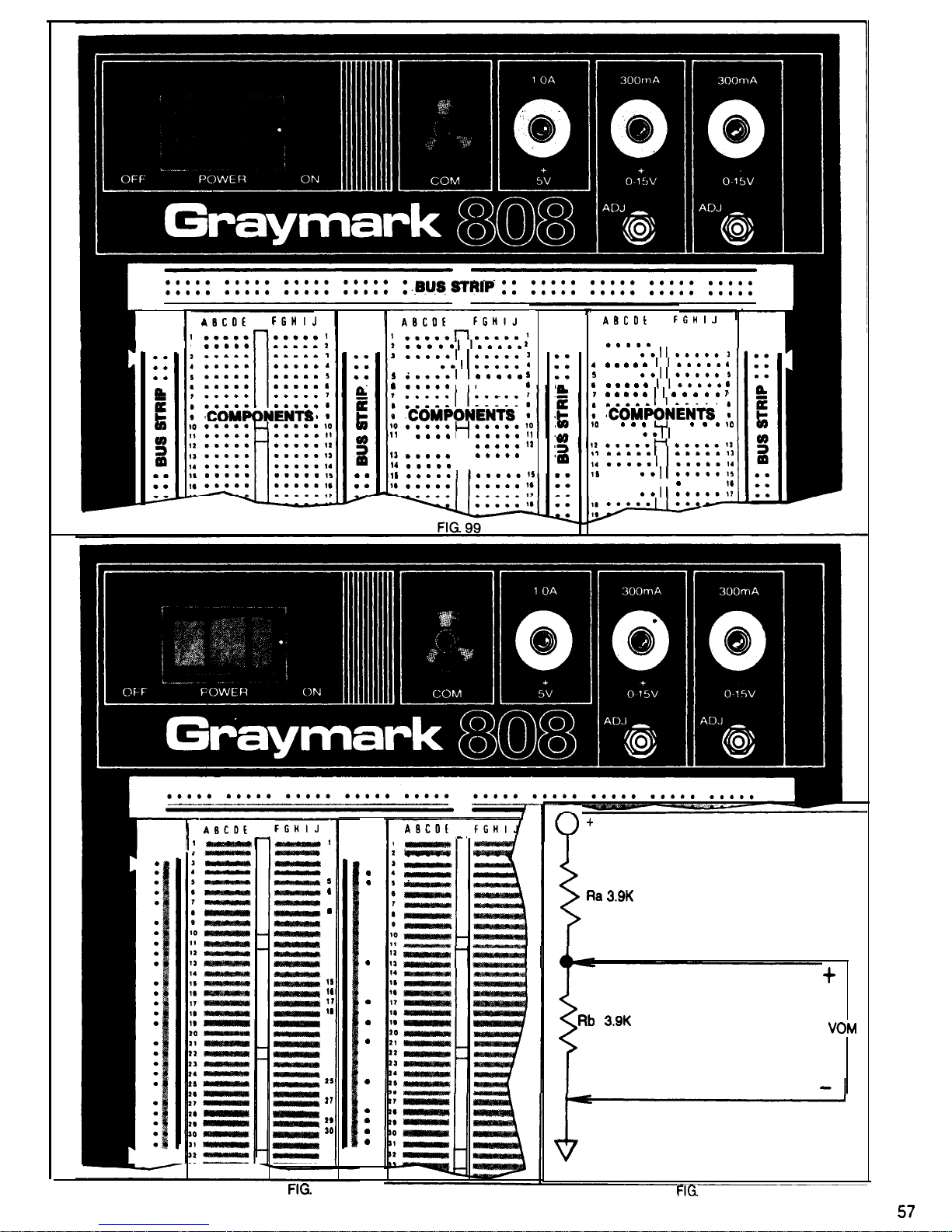
1
l o***
l oooo'
2
rl
. . ...2
2
3
. . .
. . .
4
. . .
. . . . .
I I
. . . . .
l l a a a
l l
11
. . .
l . . . . 11
l
H
12
l mo*m
13
. . .
I I
l . l . . 14
19 . . . . .
I I
a.. .
17
. . .
5 VOLTS
2
3
4
7
9
10
11
12
13
14
19
20
21
22
23
24
29
29
31
32
33
l
l
l
l
l
l
l
l
l
l
l
l
l
l
100
101
L
Page 58
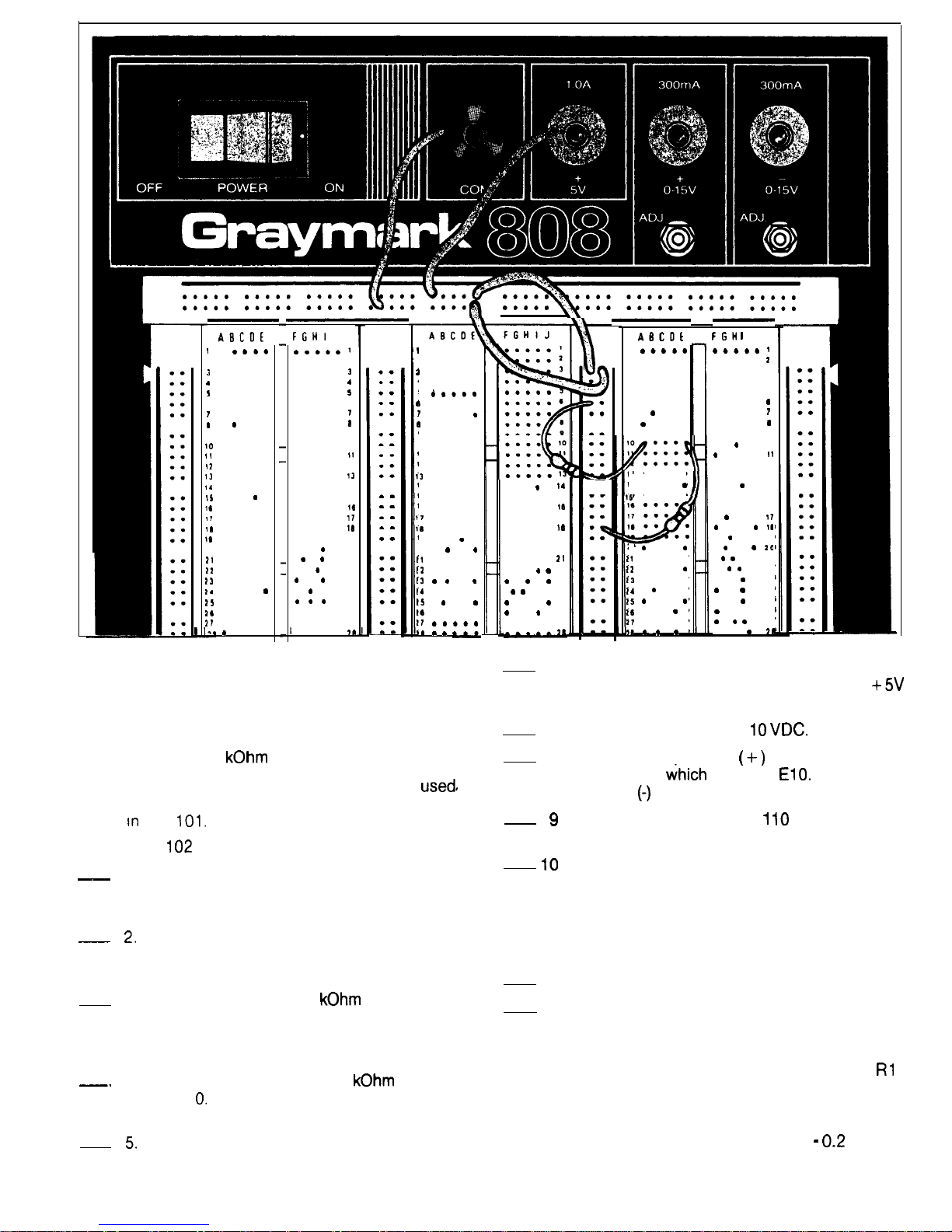
l
2
l l l l l
l . l l l
l l l l l
l l l l l
b
l l l l l
l l l l l
l
l l l
9
l l l l l
l l l l l
l l l l l
l l l l l
l l l l l
l l l l l
l l l
l
l l l l l
l oeee
l l l l l
l l l l l
20 l l l l l
l l l l l
l eeee
l eeee
l l l l
l eeee
l l l l l
l l l l
J
l eeee2
l eeee
l eeee
l eeee
l eeee b
l eeee
l eeee
l eeee 9
l l l l l 10
l l l l l
l l l l l 12
l l l l l
l l l l l 14
l l l l l 15
l l l l l
l l l l l
l l l l l
l l l l l 19
l l l l
20
l
l l
21
l l l
l 22
l l l
23
l l
l l 24
l
l
25
l l l l l 2b
l l l l l 27
l l l l l
l l l l l
2
l l l l l
l l l l l
4
l l l l l
5
l l l l l
l l l l
l eeee
9
l l l l l
10 l l l l l
11
l l l l l
12
l l l l l
l eeee
14 l eeee
15 l eeee
lb l l l l l
l l l l l
19 l l
l l
20
l l l
l eeoo
l eeee
l l
l
l l
l l l l l
FIG. 102
l l l
l
l l l l l 15
l l l l l
l eoe*l7
l l l l l
l l l l l 19
l l l l l 20
l l l l l
l l l
22
23
l l l 24
l 29
l l l l l 27
1
2
l eee*
3
l l l l l
4
l l l l l
5
l l l l l
b
l l l l l
7
l
l l l
I
9
l l l l l
13
l eeee
14
l l l l
l eeee
20
l l l
l eeee
l l l l
l l l l l
l
l l l
l l l
l l l
l
l l a l l
l
l
J
l eeee
l eeee 3
l e*e* 4
l eeee 5
l eeee
l eeee
l eo*e
l eeee 9
l l l
l 10
l l l l
l ee*e 12
l l l l l 13
l l l l
14
l l l l l 15
l l l l l lb
l
l l l I?
l l l
l l
l l 19
l
l l 0
l l l 21
l l l 22
l l l l
23
l l l
24
l l l l
25
l l
0 27
l l l
l 28
the interconnections in both the bus strip and the
component sections.
Sample Circuit
Equipment: VOM or DMM
Two 3.9
Resistors
To demonstrate how the Breadboard can be
to
construct circuits, you can build the voltage divider circuit
shown
Fig.
Refer to Fig.
for the following steps.
1.
3.
4.
Connect one end of a wire to the COM terminal.
Insert the other end of the wire into the hole in the
upper bus strip as shown.
Insert one end of a wire into the hole in the upper
bus strip as shown. Insert the other end into the
hole in the vertical bus strip as shown.
Insert one end of a 3.9
resistor into the
hole in the vertical bus strip as shown. Insert the
other end in hole Al 0 in the center component
section.
Insert one end of another 3.9
resistor into
hole El
Insert the other end into the hole in the
vertical bus strip as shown.
Insert one end of a wire into the hole in the
vertical bus strip as shown. Insert the other end
into the hole in the upper bus strip as shown.
6. Insert one end of a wire into the upper bus strip
as shown. Connect the other end to the
terminal.
7. Adjust the meter to read
8. Connect the positive meter lead to the
resistor lead
is in hole
Connect the
negative
meter lead to the COM terminal.
Plug the Model 808 into a VAC outlet and
turn the Power ON.
Read the meter. It should read approximately 2.5
VDC, showing that the voltage divider circuit is
operating as expected, you know that the circuit
which you built on the Breadboard is connected
in accordance with the schematic in Fig. 101.
11. Turn the Power OFF and unplug the Model 808.
12. Remove the meter and all wires and resistors
from the Breadboard.
NOTE: Due to the nature of the design, when the Positive
and Negative Variable Voltage control pots (R8 and
0)
are set to the full counter-clockwise position (for minimum
output), the output voltage level can go past zero and
produce an output in the opposite polarity. Levels upwards of one to two hundred millivolts (0.1 Volts) of
reversed polarity are possible, and can adversely affect
some semiconductor devices, Make sure that you have
58
Page 59
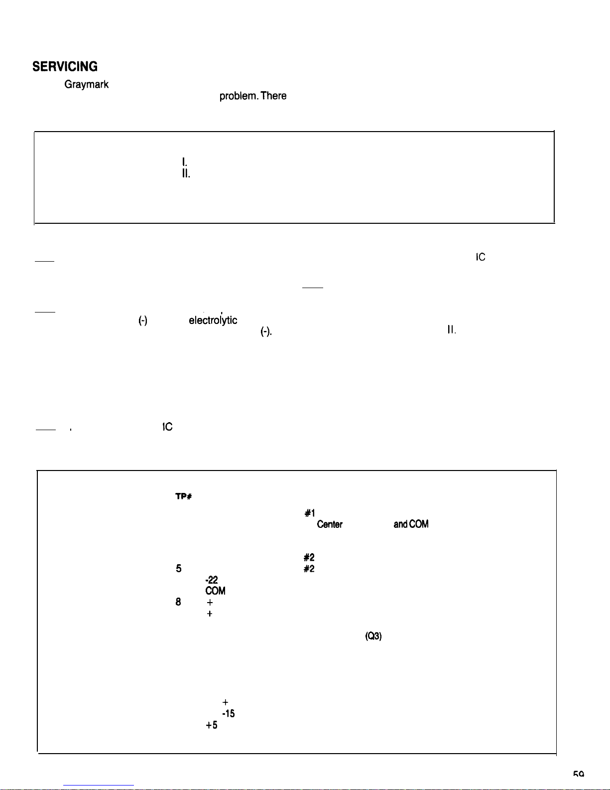
the two Variable Voltage Outputs set to the desired level
before connecting them to the breadboarded circuit, and
do not randomly adjust the control pots during operating.
If your
project does not operate correctly, the
following steps will help you to isolate the
are three basic steps to follow when servicing any
electronic device.
Isolate the defective section.
Isolate the defective component or connection.
Ill. Repair or replace the defective component or
connection.
Check off each step as you proceed.
1. Check ALL solder connections. Poorly soldered
for their part numbers. Each
must be in the
connections should be reheated to form good
correct location.
joints. Refer to the HOW TO SOLDER section for
examples of good and poor solder connections.
4. If the above procedures fail to locate the
problem, performing the experiences located
2. Check the placement of ALL components. Make
sure that the
leads of
capacitors
are going into the PCB holes marked
Be
certain that you have installed the proper
capacitors in the right locations. It is easy to get
confused by the numbers on capacitors. Check
that all resistors have been installed in their
proper locations. Resistor values can be
determined by the RESISTOR COLOR CODE
section.
throughout the manual will be helpful in locating
the problem, especially if you built the Power
Supply using Mode
These experiences
demonstrate how the various sections of your
Power Supply operate. If you find results that
differ greatly from those described, you will know
where to look for trouble in your Power Supply.
Be sure that each
has been installed in the
proper location. Ul and U2 look similar, except
3
TEST POINT DESCRIPTIONS
DESCRIPTION
1
2
Transformer Secondary
Start (Blue)
Transformer Secondary #1
Tap (Black)
(Ground)
3
4
6
7
9
10
11
12
13
14
15
16
17
18
19
Transformer Secondary #1 Finish (Blue)
Transformer Secondary
Start (Yellow)
Transformer Secondary
Finish (Yellow)
Volts, Unregulated
(Ground)
22 Volts, Unregulated
11 Volts, Unregulated
Positive Regulator Input Terminal
Overcurrent Protection Transistor Base
Negative Voltage Regulator Input Terminal
Positive Voltage Regulator Adjust Terminal
Minus 1.4 Volt Voltage Control Bias
Negative Voltage Regulator Input Terminal
Positive 1.4 Volt Voltage Control Bias
0 to
15 Volt Output, Regulated
0 to
Volt Output, Regulated
Volt Output, Regulated
Page 60
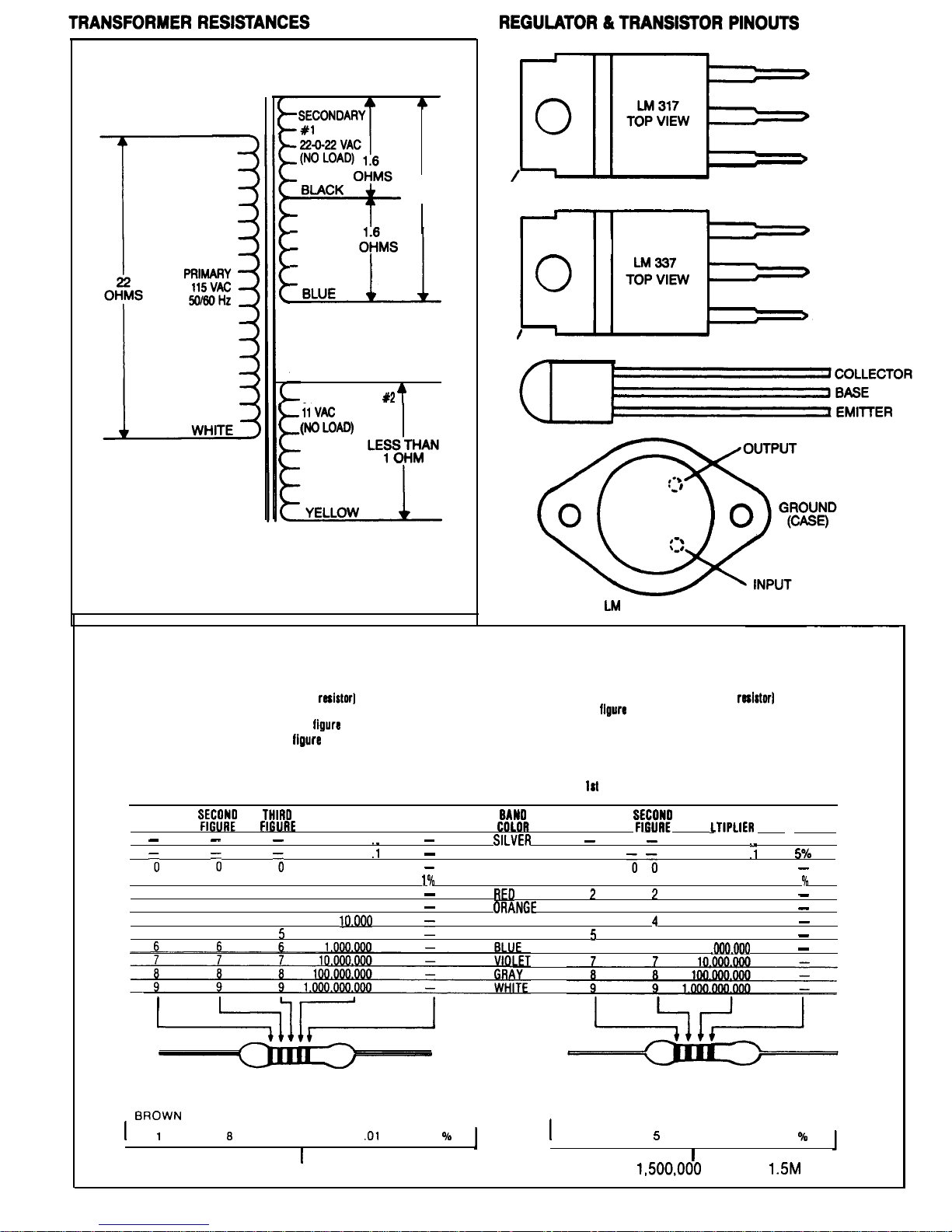
WHITE
BLUE
3.2
OHMS
YELLOW
SECONDARY
(NO LOAD)
LESS THAN
1 OHM
YELLOW
Tl
POWER TRANSFORMER SPECIFICATIONS
TAB CONNECTED TO OUTPUT
TAB CONNECTED TO INPUT
INPUT
OUTPUT
ADJUST
OUTPUT
INPUT
ADJUST
309 TOP VIEW
RESISTOR COLOR CODE
Your kit contains precision resistors which may use two types of color code: a four band code and a five band code.
FIVE BAND COLOR CODE
l First color (color nearest the end of the
represents the first
figure in the resistor value.
l Second color represents the second
in the resistor value.
l Third color represents the third
in the resistor value.
l Fourth color represents the multiplier of the first three figures.
l Fifth color represents the resistor tolerance.
1st
2nd
3rd
4th
5th
COLOR COLOR
COLOR COLOR
COLOR
FIRST
FIGURE FIGURE
MULTIPLIER TOLERANCE
01
1
1 1
1
10
2 2
2
100
3 3 3
1,000
4 4 4
5 5 5
100,000
FOUR BAND COLOR COOE
l First color (color nearest the end of the
represents
the first
in the resistor value.
l Second color represents the second figure in the resistor
value.
l Third color represents the multiplier of the first two figures.
l Fourth color represents the resistor tolerance.
2nd
3rd
4th
COLOR COLOR COLOR
COLOR
FIRST
FIGURE
MU
TOLERANCE
01
10%
GOLD
BLACK
1
BROWN
1 1
10
1
100
3 3
1 .ooo
YELLOW
4
10.000
GREEN
100.000
6 6
1
EXAMPLES
GRAY
YELLOW SILVER BROWN BROWN GREEN GREEN BROWN
1
1
100,000
1
equals 1.84 ohms equals
ohms or
60
Page 61
This project has afforded you the opportunity of expanding
your knowledge of electronic& and electronic devices
have learned, and the amount of knowledge you have
acquired from building this project. The theory and skills
through experiments and related technical information.
which were covered are:
You will probably be surprised at the number of skills you
THEORY
Transformers
Rectification
Center-Tap Rectification
Bridge Rectification
Bridge With Center-Tap Rectification
Capacitive Filters
Unregulated Power Supplies
Fixed Voltage Regulators
Variable Voltage Regulators
Overcurrent Protection
Electronic Component Identification
Schematic Symbol identification
Reading Schematic Diagrams
Reading Block Diagrams
Reading Resistor Color Code
Test Equipment Use
Soldering
Hand Tool Use
SPECIFICATIONS
POWER SOURCE: 110 VAC
POWER
VDC, 1 Amp
0 to
15 VDC, 300
0 to
-15
300
INTEGRATED CIRCUITS:
3
TRANSISTORS:
4
DIODES:
12
HOW TO ORDER REPLACEMENT PARTS
REPAIR POLICY
If you require a part, follow the instructions below.
If your
project does not operate properly, and
ment parts will be shipped subject to the warranty terms.
you have completed the steps outlined in SERVICING, you
Do not return the original component unless requested.
may return the project to
for inspection and
The Factory Warranty does not cover components
repair.
aged through carelessness or incorrect assembly. Mail
your request for replacement parts to Graymark.
1
Enclose the following:
2
1. Your name and mailing address.
2. Date kit was purchased.
3. Part number and description (as shown on Parts List)
3
4. If the part is not covered by warranty, you must also:
A
A
B
.
C
.
D
Carefully pack the completed project so it
not
be damaged in shipment.
Enclose a letter explaining the problem. Include
your name, address and phone number.
Allow 4 weeks for repair and return.
Send your kit to:
INTERNATIONAL, INC.
Show replacement price from Parts List.
Add $1
for postage
handling.
If you are a
resident, add
on
purchase price.
Tustin, CA 92680
Enclose a money order or check for the full amount.
Sorry, COD not accepted.
61
Page 62
FACTORY WARRANTY
international, inc. warrants that each project was
complete and ready to assemble at the time of shipment.
shortage claims must be made within
days from
ceipt of goods representing each project.
warrants that, for a period of ninety (90) days from date of purchase, all merchandise is free of defects and workmanship,
under normal conditions of use and service. The
of
under this warranty is limited to repair or
placement of those parts upon verification that they are de-
fective in this
does not in-
clude labor required to service or repair any project.
This warranty is completely void and
not
replace, or service any project or parts thereof on
which acid core
paste
or corrosive solders have
been used in assembling the project. Any modification of
the project will void the warranty.
This warranty is extended solely to the original buyer and
only to the extent above expressed. No dealer or agent is
authorized to make any other or additional guarantee or
warranty.
no event shall
be liable for any anticipated profits, consequential damage, loss of time, or other
losses incurred by
the buyer in connection with the
OTHER
KITS
There are many other
electronic projects
will enjoy building. Send your name and address to:
BOX 2015,
CA 92681
for your personal copy of Graymark’s latest catalog
includes:
ROBOTS
RADIOS
TOOLS
STROBE LIGHT
ELECTRONIC ACCESSORIES
POWER SUPPLIES
An extensive selection of low-cost KOMPONENT KITS is
also described in the catalog.
62
 Loading...