

Page 1
Instruction Manual
071-0547-01
FIRST PRINTING: JANUARY 1999
REVISED PRINTING: APRIL 1999
8914
DUAL AES/EBU DELAY DISTRIBUTION AMPLIFIER
Page 2

Contacting Grass Valley Group
Region Voice Fax Address Web Site
North America (800) 547-8949
530-478-4148
Pacific Operations +852-2585-6688
Support: 852-2585-6579
U.K., Europe, Asia, Middle East +44 1753 218 777 +44 1753 218 757
France +33 1 45 29 73 00
Germany +49 221 1791 234 +49 221 1791 235
Copyright © Grass Valley Group. All rights reserved.
This document may not be copied, in whole or in part, or otherwise reproduced, except as specifically
permitted under U.S. copyright law, without the prior written consent of Grass Valley Group, P.O. Box
599000, Nevada City, CA 95959-7900 USA. GRASS VALLEY GROUP is a registered trademark and
Grass Valley is a trademark of Grass Valley Group. All registered trademarks and trademarks are property of their respective holders. Grass Valley Group products are covered by U.S. and foreign patents,
issued and pending. Product options and specifications subject to change without notice. The information in this manual is furnished for informational use only, is subject to change without notice, and
should not be construed as a commitment by Grass Valley Group. Grass Valley Group assumes no responsibility or liability for any errors or inaccuracies that may appear in this publication.
(530) 478-3347 Grass Valley Group
+852-2802-2996
P.O. Box 599000
Nevada City, CA 95959-7900
USA
www.grassvalleygroup.com
Page 3

Contents
About This Manual . . . . . . . . . . . . . . . . . . . . . . . . . . . . . . . . . . . . . . . . . . . . . . . . . . . . . v
8914 Dual AES/EBU Delay Distribution Amplifier
Introduction . . . . . . . . . . . . . . . . . . . . . . . . . . . . . . . . . . . . . . . . . . . . . . . . . . . . . . . . . . . 1
Module Installation. . . . . . . . . . . . . . . . . . . . . . . . . . . . . . . . . . . . . . . . . . . . . . . . . . . . . 2
Cabling . . . . . . . . . . . . . . . . . . . . . . . . . . . . . . . . . . . . . . . . . . . . . . . . . . . . . . . . . . . . . 3
Inputs . . . . . . . . . . . . . . . . . . . . . . . . . . . . . . . . . . . . . . . . . . . . . . . . . . . . . . . . . . . . . 3
Outputs . . . . . . . . . . . . . . . . . . . . . . . . . . . . . . . . . . . . . . . . . . . . . . . . . . . . . . . . . . . 4
Adjustments, Testpoints, and Indicators . . . . . . . . . . . . . . . . . . . . . . . . . . . . . . . . . . . 4
Delay Adjustments . . . . . . . . . . . . . . . . . . . . . . . . . . . . . . . . . . . . . . . . . . . . . . . . . . . 5
48 KHz Input Signal Example . . . . . . . . . . . . . . . . . . . . . . . . . . . . . . . . . . . . . . . . 5
Specifications . . . . . . . . . . . . . . . . . . . . . . . . . . . . . . . . . . . . . . . . . . . . . . . . . . . . . . . . . . 6
Service . . . . . . . . . . . . . . . . . . . . . . . . . . . . . . . . . . . . . . . . . . . . . . . . . . . . . . . . . . . . . . . . 7
Functional Description . . . . . . . . . . . . . . . . . . . . . . . . . . . . . . . . . . . . . . . . . . . . . . . . . . 8
Receive Circuit . . . . . . . . . . . . . . . . . . . . . . . . . . . . . . . . . . . . . . . . . . . . . . . . . . . . . . . 8
FPGA . . . . . . . . . . . . . . . . . . . . . . . . . . . . . . . . . . . . . . . . . . . . . . . . . . . . . . . . . . . . . . . 8
FIFO Circuits . . . . . . . . . . . . . . . . . . . . . . . . . . . . . . . . . . . . . . . . . . . . . . . . . . . . . . . . 9
Line Drivers . . . . . . . . . . . . . . . . . . . . . . . . . . . . . . . . . . . . . . . . . . . . . . . . . . . . . . . . . 9
Frequency Lock LEDs . . . . . . . . . . . . . . . . . . . . . . . . . . . . . . . . . . . . . . . . . . . . . . . . . 9
Index
8914 Instruction Manual iii
Page 4

Contents
iv 8914 Instruction Manual
Page 5

Preface
About This Manual
This manual describes the features of a specific module of the 8900 Series
Distribution Amplifier family. As part of this module family, it is subject to
Safety and Regulatory Compliance described in the 8900 Series frame and
power supply documentation (see the
8900 Series User’s Guide ).
8914 Instruction Manual v
Page 6

Preface
vi 8914 Instruction Manual
Page 7

8914 Dual AES/EBU Delay
Distribution Amplifier
Introduction
As the transition to digital video and audio accelerates, there is an
increased need to delay the audio associated with broadcast video. This is
due to the relatively large processing times associated with DVEs and
switchers. The 8914 provides a low cost and easy-to-use solution to the lip
sync errors associated with these large delays. Minimizing space requirements, the 8914 provides two fully controllable delay paths on a single
board, allowing up to 20 delays (ten modules) in a two rack unit frame. If
instead of two delays you require more distribution, the first channel can
be passively looped to the second channel to produce seven outputs. The
8914 is also a full-featured reclocking distribution amplifier that fits inthe
8900 series frame.
A clock referenced to the applied input reclocks all outputs in each section.
The delay is set using 16-position rotary switches on the front of the
module. There are fine and coarse rotary adjustment switches for each
delay channel.
The 8914 offers the following features:
■
Two full-function delays on a single board,
■
All outputs reclocked to reduce jitter,
■
Up to one half second delay in approximately 2 ms increments,
■
Support of 32, 44.1 and 48 KHz sample rates,
■
Four outputs on channel one, three outputs on channel two,
■
Loop-through input on channel one enables redundant system design,
■
Accepts input cable lengths of up to 1000m (Belden 8281 or equivalent),
and
Up to twenty AES/EBU delays in a 2 RU 8900 Frame.
■
8914 Instruction Manual 1
Page 8

8914 Dual AES/EBU Delay Distribution Amplifier
Module Installation
There are ten cell locations in the frame to accommodate either analog or
digital modules. These are the left ten slots. Refer to Figure 1.
The two cells on the right are allocated for the power supplies. For addi-
tional information concerning the Power Supply module, refer to the
Power Supply manual.
The third cell from the right is allocated for the Controller module. This
module provides the interface for the forced air cover, as well as the SMPTE
269M fault reporting (health alarm) and the error detection. For additional
information concerning the Controller module, refer to the Controller
manual.
Any 8900 Module
Controller
Module
(only)
Figure 1. 8900 Series Frame
Power
Supplies
(only)
To install a module into the frame, follow these steps:
1.
Insert the module into the frame, connector end first, with component
side of the module facing to the right and ejector tab to the top.
2.
Verify that the module connector seats properly against the backplane.
3.
Press the ejector tab in to seat the module in place.
0547-04
2 8914 Instruction Manual
Page 9

Cabling
Ω
Ω
J2
J4
J6
J8
J1
J9 J10
IN
Four Delay 1
Outputs
DAx
O
U
T
J3
J5
J7
J2
J4
J6
J8
0547_03
Loopthrough
Delay 1 Input
Three Delay 2
Outputs
Terminated
Delay 2 Input
Module Installation
8900 module locations are interchangeable within the frame. The
maximum number of modules the frame will accept is ten. Figure 2 illustrates the rear connector plate for an 8900 Series frame.
DA10
J1 J2
O
J3 J4
U
T
J5 J6
J7 J8
J9 J10
IN
DA9
J1 J2
J2
O
J3 J4
J4
U
T
J5 J6
J6
J7 J8
J8
J9 J10
IN
Inputs
DA8
J1 J2
O
J3 J4
U
T
J5 J6
J7 J8
J9 J10
IN
DA7
J1 J2
J2
O
J3 J4
J4
U
T
J5 J6
J6
J7 J8
J8
J9 J10
IN
DA6
J1 J2
O
J3 J4
U
T
J5 J6
J7 J8
J9 J10
IN
DA5
J1 J2
J2
O
J3 J4
J4
U
T
J5 J6
J6
J7 J8
J8
J9 J10
IN
DA4
J1 J2
O
J3 J4
U
T
J5 J6
J7 J8
J9 J10
IN
DA3
J2
J1 J2
O
J4
J3 J4
U
T
J6
J5 J6
J8
J7 J8
J9 J10
IN
DA2
J1 J2
O
J3 J4
U
T
J5 J6
J7 J8
J9 J10
IN
DA1
J1 J2
O
J3 J4
U
T
J5 J6
J7 J8
J9 J10
IN
Figure 2. 8900 Series Frame Rear Connector
Note At the back of this manual are die-cut overlay cards that can be placed over the
rear connector BNCs to identify the specific 8914 connector functions.
The 8914 Dual AES/EBU Delay DA has two channels. Delay 1 is a 1x4 DA
with a looping input. Delay 2 is a 1x3 DA with a terminated input. Transformer coupling on the inputs eliminates common mode noise.
For a delay channel 1 signal, connect an input source to one of the
loopthrough input connectors, J9 or J10 (See Figure 3). Terminate the
unused connector into 75
nally terminated into 75
. Use J7 for input to delay channel 2. J7 is inter-
.
0547-05
8914 Instruction Manual 3
Figure 3. Typical Module Input and Outputs
Page 10
Ω
Ω
8914 Dual AES/EBU Delay Distribution Amplifier
Outputs
There are four identical outputs for delay channel 1— J2, J4, J6, and J8.
There are three identical outputs for delay channel 2 — J1, J3, and J5. The
destination equipment should have an input impedance of 75
has loopthrough inputs, in which case the unused loopthrough connector
must be terminated into 75
.
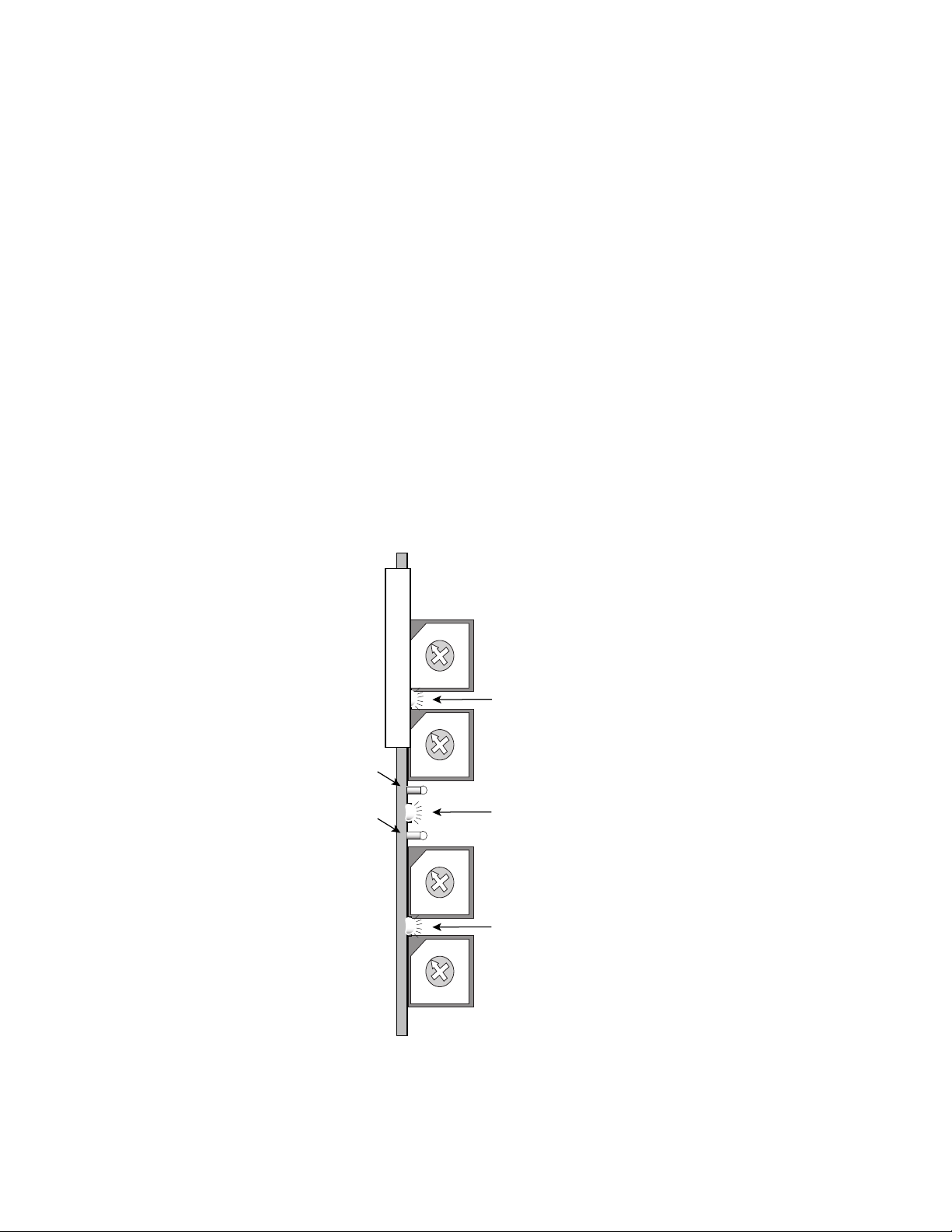
Adjustments, Testpoints, and Indicators
The 8914 DA has ground and +5V testpoints easily accessible on the front
edge of the module (see Figure 4).
Between the testpoints is a green Power On LED.
Each reclocking section is phase-locked to its AES input signal. The Lock
LEDs on the front of the module are on when the reclocking chip has locked
on the incoming AES data stream. There is one Lock LED for each channel
as shown.
unless it
5
6
4
7
3
8
2
9
Delay 1
A
Coarse increments
B
C
D
5
6
7
8
9
Delay 1
A
B
Fine increments
C
D
5
6
7
8
Delay 2
9
A
Coarse increments
B
C
D
5
6
7
8
Delay 2
9
A
Fine increments
B
C
D
Green LED indicates
Phase Lock Channel 1
Green LED indicates
Power On
Green LED indicates
Phase Lock Channel 2
+5V Testpoint
Ground Testpoint
0547_02
1
0
F
E
4
3
2
1
0
F
E
4
3
2
1
0
F
E
4
3
2
1
0
F
E
Figure 4. 8914 Adjustments, Testpoints, and Indicators
4 8914 Instruction Manual
Page 11

Delay Adjustments
Signal delay for each channel is set by two 16-position rotary switches that
provide additive coarse and fine adjustments. The amount of both the
inherent delay of the signal path and the increments of induced delay
varies according to signal data rate. Table 1 provides delay figures for the
three accepted AES data rates—48 KHz, 44.1 KHz, and 32 KHz.
Table 1. Delay Adjustment Settings
Adjustments, Testpoints, and Indicators
Input
Signal
48 KHz 1.2 ms
44.1 KHz 1.305 ms
32 KHz 1.799 ms
Minimum Delay
(switches @ 0,0)
48 KHz Input Signal Example
Inherent (minimum) circuit delay with no set delay adjustment (rotary
switches at 0, 0) is 1.2 ms. Any switch setting above 0,0 masks the inherent
delay and, starting at 2 ms, adds the selected number of delay increments.
For example, setting Coarse to 0 and Fine to 1 produces 2 ms of delay. Each
additional Fine switch increment adds 2 ms.
Setting Coarse to 1 and Fine to 0 produces 32 ms of delay. Each additional
Coarse switch increment adds 32 ms.
Adjustment
Fine 2 ms (96 frames)
Coarse 32 ms (8 blocks)
Fine 2.177 ms (96 frames)
Coarse 34.88 ms (8 blocks)
Fine 3 ms (96 frames)
Coarse 48 ms (8 blocks)
Adjustment
Increment
Incremental
Delay Range
2 ms to 510 ms
2.177 ms to 555.9 ms
3 ms to 765 ms
8914 Instruction Manual 5
Page 12

8914 Dual AES/EBU Delay Distribution Amplifier
Specifications
Table 2. 8914 Specifications
Parameter Value
Inputs
Number Two (1 loopthrough, 1 terminated)
Signal type AES/EBU digital audio, per AES3id:1995 and SMPTE 276M
Connector 75
Return loss > 25 dB, 0.1 to 6 MHz
Frame Rates 32, 44.1, or 48 KHz (Automatic selection)
Outputs
Number Seven (4 delay channel one, 3 delay channel two)
Signal type AES/EBU digital audio, per AES3id:1995 and SMPTE 276M
Connector 75
Return loss > 25 dB, 0.1 to 6 MHz
Intrinsic Jitter < 6 ns
Performance
Minimum Output Delay 1.2 ms
Maximum Output Delay 510 ms (127.5 AES/EBU blocks)
Environmental
Operating temperature range 0 to 45° C, noncondensing
Non-operating temperature range -10 to +70° C, noncondensing
Power Requirements
Supply Voltage +12 Volts
Power consumption 3.5 Watts
Physical
Frame Resides in standard 2 rack unit 8900 Series frame
Ω BNC
Ω BNC
6 8914 Instruction Manual
Page 13

Service
Service
The 8914 modules make extensive use of surface-mount technology and
programmed parts to achieve compact size and adherence to demanding
technical specifications. Circuit modules should not be serviced in the field.
If your module is not operating correctly, proceed as follows:
■
Check frame and module power and signal present LED.
■
Check for presence and quality of input signals.
■
Verify that source equipment is operating correctly.
■
Check cable connections.
■
Check output connections for correct I/O mapping (correct input is
used for the corresponding channel output).
Refer to Figure 4 for supply voltage test points on the 8914 module.
If the module is still not operating correctly, replace it with a known good
spare and return the faulty module to a designated Grass Valley repair
depot. Call your Grass Valley representative for depot location.
Refer to the
Contacting Grass Valley Group at the front of this document for
the Grass Valley Customer Service Information number.
8914 Instruction Manual 7
Page 14

8914 Dual AES/EBU Delay Distribution Amplifier
Functional Description
Refer to the block diagram in Figure 5 while reading the description.
There are 2 inputs for the module. One of these inputs is a loop-through
input. The data paths are otherwise conceptually identical for both inputs.
The inputs are first received by the receive circuit. Next, the Field Program-
mable Gate Array (FPGA) sends the data to the FIFO, which returns the
data to the FPGA. Finally, the data is passed to the transmit circuit.
Fine
Fine
Serial Data
Clock
Control
Serial Data
Clock
Control
Programmable
AES Input 1
Loop-through
AES Input 2
AES/EBU
Receiver
AES/EBU
Receiver
Delay Select Switches
Delay 1
Delay 2
Coarse
Coarse
Field
Gate Array
(FPGA)
Parallel Data
Control
Parallel Data
Parallel Data
Control
Parallel Data
AES Outputs
Delay
1
Line
Drivers
FIFO
FIFO
(Transmit)
Lock Ch. 1
Lock Ch. 2
Delay
2
0547-01
Figure 5. 8914 Dual AES/EBU Delay DA Block Diagram
Receive Circuit
This circuit features a digital audio transformer conforming to EBU stan-
dards.
The AES/EBU receiver recovers audio data and low jitter clocks from the
digital audio input transmission line. The data is reclocked, and then sent
to the FPGA. A special mode allows the preamble and bi-phase mark data
to pass through in its entirety. The 6.144 MHz clock signal is also sent to the
FPGA.
FPGA
The FPGA is a field programmable gate array containing proprietary Grass
Valley control circuitry. The FPGA converts the serial AES/EBU stream to
12-bit parallel data. The width of the data corresponds to the width of the
8 8914 Instruction Manual
Page 15

FIFO Circuits
Functional Description
FIFO (First In First Out) delay circuit. A small delay is introduced by the
nature of the serial to parallel circuit. The output goes to the external FIFO
chip.
The FIFO circuits are used to create various amounts signal delay. In the
FPGA, a separate controller is provided for each data stream to the FIFOs.
The two controllers perform the same functions. The controller outputs the
following signals: read reset, write reset, read clock, and write clock. The
read and write clocks are the same signal, and its frequency is determined
by the width of the parallel data.
The amount of delay is determined by two 16-position rotary switches.
Depending on input signal rate, the Fine switch delays the data by 2 to 3 ms
increments. The Coarse switch delays the data by 30 to 48 ms increments.
There is a minimum circuit delay of from 1.2 to 1.799 ms (for precise adjustment details, see
Adjustments, Testpoints, and Indicators on page 4 ).
The FIFO circuits create the signal delay. The FIFO receives parallel data
from the FPGA. All clock and control signals are provided by the FPGA.
The FIFO output is sent back to the FPGA.
Line Drivers
The delayed serial data is passed to the Line Driver (transmit) circuit.
Frequency Lock LEDs
The logic to turn on and off the Signal Lock LEDs is provided by the three
Error pins from the AES/EBU receiver. A no lock error condition (Lock
LED off) indicates that the phase-lock loop in the receiver is not locked to
the incoming data stream or the input signal is not present.
8914 Instruction Manual 9
Page 16

8914 Dual AES/EBU Delay Distribution Amplifier
10 8914 Instruction Manual
Page 17

Index
A
adjustments
1, 4
B
block diagram
8
C
cabling
circuit diagram
connections
controller module
input
output
3
8
3
3
3
D
delay adjustments
2
1, 4, 5
specification 6
L
LEDs 4
lock 4
M
module
controller
installation 2
power supply 2
2
O
outputs 6
connectors 4
specification 6
termination 3, 4
E
environmental specifications
F
frame
2, 3, 6
6
P
performance 6
phase lock 5
power requirements 6
power supply 2
R
G
repair depot 7
ground
I
impedance
indicator
input
8914 Instruction Manual Index-1
4
4
4
3, 6
loopthrough 3
rotary switch 1, 4
S
specifications 6
switch 4
delay 1
rotary 1
Page 18

T
termination 3
testpoints 4, 7
troubleshooting 7
Index-2 8914 Instruction Manual
 Loading...