

Page 1

Trademark:
Technical Manual
Of
Intel Haswell/Broadwell Series CPU
Based
3.5’’ SBC
SYS8F361VGGA
Revision: 2.0
Release date: June 23, 2015
* Specifications and Information contained in this documentation are furnished for information use only, and are
subject to change at any time without notice, and should not be construed as a commitment by manufacturer.
Page 2
Environmental Protection Announcement
Do not dispose this electronic device into the trash while discarding. To minimize
pollution and ensure environment protection of mother earth, please recycle.
ii
Page 3

TABLE OF CONTENT
ENVIRONMENTAL SAFETY INSTRUCTION...................................................................................iv
USER’S NOTICE
MANUAL REVISION INFORMATION................................................................................................ v
ITEM CHECKLIST..................................................................................................................................v
CHAPTER 1 INTRODUCTION OF THE MOTHERBOARD
1-1 FEATURE OF MOTHERBOARD.........................................................................................1
1-2 SPECIFICATION.................................................................................................................... 2
1-3 LAYOUT DIAGRAM
CHAPTER 2 HARDWARE INSTALLATION
2-1 JUMPER SETTING................................................................................................................ 11
2-2 CONNECTORS AND HEADERS
2-2-1 CONNECTORS........................................................................................................16
2-2-2 HEADERS................................................................................................................ 20
....................................................................................................................................
...............................................................................................................
........................................................................................
v
4
16
iii
Page 4

Chapter 1
Onboard
Intel
Haswell/Broadwell
series
SoC
Processor,
with
low
power
Introduction of the Motherboard
1-1 Feature of Motherboard
n
consumption never denies high performance
n Support 2 * DDR3L 1333/1600 MHz SO-DIMM, up to 16GB
n Support 1 * SATAIII device
n Onboard 1* full-size mSATA/ Mini-PCIE slot
n Onboard 1* half-size Mini-PCIE slot
n Onboard 2 * RJ-45 gigabit Ethernet LAN port
n Integrated with 1 * 24-bit dual channel LVDS header
n Support 2* HDMI output
n Support USB 3.0 data transport demand
n Support CPU Smart FAN
n Compliance with ErP standard
®
n Support Watchdog function
1
Page 5
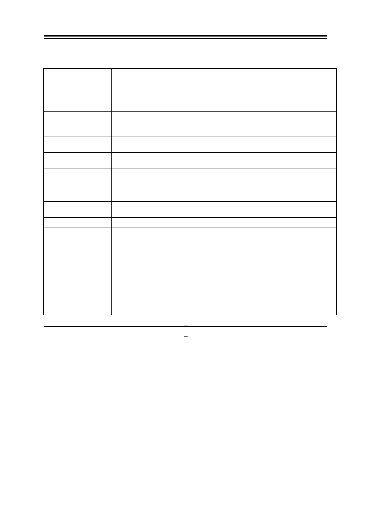
1-2 Specification
Spec
Description
Design
3.5”SBC
;
PCB
size:
14.8x
10.2
cm
Intel
Haswell/Boardwell
ULT
SoC
CPU
more
information
of
onboard
CPU.
Dual-channel
function
supported
1*
Full-size
Mini-PCIE/mSATA
slot
(MMPE)
1*
Half-size
Mini-PCIE
slot
(MPE)
Support
Fast
Ethernet
LAN
function
of
providing
10/100/1000Mb
ps
AMI
128MBFlash
ROM
4*
USB
3.0portl2*
RJ-45
LAN
portl2*
HDMI
port
l
l
Embedded CPU
Memory Slot
Expansion Slot
Storage
LAN Chip
Audio Chip
BIOS
*CPU model varies from different IPC options. Please consult your dealer for
2 * DDRIIIL SODIMM Slot for un-buffered DDRIIIL 1333/1600 MHz
l
SDRAM, expandable to 16GB
l
l
l
1* SATAIII 6G/s Connector (SATA1)
l
*SATA1 port & M-SATA connector (MMPE) supports RAID0/1 function.
Integrated with Intel I211AT PCI-E Gigabit PCI-E LAN chip & Intel
l
I218LM Gigabit LAN PHY chip
l
Ethernet data transfer rate
Realtek ALC662 HD Audio Codec integrated
l
Audio driver and utility included
l
l
Rear Panel I/O:
®
Multi I/O
1* DC 9V~24V power-in connector
l
2* USB 2.0 port
l
l
l
1* Audio Line out/Optical SPDIF out port
Internal I/O Connectors& Headers:
1* 2-pin 9V~24V DC-in internal power connector
l
2
Page 6
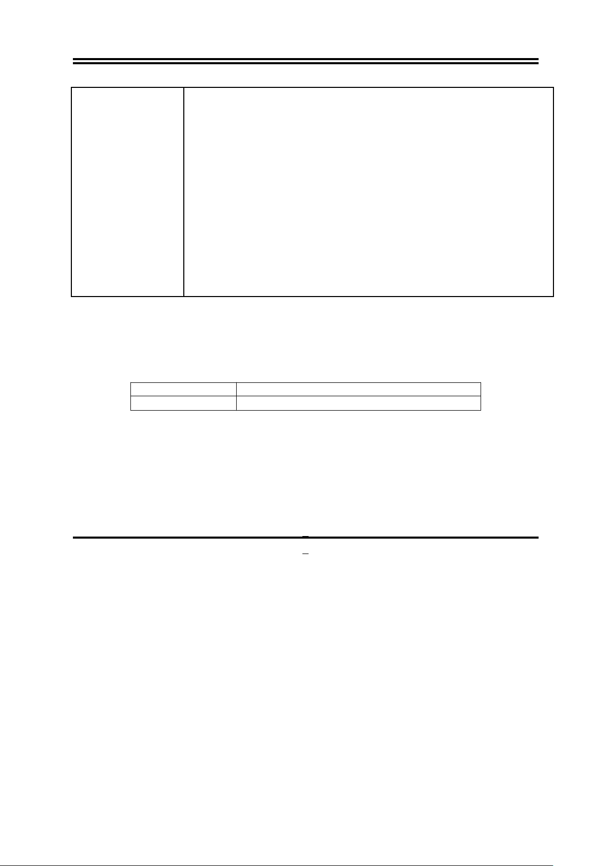
l
1*
SATAII
I6Gb/s
port
1*
Front
panel
audio
header
4*
Serial
port
header
(COM1
supports
RS422/RS485
function)
1*
9-pin
USB
2.0
header
(Expansible
to2*USB
2.0
ports)
1*
GPIO
header
1*
PS2KBMS
header
l
1*
Front
panel
header
JP8:
1*
LAN
LED
activity
header
1*
LVDS
inverter
Model
Power
Connector
1-3
Layout
Diagram
1* SATA Power connector
l
1* CPU FAN connector
l
l
1* SPK_OUT header (for 3W / 8 OHM amplifier)
l
l
l
1* 4-pin USB 2.0 header (Expansible to 1* USB 2.0 ports)
l
l
1* SMBUS header
l
l
l
l
1* LVDS header
l
Note: This manual serves as a common manual for SYS8F361VGGAseries. except
that power connector adopts 2-pin internal power connector, not DC-IN power jack on
the back panel.
Their main differences are listed as below:
SYS8F361VGGA
9V~24V DC Power-in Connector (On the rear I/O)
Note: The pictures for illustration examples in this manual are mostly taken from the
layout diagram for SYS8F361VGGA series, unless otherwise stated. Please refer
to your actual product for specification reference.
3
Page 7
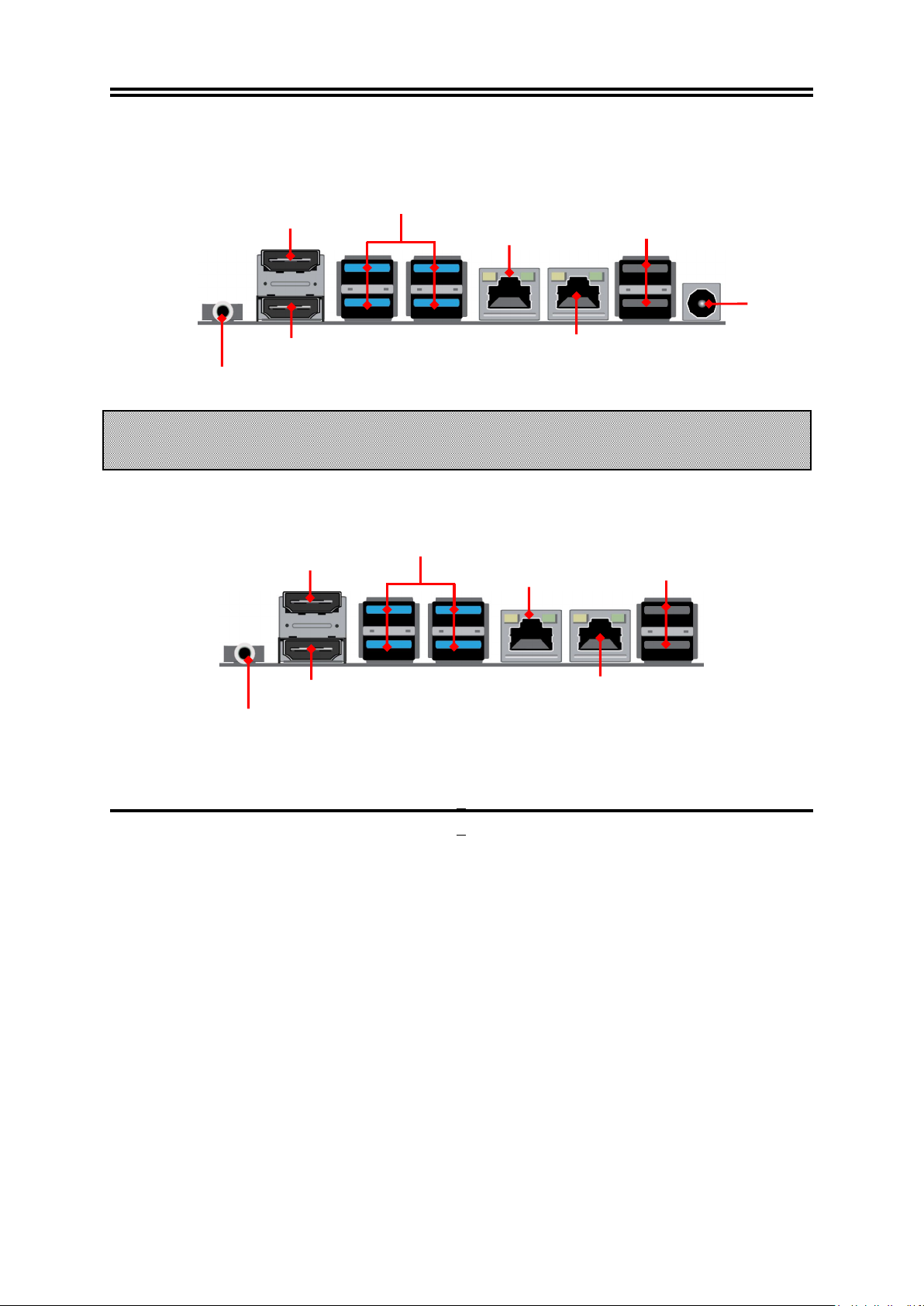
Rear IO Panel Diagram
connector
should
notbelower
than9Vor
higher
than
24V,
otherwise
it
maydoharm
to
the
board
&
other
devices!
USB
3.0
Ports
RJ-45
LAN
Port
RJ-45
LAN
Port
USB
2.0
Ports
USB
3.0
Ports
RJ-45
LAN
Port
RJ-45
LAN
Port
USB
2.0
Ports
For Power connector 2 Series Series:
HDMI1 Port
HDMI2 Port
Line-Out Port/
Optical SPDIF Out Port
*Notice: Please connect compatible power supply to the power connector. The voltage of power
LAN1
*9V~24V DC
Power-in
Connector
LAN2
For Power-in Connector 1 Series:
HDMI1 Port
LAN1
HDMI2 Port
Line-Out Port/
Optical SPDIF Out Port
Internal Diagram-Front Side:
LAN2
4
Page 8
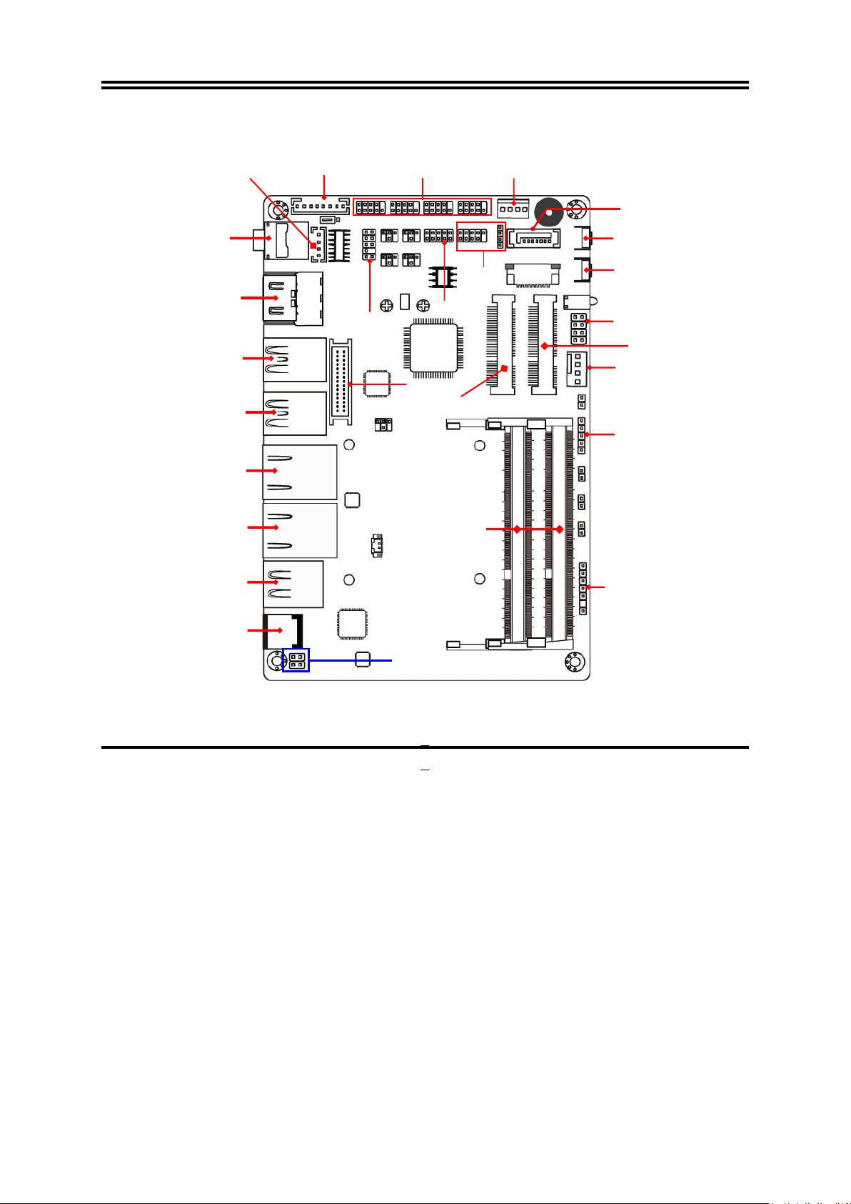
For Power Connector 1 Series:
JP8:
LANLED
Headers
CPUFAN
Header
Front
Panel
Header
DDR3L
SODIMM
Slots
Reset
Button
Power
Switch
Button
SMBUS
Header
INVERTER
LVDS
Header
USB
2.0
Headers
PS2KBMS
Header
USB
3.0
Ports
USB
3.0
Ports
USB
2.0
Ports
Mini-PCIE/mSATA
Slot
SPK_OUT
Header
Line-Out Port/
Optical SPDIF-Out Port
Serial Port Header
(COM4/3/2/1)
SATA Power
Connector
SATAIII Port
HDMI Ports
LAN1
RJ-45 LAN Port
LAN2
RJ-45 LAN Port
9V ~24V DC
Power-in Connector
Front Panel
Audio Header
GPIO Header
MPE:Half-size
Mini-PCIE Slot
MMPE: Full-size
5
Page 9
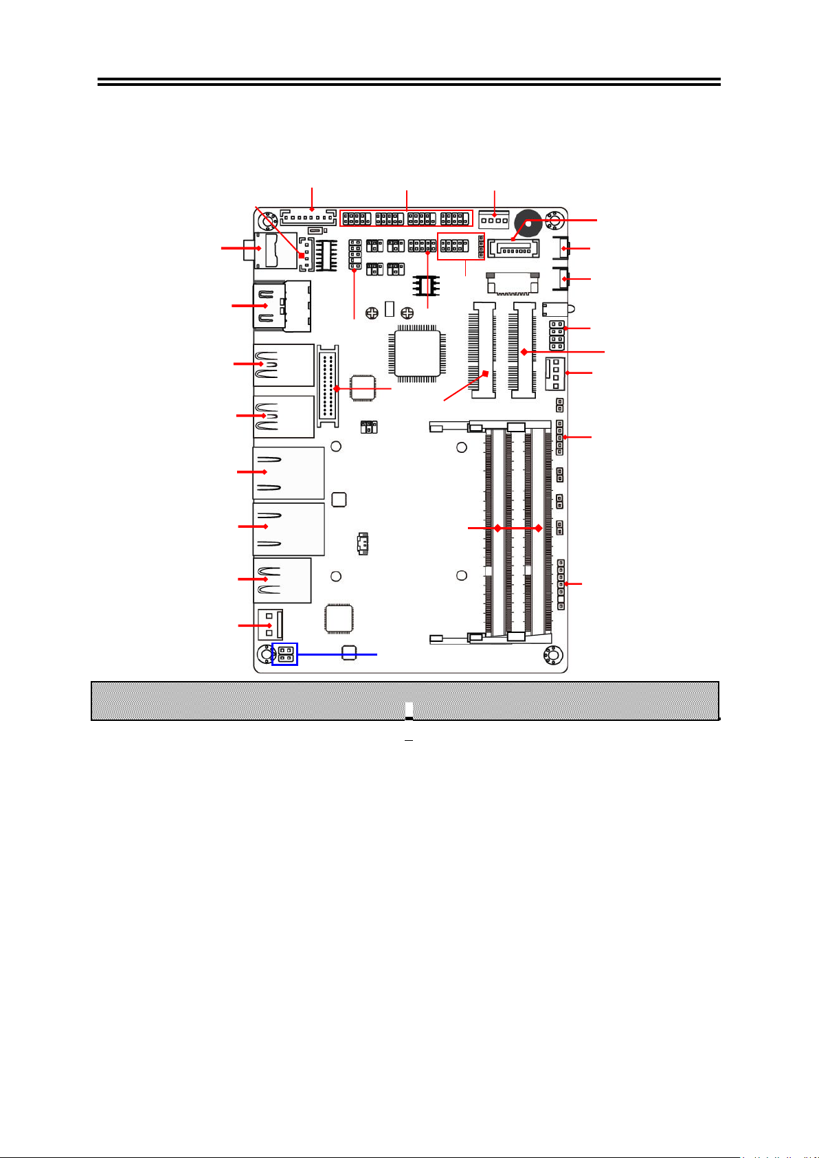
Internal Diagram-Front Side:
there
isnointerference
between
the
cards
installed.
JP8:
LANLED
Headers
CPUFAN
Header
Front
Panel
Header
DDR3L
SODIMM
Slots
Reset
Button
Power
Switch
Button
SMBUS
Header
INVERTER
USB
2.0
Headers
PS2KBMS
Header
USB
3.0
Ports
USB
3.0
Ports
USB
2.0
Ports
Mini-PCIE/mSATA
Slot
For Power connector 2 Series:
SPK_OUT
Header
Line-Out Port/
Optical SPDIF-Out Port
Serial Port Header
(COM4/3/2/1)
SATA Power
Connector
SATAIII Port
HDMI Ports
Front Panel
Audio Header
GPIO Header
LVDS Header
MPE:Half-size
Mini-PCIE Slot
MMPE: Full-size
LAN1
RJ-45 LAN Port
LAN2
RJ-45 LAN Port
Internal
9V ~24V DC-in
Power Connector
*Note: In the case that user wish to install two different cards to MPE & MMPE slot, make sure that
6
Page 10
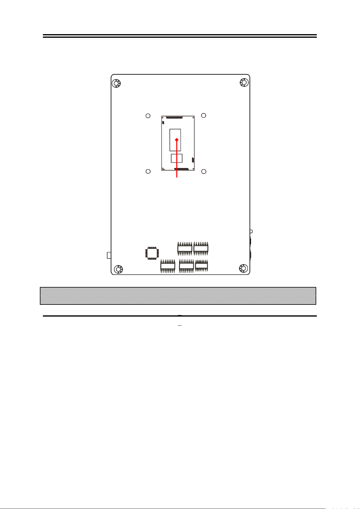
Internal Diagram-Back Side:
that
there
isnodamage
to
the
CPU
during
any
installation
procedures
!
*Intel CPU
*
Note: CPU is the most important part of the board and very fragile to any possible harm. Make sure
7
Page 11
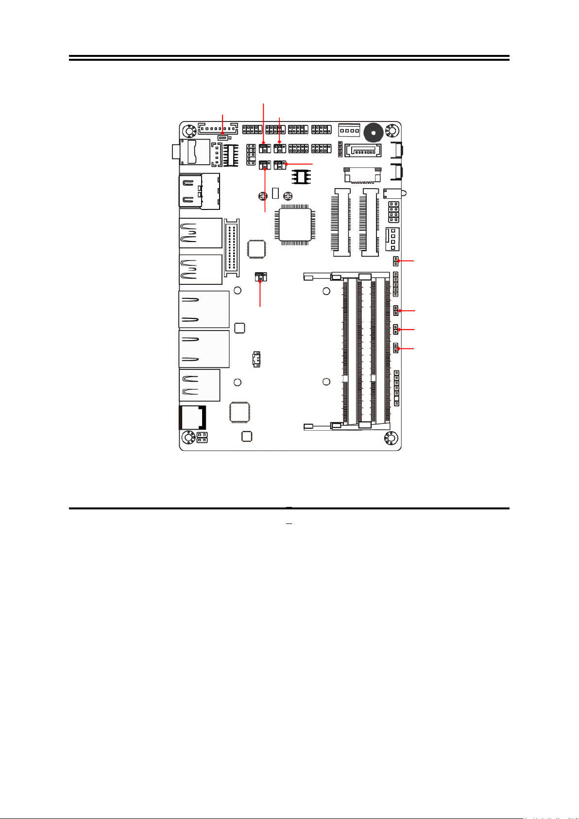
Jumper Position:
JP1
JP7
JP2
JP4
JP5
JP6
JP3
COPEN
AT-MODE
8
Page 12
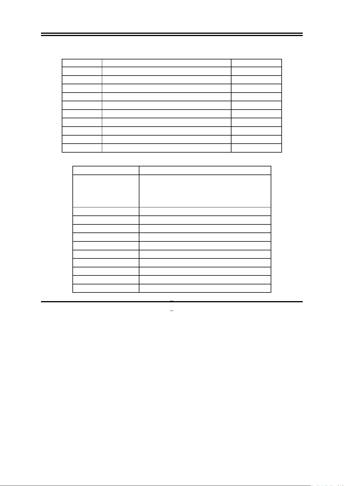
Jumper
Jumper
Name
Description
JP7COM
4
Header
Pin9
F
unction
Select
4-PinBlock
JP4COM
1
Header
Pin9
F
unction
Select
4-PinBlock
AT_MODE
AT
Mode
Function
Select
2
-Pin
Block
Internal
2-Pin
9V~24V
DC-in
Power
Connector
SATA1
SATAI
II
Port
Connector
PW
OUT
SATA
Power
out
Connector
U
SB1/USB3
USB
3.0
Port
Connector
X4USB5
USB
2.0
Port
Connector
s
X2
HDMI
DVI-I
Port
Connector
X2
LOUT
Audio
Line
Out
Connector
JP3 LVDS PVCC 5V/3.3V /12V Select 4-Pin Block
JP2 INVERTER VCC 5V/12V Select 3-Pin Block
JP5 COM3 Header Pin9 Function Select 4-Pin Block
JP6 COM2 Header Pin9 Function Select 4-Pin Block
JBAT CMOS RAM Clear Function Setting 2-Pin Block
COPEN Case Open Message Display Function 2-Pin Block
JP1 Security Measure Function Select 2-Pin Block
Connectors
*DCIN1 Power connector 1 Series: 9V~24V
Connector Name
DC-in Power Jack Connector
Power connector 2 Series:
CPUFAN CPUFAN Connector
LAN1/LAN2 RJ-45 LAN Port Connector X2
MMPE Full-size Mini-PCIE/MSATA Connector
MPE Half-size Mini-PCIE Connector
9
Page 13
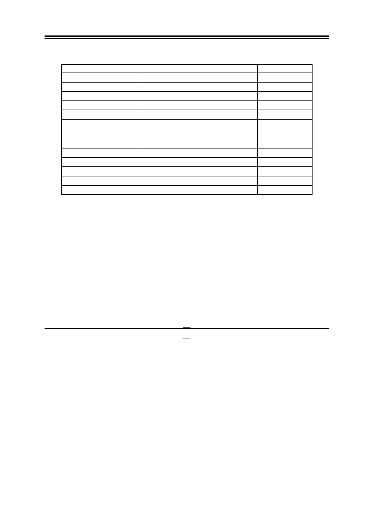
Headers
Header
Name
Description
COM
4/3/2/1
Serial
P
ort
Header
X4
9-pin
Block
GPIO
GPIO
Header
10-pin
Block
SMBUS
SMBUS
Header
5
-pin
Block
JP8
LAN
Activity
LED
Header
4-
pin
Block
LVDS
24-bit
LVDS
Header
30-pin
Block
FP_AUDIO Front Panel Audio Header 9-pin Block
SPK_CON Speaker Header 4-pin Block
USB4 USB 2.0 Header 9-pin Block
USB6 USB 2.0 Header 4-pin Block
FP Front Panel Header(PWR LED/
PS2KBMS PS2KBMS Header 6-pin Block
INVERTER LVDS Inverter Connector 8-pin Block
8-pin Block
HDD LED/Power Button /Reset)
10
Page 14
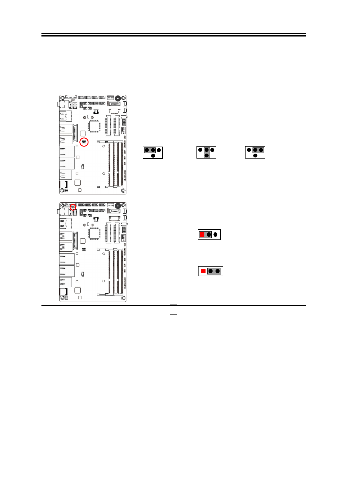
Chapter 2
LVDS VCC= 12V.
1 5 1 3 5 2 4 6 1 3 5 2 4 6
1
Hardware Installation
2-1 Jumper Setting
JP3 (4-pin): LVDS PVCC 3.3V/5V/12V Function Select
JP3→LVDS
6 4 2
3
2-4 Closed: LVDS
VCC= 3.3V;
JP2 (3-pin): INVERTER VCC 5V/12V Select
3-4 Closed: LVDS
VCC= 5V;
JP2→INVERTER
1 3
4-6 Closed:
1-2 Closed: Inverter VCC= 5V;
2-3 Closed: Inverter VCC= 12V.
11
Page 15
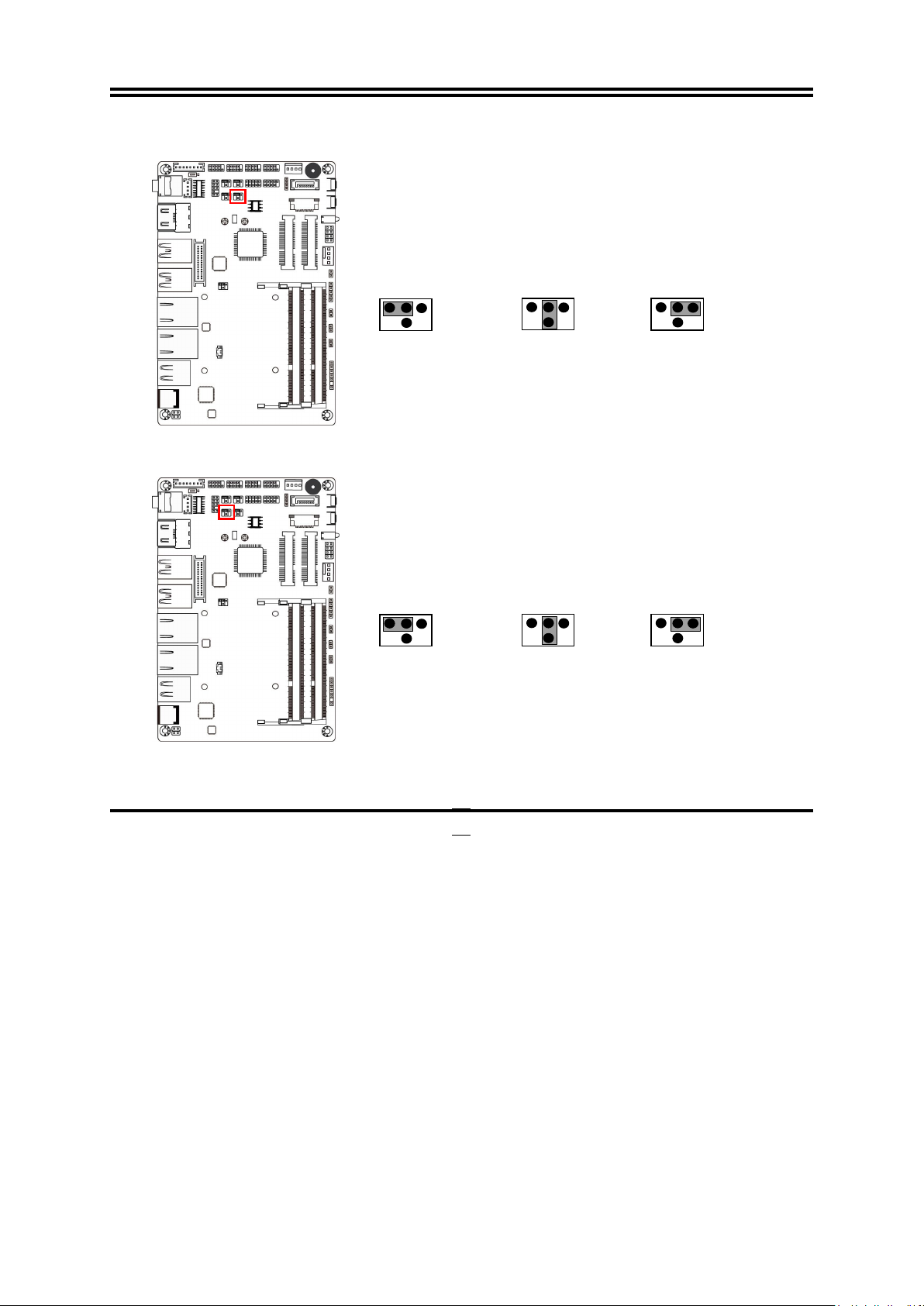
JP7 (4-pin): COM4 Header Pin9 Function Select
1 5 1 3 5 2 4 6 1 3 5 2 4 6
1 5 1 3 5 2 4 6 1 3 5 2 4 6
JP7→COM4
6 4 2
3
2-4 Closed:
RI=RS232;
3-4 Closed:
RI= 5V;
JP5 (4-pin): COM3 Header Pin9 Function Select
JP5→COM3
4-6 Closed:
RI= 12V.
6 4 2
3
2-4 Closed:
RI=RS232;
12
3-4 Closed:
RI= 5V;
4-6 Closed:
RI= 12V.
Page 16
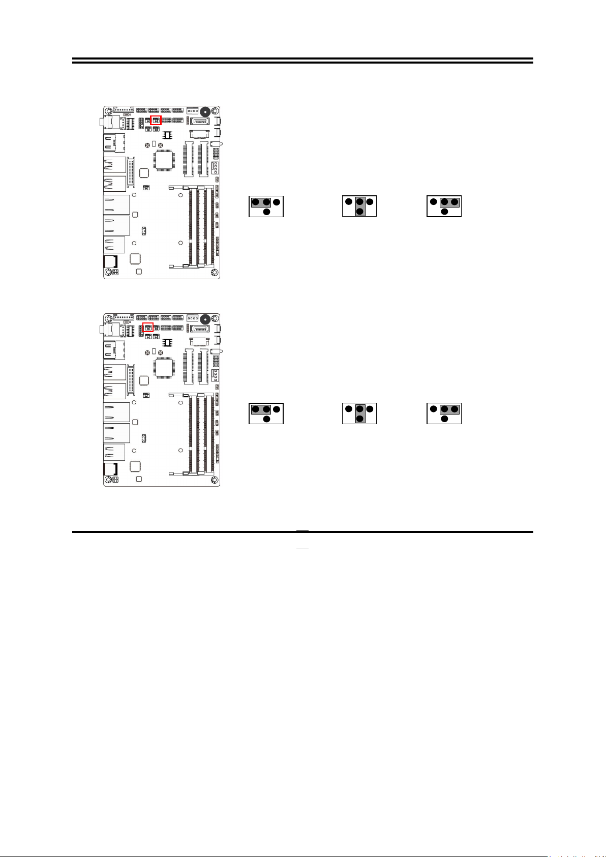
JP6 (4-pin): COM2 Header Pin9 Function Select
1 5 1 3 5 2 4 6 1 3 5 2 4 6
1 5 1 3 5 2 4 6 1 3 5 2 4 6
JP6→COM2
6 4 2
3
2-4 Closed:
RI=RS232;
3-4 Closed:
RI= 5V;
JP4 (4-pin): COM1 Header Pin9 Function Select
JP4→COM1
4-6 Closed:
RI= 12V.
6 4 2
3
2-4 Closed:
RI=RS232;
13
3-4 Closed:
RI= 5V;
4-6 Closed:
RI= 12V.
Page 17
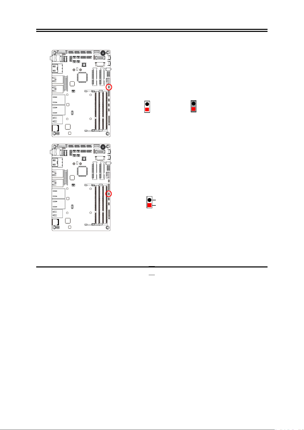
JBAT (2-pin): Clear CMOS
JBAT
1
1-2 Open: Normal;
1-2 Closed: Clear CMOS
CMOS Clear Setting
COPEN (2-pin): Case Open Message Display Function Select
COPEN
GND
1
Case open function
Pin 1-2 Closed: When Case open function pin short to GND, the Case open function
was detected. When Used, needs to enter BIOS and enable ‘Case Open Detect’
function. In this case if your case is removed, next time when you restart your
computer, a message will be displayed on screen to inform you of this.
14
Page 18
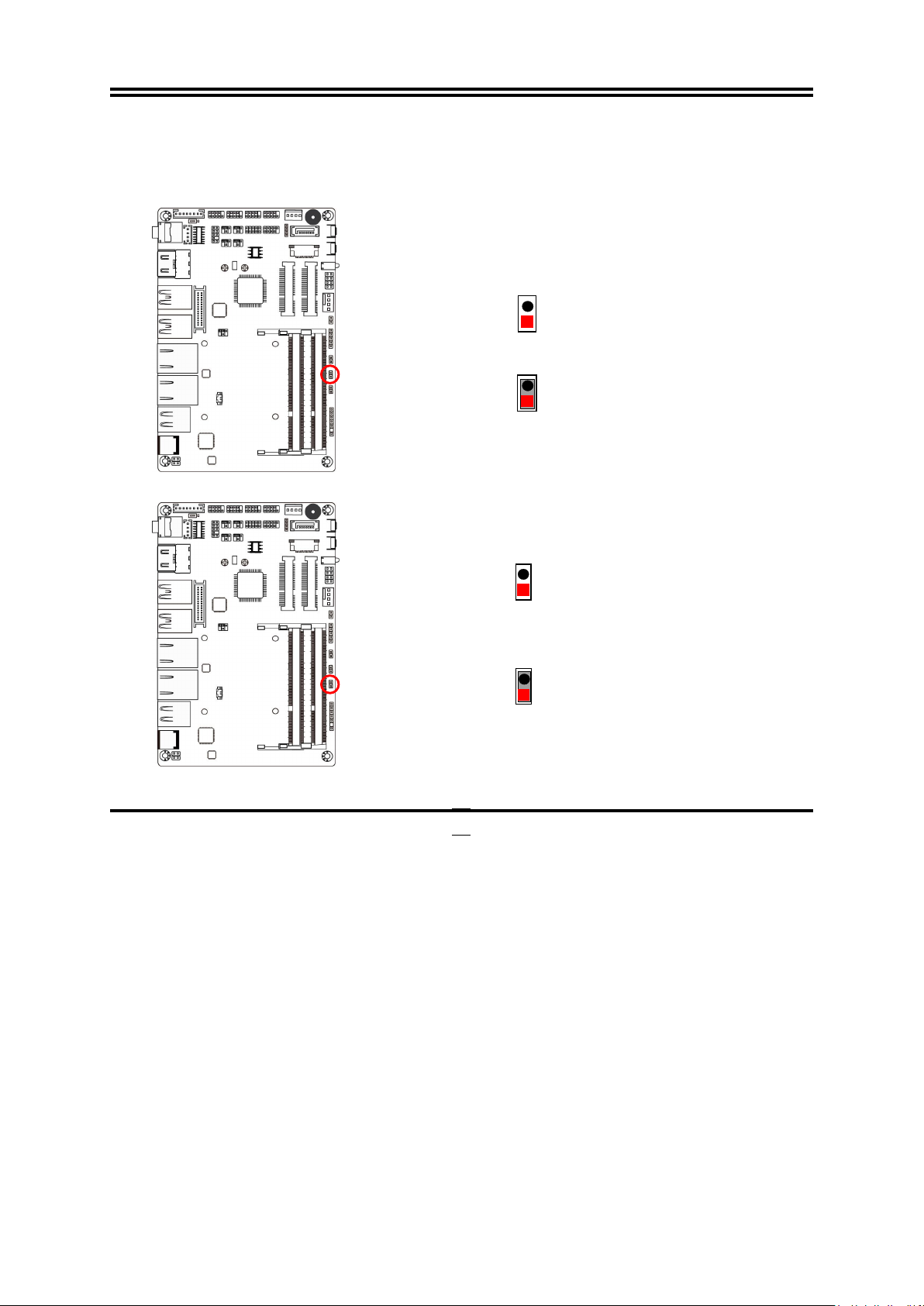
AT_MODE (2-pin): AT Mode Function Select
2
2
Pin 1-2 closed: AT_MODE function is enabled. In this case your computer will
automatically turns on after a sudden power failure when power supply resumes.
AT-MODE
1
1-2 Open: Normal;
1
1-2 Closed: AT Mode Selected.
JP1 (2-pin): Security Measure Function Select
JP7
1
1-2 Open:Enable Security Measures
in the Flash Descriptor(Default);
1
1-2 Closed: Disable Security Measures
in the Flash Descriptor(Override).
15
Page 19
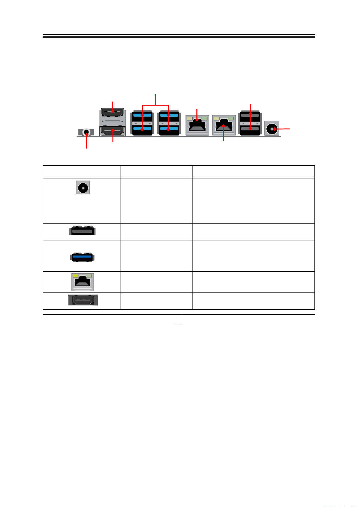
2-2 Connectors and Headers
(1)
Rear
I/O
Connectors
USB
3.0
Ports
RJ-45
LAN
Port
RJ-45
LAN
Port
USB
2.0
Ports
2-2-1 Connectors
HDMI1 Port
HDMI2 Port
Line-Out Port/
Optical SPDIF Out Port
Icon Name Function
(*Optional for Power
connector 2 Series
Series)
DC 9V~24V Power-in
Connector
USB 2.0 Port
USB 3.0 Port
RJ-45 LAN Port
LAN1
*9V~24V DC
Power-in
Connector
LAN2
For user to connect compatible power
adapter to provide power supply for the
system.
To connect USB keyboard, mouse or other
devices compatible with USB specification.
To connect USB keyboard, mouse or other
devices compatible with USB specification.
USB 3.0 ports supports up to 5Gbps data
transfer rate.
This connector is standard RJ-45 LAN jack
for Network connection.
(*Optional)
HDMI Port
To connect display device that support HDMI
specification.
16
Page 20
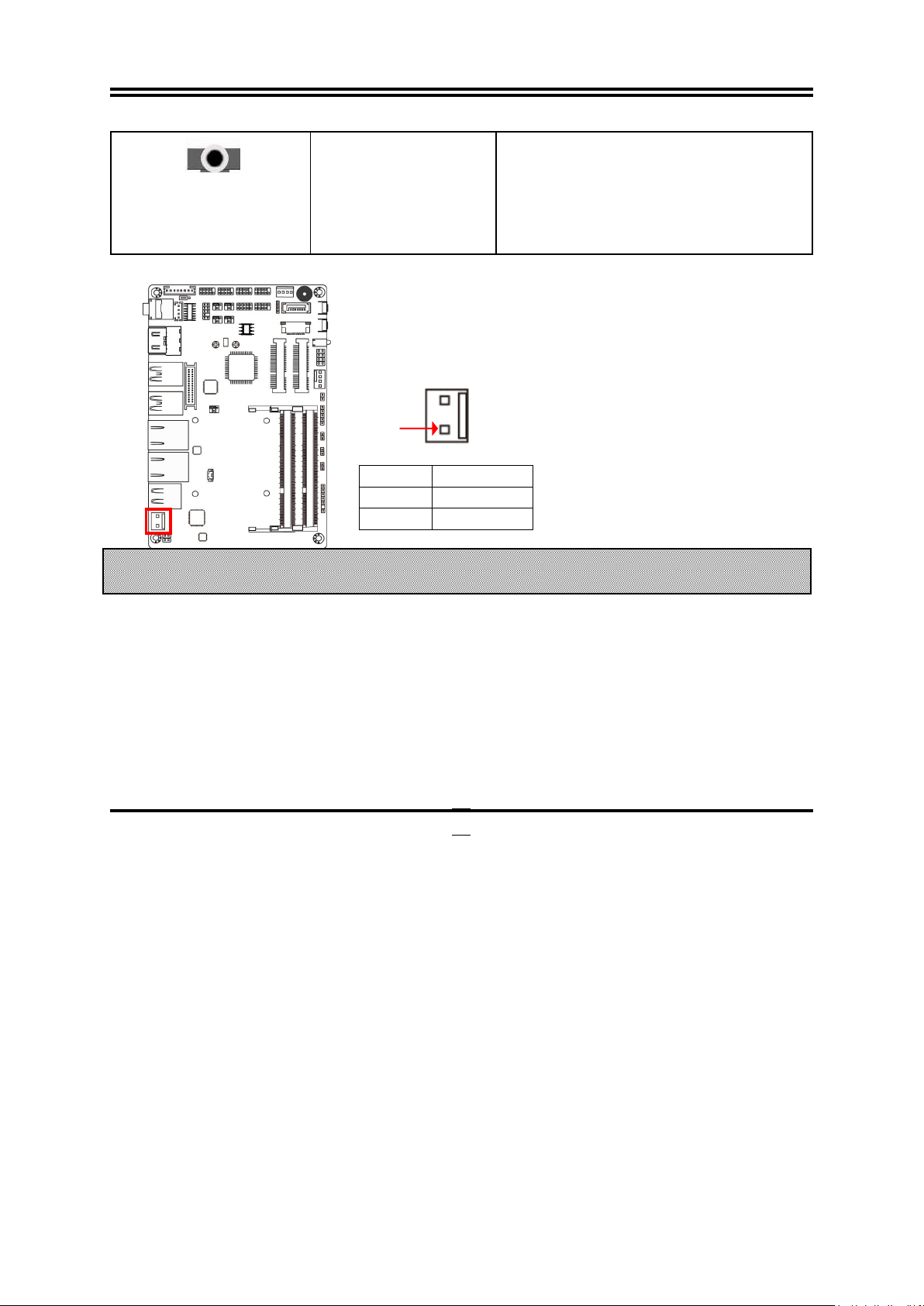
Line-Out Connector
(2)
DCIN1(2-pin)
:
9V~24V
DC-
in
Internal
Power
C
onnector
Pin1
INSTALLATION
DIRECTION
WILL
DAMAGE
THE
BOARD!!
/Optical SPDIF-Out
Connector
Pin No. Definition
1 +9V~+24V
2 GND
Warning: Find Pin-1 position before connecting power cable to this 2-pin power connector. WRONG
For user to connect external speaker,
earphones, etc to transfer system audio
output.
This connector can function as optical
SPDIF-Out jack with compatible cables &
devices.
17
Page 21
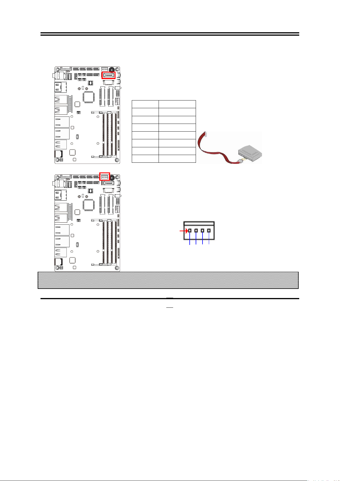
(3)
SATA1
(7-pin)
:
SATA
IIIPort
connector
SATA1 port is a high-speed SATAIII port that supports 6GB/s transfer rate.
(4)
PWROUT
(4-pin):
SATA
Hard
Disk
Power-out
Connector
Pin 1
+
12V
+
5
V
Pin-1
of
PWOUT
to
avoid
possible
damage
to
the
board
and
hard
disk
driver!
(5)
CPUFAN
(4-pin):
CPU
FAN
Connector
Pin No. Definition
1 GND
2 TXP
3 TXN
4 GND
5 RXN
6 RXP
7 GND
GND
Warning: Make sure that Pin-1 of compatible SATA Power connector is inserted into corresponding
GND
18
Page 22
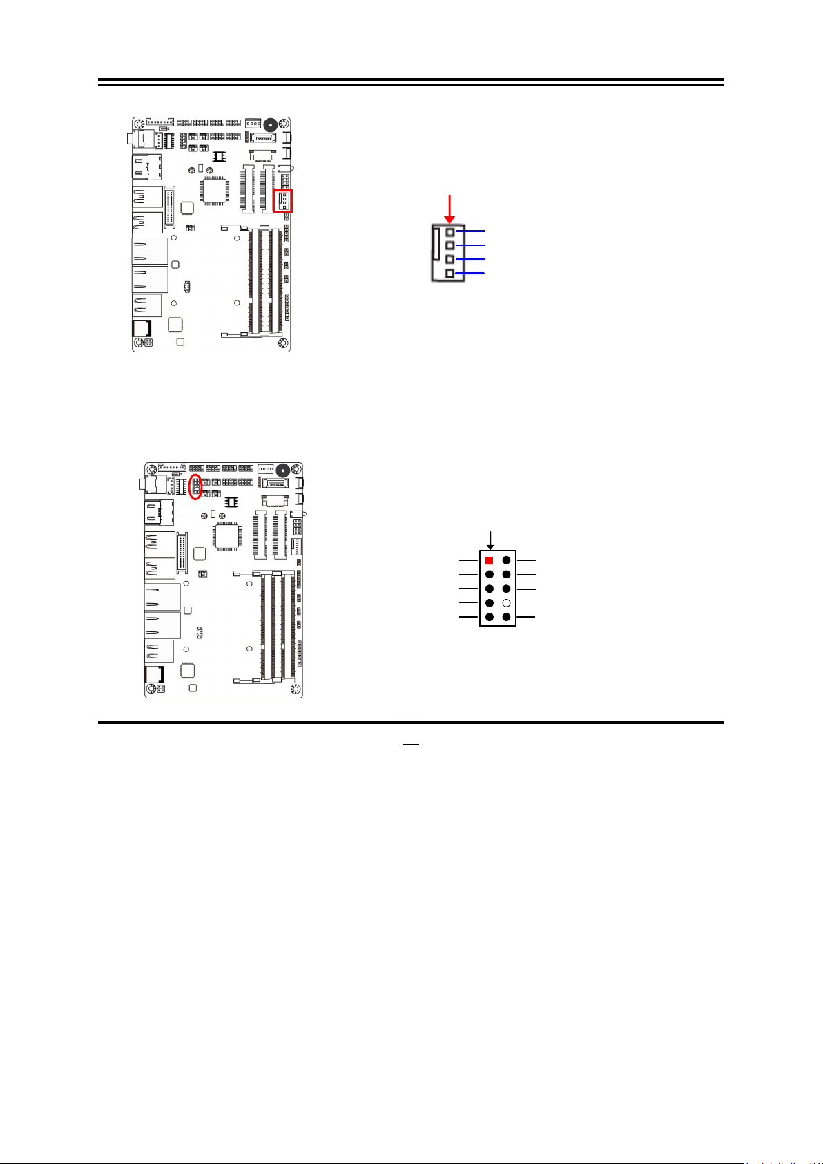
2
MIC-L
NC
Pin 1
GND
+12V Fan Power
Fan Speed
Control
2-2-2 Headers
(1) FP_AUDIO (9-pin): Line-Out, MIC-In Header
This header connects to Front Panel Line-out, MIC-In connector with cable.
Pin 1
GND
MIC-R
Lineout-R
NC
NC
Lineout-L
Line-Out, MIC Header
19
NC
Page 23
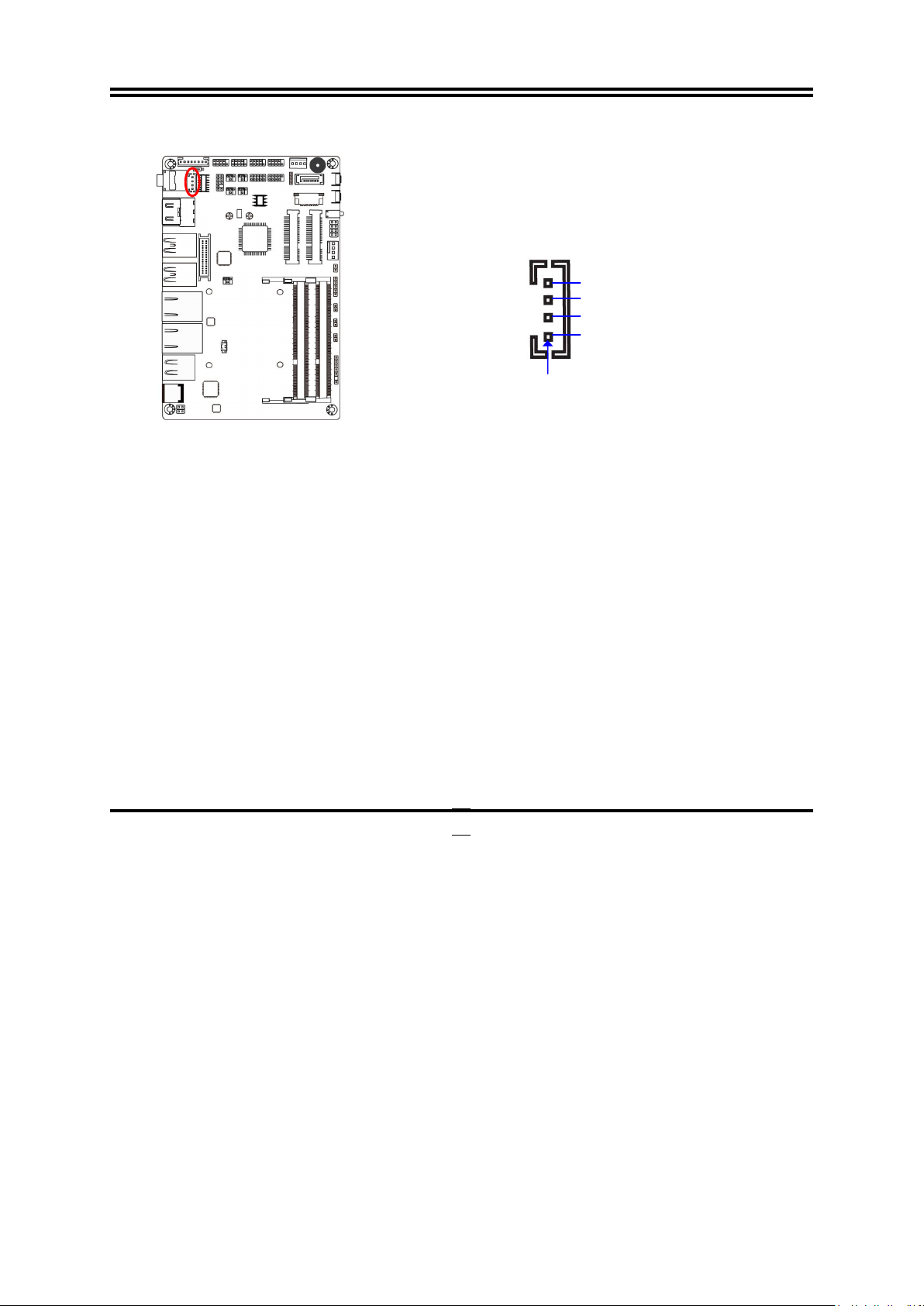
(2) SPK_OUT (4-pin): Speaker Header
1
L+ R+ R-
(3)COM4/3/2/1(9-Pin): Serial Port Headers
Pin
L-
20
Page 24
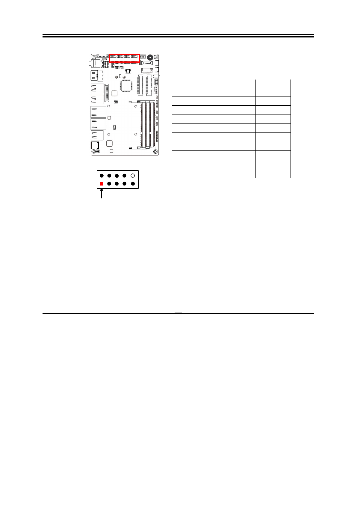
2
Pin 1
3
4
5
6
8
Pin NO. RS232 *RS422
(for COM1)
Pin 1
Pin 2 RXD
Pin 3 TXD
Pin 4
Pin 5
Pin 6
Pin 7
7
9
Pin 8
Pin 9
DCD TX- DATA-
TX+ DATA+
RX+ NC
DTR RX- NC
GND GND GND
DSR NC NC
RTS NC NC
CTS NC NC
RI NC NC
*RS485
(for COM1)
*Notice: RS422, RS485 function is supported by COM1 header only, with compatible
COM cable for RS422 or RS 485 function. User also needs to go to BIOS to set
‘Transmission Mode Select’ for COM1 (refer to Page 33).
(4) USB4 (9-pin): USB 2.0 Port Header
21
Page 25
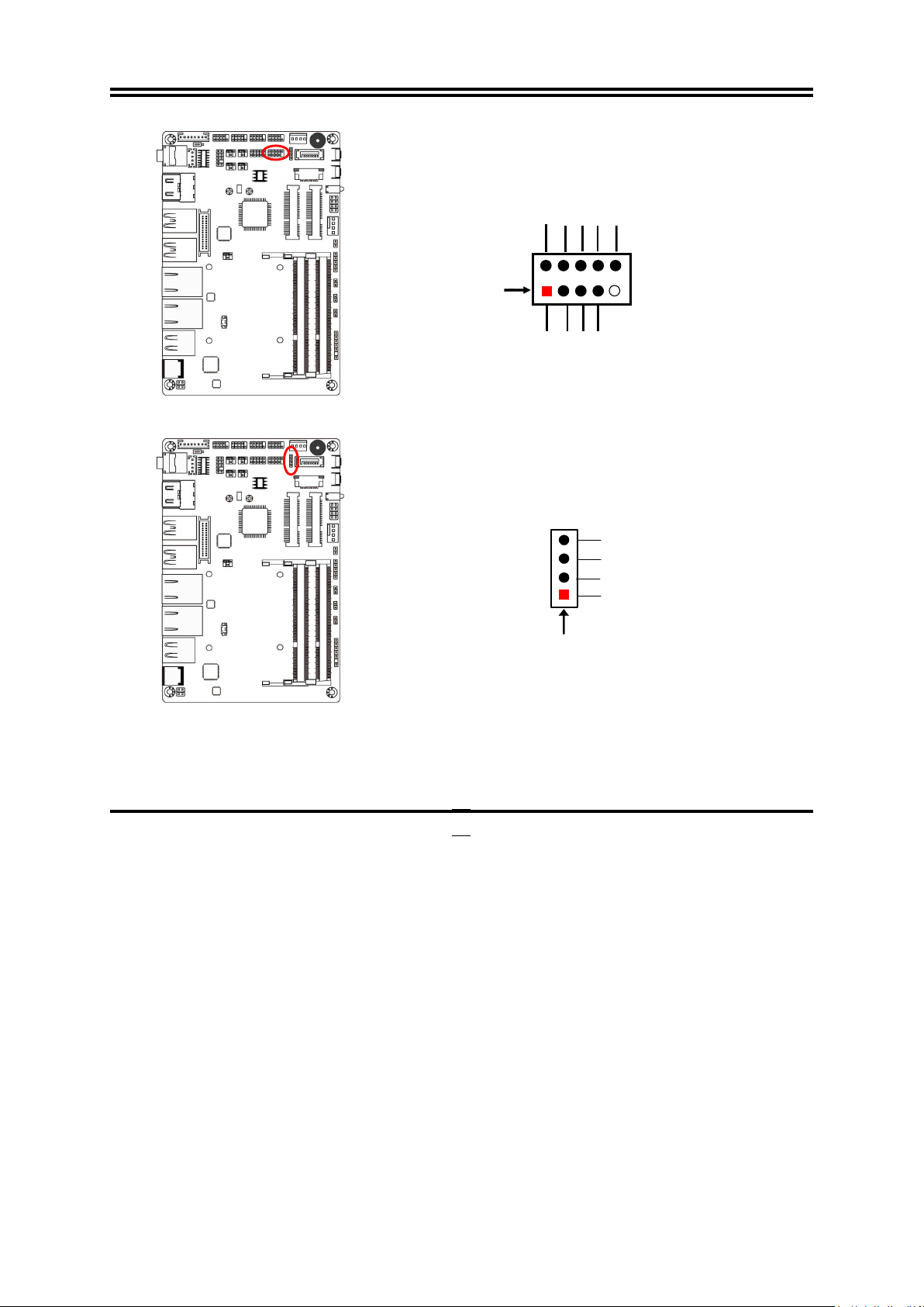
VCC
GND
GND
(5) USB6 (4-pin): USB 2.0 Port Header
Pin 1
+DATA
-DATA
NC
Pin 1
-DATA
+DATA
VCC
GND
+DATA
-DATA
VCC
(6) FP (8-pin): Front Panel Header
22
Page 26
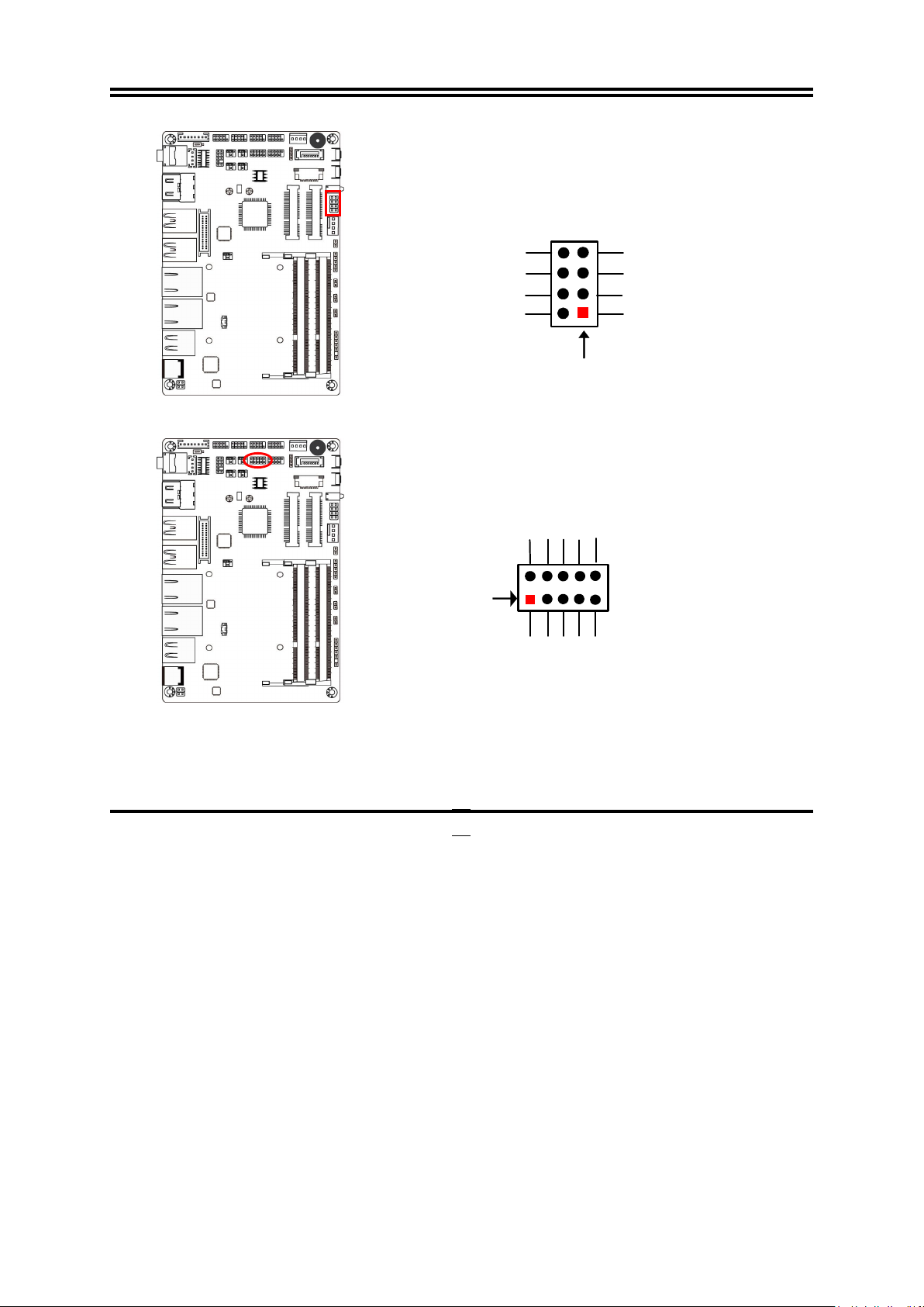
(7) GPIO (10-pin): GPIO Header
Pin 1
GND
PWRBTN
PWRLED -
PWRLED+
GND
RSTSW
HDDLED-
HDDLED+
2
Pin 1
(8) SMBUS (5-Pin): SM BUS Header
GPIO_83
GPIO_85 GPIO_87
GPIO_81
VCC
2
GPIO_84
GPIO_80
GPIO_82
GPIO_86
GND
23
Page 27
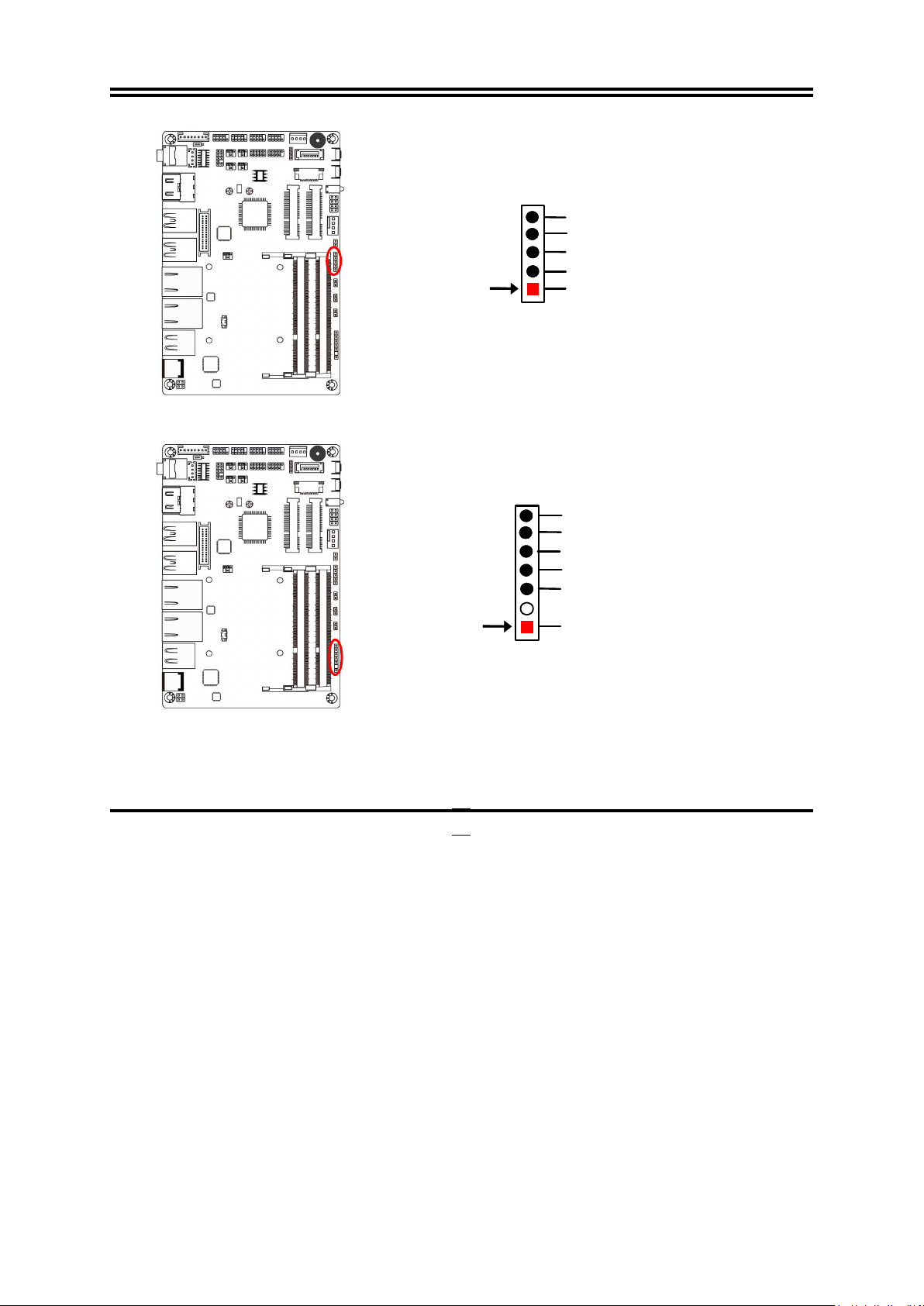
GND
VCC
3.3
SMBUS_ALERT-
GND
VCC
SMBUS_DATA
Pin 1
SMBUS_CLK
(9) PS2KBMS (6-pin): PS/2 Keyboard & Mouse Header
MS_DATA
MS_CLK
KB_CLK
KB_DATA
Pin 1
24
Page 28
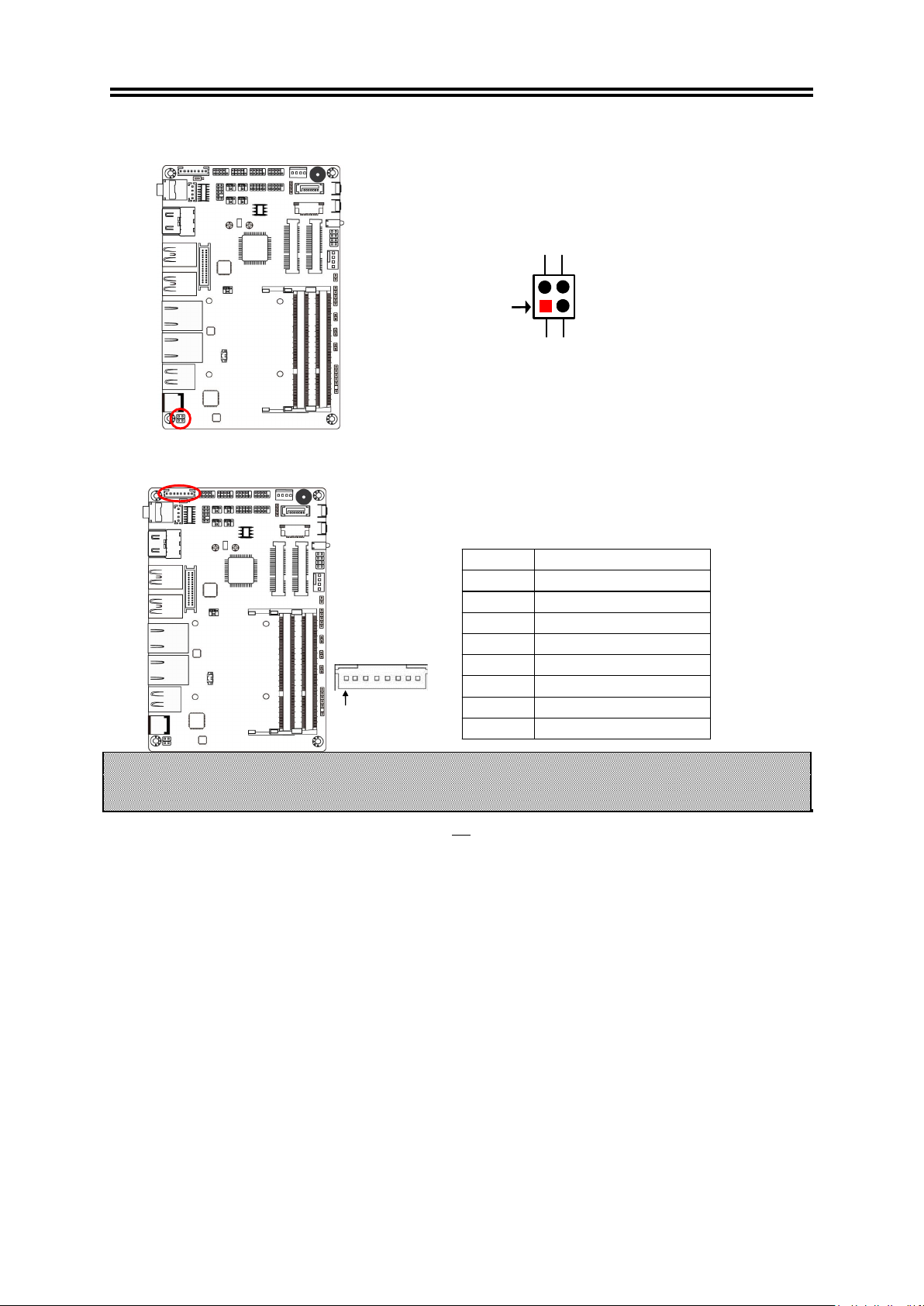
(10)JP8 (4-pin): LAN1 &LAN2 Activity LED Headers
Pin1
4 2
Otherwise
serious
harm
will
occur
to
the
board/display
panel!!
LAN1_LED- LAN2_LED-
LAN1_LED+
(11) INVERTER (8-pin): LVDS Inverter Connector
Pin No. Definition
1 Backlight Enable
Pin 1
2 Backlight PWM
3 PVCC
4 PVCC
5 GND
6 GND
7 Backlight Up SW
8 Backlight Down SW
3
LAN2_LED+
Warning! Find Pin-1 location of the inverter and make sure that the installation direction is correct!
25
Page 29
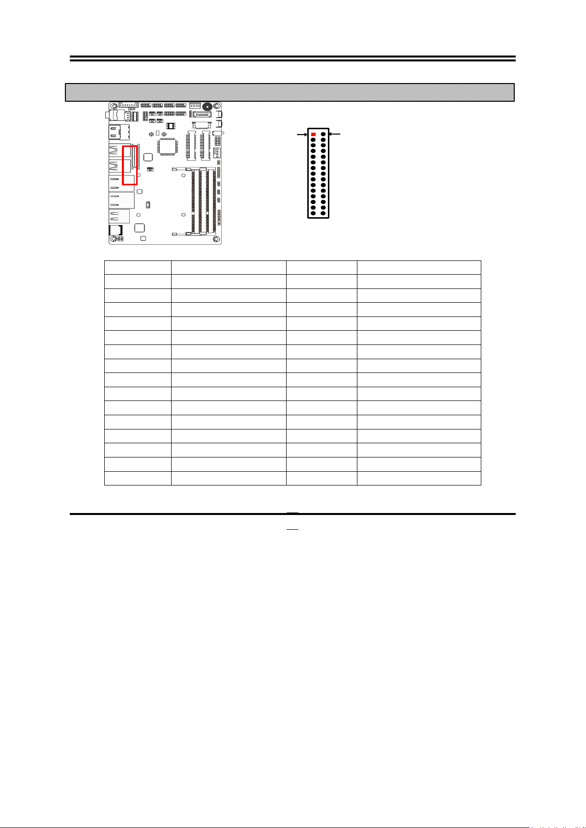
(12) LVDS (30-pin): 24-bit Dual Channel LVDS Header
Pin
NO.
Pin
Define
Pin
NO.
Pin
Define
Pin5LVDSB_DATAN2
Pin6LVDSB_DATAP2
Pin7LVDSB_DATAN1
Pin8LVDSB_DATAP1
Pin17LVDSA_DATAP3
Pin18LVDSA_DATAN3
Pin19LVDS_CLKAP
Pin20LVDS_CLKAN
Pin 1
Pin 2
Pin 1 LVDSB_DATAN3 Pin 2 LVDSB_DATAP3
Pin 3 LVDS_CLKBN Pin 4 LVDS_CLKBP
Pin 9 LVDSB_DATAN0 Pin 10 LVDSB_DATAP0
Pin 11 NC/DDC_DATA Pin 12 NC/DDC_CLK
Pin 13 GND Pin 14 GND
Pin 15 GND Pin 16 GND
Pin 21 LVDSA_DATAP2 Pin 22 LVDSA_DATAN2
Pin 23 LVDSA_DATAP1 Pin 24 LVDSA_DATAN1
Pin 25 LVDSA_DATAP0 Pin 26 LVDSA_DATAN0
Pin 27 PVCC Pin 28 PVCC
Pin 29 PVCC Pin 30 PVCC
26
 Loading...