

Grafenthal USV PTR-6000 Service Handbook

Service-Handbuch
GRAFENTHAL
USV PTR-6000
GRAFENTHAL GmbH • von-Monschaw-Straße 3 • 47574 Goch • info@grafenthal.de • www.grafenthal.de
Copyright © 2016 GRAFENTHAL GmbH, Alle Rechte vorbehalten. GRAFENTHAL ist eine eingetragene Marke der GRAFENTHAL GmbH.

2
CONTENT
1. GENERAL INFORMATION ....................................................................................................................................... 4
1.1 GETTING START ........................................................................................................................................................ 4
1.2 IMPORTANT SAFETY INSTRUCTIONS ........................................................................................................................ 4
2. ELECTRIC SPECIFICATIONS .................................................................................................................................. 5
3. FUNCTIONAL BLOCK ............................................................................................................................................... 7
4. WORKING PRINCIPLE OF THE MAJOR FUNCTIONAL BLOCK ..................................................................... 9
4.1 SWITCH POWER SUPPLY ......................................................................................................................................... 9
4.2 PFC/BOOSTER ........................................................................................................................................................ 9
4.3 INVERTER ................................................................................................................................................................. 9
4.4 CHARGER ............................................................................................................................................................... 10
4.5 EMI BOARD ............................................................................................................................................................ 10
5. FUNCTION EXPLANATIONS FOR EACH PCB .................................................................................................. 11
5.1 SPS-CHARGER BOARD (POWER STAGE BOARD) ................................................................................................. 11
5.2 CNTL BOARD (CONTROL BOARD) ......................................................................................................................... 11
5.3 COMMUNICATION BOARD ....................................................................................................................................... 11
5.4 EMI BOARD ............................................................................................................................................................ 11
5.5 MAIN POWER BOARD ................................ ................................................................................................ ............. 11
5.6 PARA(A) AND PARA(B) BOARD ............................................................................................................................... 11
5.7 O/P RELAY BOARD ................................................................................................................................................. 12
6. INTERFACE ............................................................................................................................................................... 13
6.1 LED DISPLAY ................................................................................................................................ ......................... 13
6.2 LCD DISPLAY ......................................................................................................................................................... 13
6.3 LCD DISPLAY ICON ................................................................................................................................................ 13
7. TROUBLE SHOOTING ............................................................................................................................................ 16
7.1 LCD PANEL DISPLAY PATTERN DEFINITION .......................................................................................................... 16
7.1.1 Trouble shooting for warning icon in LCD display ......................................................................................... 16
7.1.2 Trouble shooting for fault codes in LCD display ............................................................................................. 17
7.1.3 Trouble shooting .............................................................................................................................................. 18
7.2 REPAIR ................................................................................................................................................................... 18
7.2.1 Basic Instruments and tools ............................................................................................................................. 19
7.2.2 Configuration of the Model Port on the Control Board .................................................................................. 19
7.2.3 Configuration of the charger current on the charger Board ........................................................................... 19
7.2.4 Configuration of the
7.2.5 Regulation of the system .................................................................................................................................. 20
7.2.6 Quick Start ....................................................................................................................................................... 21
8. TEST STEP ................................................................................................................................................................ 23
charge voltage
on the charger Board ........................................................................... 19
9. APPENDIX ................................................................................................................................................................. 24
9.1 REFERENCE WAVEFORM ....................................................................................................................................... 24

3
9.2 BASIC COMMUNICATION COMMAND ........................................................................................................................ 26
9.2.1 QGS ................................................................................................................................................................. 26
9.2.2 V<n> ............................................................................................................................................................... 27
9.2.3 V±<n> ............................................................................................................................................................. 27
9.2.4 BUSP±<n> ...................................................................................................................................................... 27
9. 2.5 BUSN±<n> .................................................................................................................................................... 28
9. 2.6 VB±<n> ......................................................................................................................................................... 28
9.2.7 QVFW .............................................................................................................................................................. 28
9.2.8 OC±<n> .......................................................................................................................................................... 28
4
1. General Information
1.1 Getting start
This manual is for Galleon II 6K(L)/10K(L) tower UPS. It can help service person perform the basic
maintenance and repair service.
This manual only focuses on the service section, so you should get the basic operation of the UPS from
the user manual, and make sure you had read and understood the user manual before reading the
manual.
The manual include 9 sections:
● General Information, this section shows you the general information of the service manual.
● Electric Specifications, this section shows you the basic electric specification of the UPS.
● Functional block, this section shows you the major functional block of the UPS.
● Working Principle of the Major Functional Block, this section shows you the working principle of
the major functional block.
● Function explanations for each PCB, this section explains you all the PCBs of the UPS system.
● Interface, this section shows you the LCD interface, including display and setting.
● Trouble Shooting, this section gives you the way to find the problems.
● Test Step, this section tells you how to test the UPS after you repair the unit.
● Appendix, this section shows you the basic waveforms for reference and the basic communication
commands.
1.2 Important Safety Instructions
For qualified service person only.
DO NOT perform any internal service or adjustment of this product unless the technical person is
well trained and experienced. .
Dangerous voltage exists at several points in this product. To avoid personal injury, don't touch
any exposed connections or components while UPS is on.
Turn off the UPS and switch off the input breaker before removing protective case.
AC voltage is always present if the input AC power is still available.
High voltage may exist at DC capacitors. Before removing the protective case, wait for at least
five minutes after turning off the UPS.
Verify input source (voltage and frequency) is within the maximum range before service.

5
2. Electric Specifications
MODEL
SPECIFICATION
6K
6KL
10K
10KL
Input
Input Voltage
176~300 VAC @ Full Load
110 VAC @ Half Load
Input Frequency
46~54 Hz for 50Hz system
56~64 Hz for 60Hz system
Input Power Factor
≥0.99
Input THD
<4%
Generator
Support
Output
Output Power (VA/Watt)
6000/6000( 20 pieces battery)
10000/10000( 20 pieces battery)
6000/5400( 18~19 pieces battery)
10000/9000(18~19 pieces battery)
6000/4800(16~17 pieces battery)
10000/8000(16~17 pieces battery)
Nominal Output Voltage
208/220/230/240VAC
Voltage Regulation
±1%
Output Frequency
Follows Bypass Frequency in Line Mode
(50/60+0.1) Hz in Battery Mode
Voltage Distortion
≤6% @ Full Nonlinear Load
≤2% @ Full Linear Load
Current Crest Ratio
3:1
Transfer Time
0ms @ Line Battery
0ms @ Inverter Bypass
<10ms @ Inverter ECO
Short Circuit Protection
Yes
Battery
Nominal Battery Voltage
240 VDC
Nominal Battery Quantity
20 pcs
Acceptable Battery Quantity
18~20 pcs
Type/Capacity
12V/7.2Ah
12V/9Ah
Backup Time
≥6minutes@full load
≥4minutes@full load
Efficiency
To Line Mode
>93%
To Battery Mode
>91%
To ECO Mode
>96%
Overload Protection
100%~110%
Alarm and Transfer To Bypass after 10min @ Line mode
Alarm and Cut Off Output after 30s @ Battery mode
110%~130%
Alarm and Transfer To Bypass after 1min @ Line mode
Alarm and Cut Off Output after 10s @ Battery mode
Over 130%
Alarm and Transfer To Bypass after 1s @ Line mode
Alarm and Cut Off Output after 1s @ Battery mode

6
Alarm and Cut Off Output after 1min @ Bypass mode
Auto Retransfer
Yes
Interface
RS232
Yes
USB 1.1
Yes
EPO
Yes
Environment
OperatingTemperature
0 ℃ to 40℃
Humidity
<95% (No condensing)
Acoustic Noise
≤55dB
≤58dB
Standard
ESD
IEC 61000-4-2 Level 4
RS
IEC 61000-4-3 Level 3
EFT
IEC 61000-4-4 Level 4
Surge
IEC 61000-4-5 Level 4
Conduction
IEC/EN 62040-2 Category C3
Radiation
Safety
IEC62040-1-1
Drop
ASTM D5276-94
Vibration
ASTM D4728-87
Mechanical
Inlet
Terminal Block
Outlet
Terminal Block and Receptacle
7
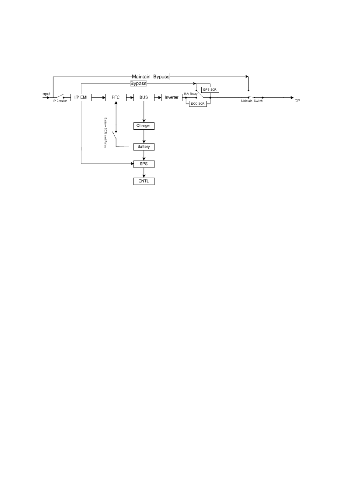
3. Functional Block
As a true online UPS, the product applies a double conversion topology, comprising functional blocks as
shown in Figure 3.1
Figure 3.1 Function block Diagram
The CNTL block controls the action of the UPS system. It also provides the communication interface for
receiving and executing command from users via the panel or other communication protocol. When the
UPS becomes abnormal, in most case, the CNTL can provide basic information indicating the status of
the UPS.
The Rectifier and PFC blocks are the input stage of the UPS. The blocks convert AC input power into
two stable DC power stored in the BUS capacitor. In the meantime, PFC (Power Factor Correction) will
be executed and allows input current tracking the input voltage waveform. Therefore, the input power
factor will be corrected to 1 to achieve maximum efficiency and produce lowest power pollution to the
utility.
The PFC block in battery mode, also called Booster, is used to convert the low voltage DC power to
higher voltage with stable DC power, stored in the BUS capacitor.
The Inverter block is the output stage of the UPS and used to convert DC power from the BUS capacitor
to sine waveform output power.
When the utility is within the acceptable range, the UPS will provide power directly from the utility input
and the Rectifier and PFC will be executed at the same time. When the utility is outside of the acceptable
range, no matter it’s because of input voltage or input frequency, the UPS will shut down the Rectifier
and PFC functions and turn on the Battery Booster. In case of sudden interruption from input utility, the
controller can detect the interruption in very short time. During the short interval of detecting the
interruption, the output power will be provided by the power stored in the BUS capacitor. In this way,
there is no any interruption on output power.
The charger charges the battery when the UPS system is in online model. You can set the current from
1A to 4A by changing the jumper. And you also can choose a different voltage corresponding to different
battery pieces by changing the jumper on the CNTL board and the charger board.
The Input EMI section provides EMI filter function. The input EMI filters can prevent the UPS from being
interference by external electronic/magnetic noise which is generated by other electronic system and

8
prevent other systems from the noise generated inside the UPS system.
The SPS generates DC power supply needed by operation of the circuit of the UPS itself. The Bypass
provides a path that utility can power the output directly when the Inverter is not executed. The
Maintenance Bypass provides another path that utility can power the output directly when UPS is in
maintenance status.
9
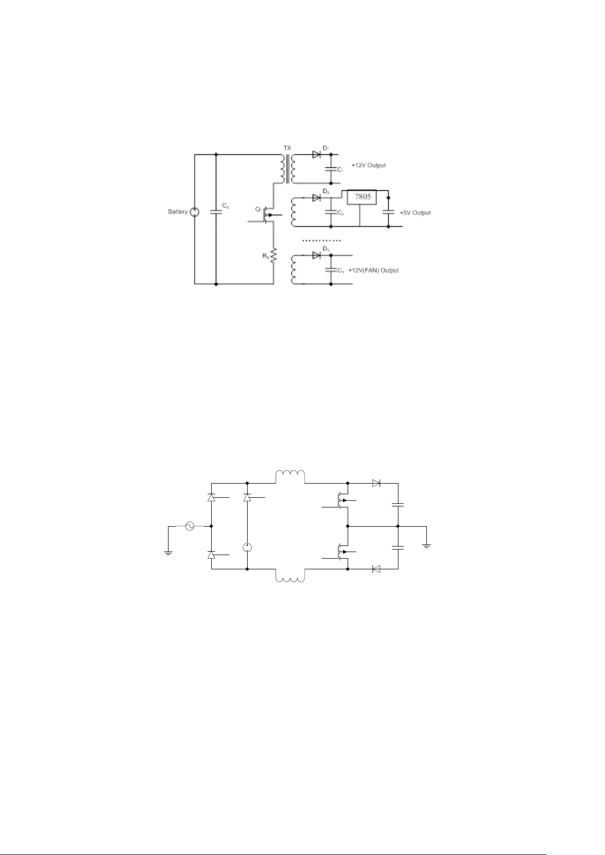
4. Working Principle of the Major Functional Block
N
Q
1
Q
2
U
BUS+
U
BUS-
Utility
Battery
L
1
D
2
D
1
C
1
C
2
N
L
2
Q
3
Q
4
Q
5
4.1 Switch Power Supply
The Switch Power Supply (SPS) supplies DC power for UPS operation. The input source of the SPS is
the grid when the grid voltage is higher than 110V . Or the input source of the SPS is the battery.
Figure 4.1 Basic circuit of power supply
Figure 4.1 is a flyback converter. When Q1 is on, all rectifier diodes (D1/D2/D3) are on open status and
all output capacitors (C1/C2/C3) supply currents to the load. The primary coil of the transformer will
become a pure inductor and the primary current will linearly increase to store energy in the coil. When
Q1 is off, primary current will stop and all rectifier diodes (D1/D2/D3) will turn to “close” status. It will
release the stored energy from the primary coil of the transformer to the secondary coil to supply loads.
At the same time, it will charge output capacitors including 15V, +12V, +5V, +12V(Fan), and HFPW.
The power of 12V, +5V supplies stable voltage to all kinds of ICs and other devices such as HCT. The
+12V (Fan) is supplied to fans and relays. The HFPW supplies a high frequency power for the switch
(SCR/IGBT) driver and some other drive boards.
4.2 PFC/Booster
Figure 4.2 PFC/Booster
As shown in the Figure 4.2, when Q1/Q2 is on and D1/D2 is off, the current will increase to store energy
in choke(L1/L2). When the Q1/Q2 is off and D1/D2 is on, the choke will release energy. Therefore, we
can control the current in chokes (input current) by regulating the time of Q1/Q2 on and off.
4.3 Inverter
The input of the three level inverter topology is two DC voltages, and the output is an AC voltage, as
shown in the Figure 4.3. When Q1/Q2 is on and Q/Q3 is off, the voltage of the bridge midpoint is +BUS.
When Q1/Q2 is off and Q3/Q4 is on, the voltage of the midpoint bridge is –BUS. We can get any voltage
waveform between ±BUS voltage from LC filter output by regulating the duty cycle of Q1/Q2/Q3/Q4,
including sine wave form.
 Loading...