

Page 1
DIGITAL STORAGE
O~CILLOSCOPE
054000
Instruction Manual
-} GOULD
Telephone 01-5001000
Telegrams Attenuate Ilford
Telex 263785
Page 2
Contents
SECTION 1
SECTION 2 Specification
SECTION
SECTION
SECTION 5 Maintenance
SECTION 6
SECTION 7 Guarantee and Service Facilities
Introduction
Operating Instructions
3
3.1 Supplies
3.2 C.R.T. Controls
3.3 Y Channel Controls
3.4 Timebase Controls
3.5 Store Controls 7
3.6 Alias Effects
3.7 Additional Facil ities
3.8
Functional Checks
4
CIRCUIT DESCRIPTION 12
4.1 System Description
4.2 Power Supplies
Y Amplifier
4.3
Analogue-Digital Converter
4.4
4.5 Store and Control Logic
Mode Control
4.6
4.7 Trigger and Timebase
4.8 D-A Converter and Dot Joiner 34
4.9 Calibrator
5.1 General
5.2 Mechanical Assembly
5.3 Fault Finding
5.4 Calibration Procedure
5.5 Wiring details for l00V operation
Circuit Diagrams and
Component Schedules 55
4
Fig. 1
5
6
6
6
6
6
8
9
9
12
13
14 Normal Mode
16
20
27
30 Position
35
36
36
36
39
52
52
79
Fig. 2 Block Diagram of Instrument
Fig.
Fig.
Fig. 5 Timing Signal Waveforms (ADC)
Fig.
Fig. 7 Logic Block Diagram:
Fig.
Fig. 9 Tim ing Diagram: Address
Fig. 10
Fig. 11
Fig. 12 Simplified Control Logic
Fig. 13
Fig. 14
Fig. 15
Fig. 16
Fig. 17
Fig. 18
Fig. 19
Fig. 20 Circuit Diagram: Power Supplies,
Fig. 21 Circuit Diagram: Pre-amplifiers
Fig. 22
Fig. 23
Fig. 24 Circuit Diagram: Timebase
Fig. 25 Circuit Diagram: D-A Converter
Fig. 26
Fig. 27
ILLUSTRATIONS
Alias Effects
3 Block Diagram of ADC
4
Typical Signal Waveforms (ADC)
Timing Chart (ADC)
6
Refreshed Mode
8 Tim ing Diagram: Refreshed
Mode
Sequence
Logic Block Diagram: Roll Mode 23
Timing Diagram: Roll Mode
Timebase Block Diagram:
Bottom View
Righthand View
Righthand View:
Control Condition Table
Data Faults
ADC Waveforms
Y Output and Blanking
Circuit Diagram: A-D Converter
Circuit Diagram: Timing and
Store Logic
and Dot Joiner
Interconnection Diagram 75
Mechanical Views
10
12
'16
17
18
19
20
21
22
24
28
30
37
37
Maintenance
38
40
50
51
57
59
63
69
71
73
77
Page 3
Section 1
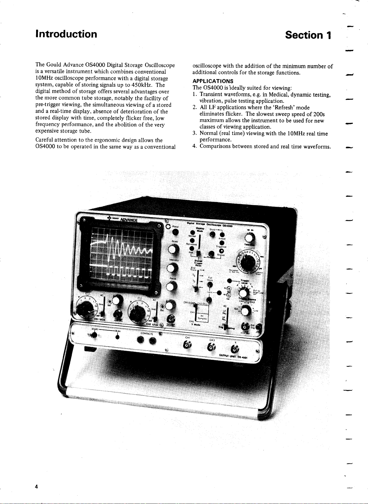
The Gould Advance OS4000 Digital Storage Oscilloscope
is a versatile instrument which combines conventional
lOMHz oscilloscope performance with a digital storage
system, capable of storing signals up to 450kHz. The
digital method of storage offers several advantages over
the more common tube storage, notably the facility of
pre-trigger viewing, the simultaneous viewing of a stored
and a real-time display, absence of deterioration of the
stored display with time, completely flicker free, low
frequency performance, and the abolition of the very
expensive storage tube.
Careful attention to the ergonomic design allows the
OS4000 to be operated in the same way as a conventional
oscilloscope with the addition of the minimum number of
additional controls for the storage functions.
APPLICATIONS
The OS4000 is "ideallysuited for viewing:
1. Transient waveforms, e.g. in Medical, dynamic testing,
vibration, pulse testing application.
2. All LF applications where the 'Refresh' mode
eliminates flicker. The slowest sweep speed of 200s
maximum allows the instrument to be used for new
classes of viewing application.
3. Normal (real time) viewing with the 10MHz real time
performance.
4. Comparisons between stored and real time waveforms.
Page 4
Specification
Section 2
DISPLAY
8 x 10 cm rectangular CRT operating at 4kV
Illuminated graticule
VERTICAL DEFLECTION
Two identical input channels
Bandwidth: DC-lOMHz in the Normal mode
Sensitivity: 5mV/cm to 20V/cm in 12 ranges
Uncalibrated fine gain control gives between
range sensitivity adjustment
Accuracy: ± 3% in calibrated positions
Input Impedance: IM/28pF
Input Coupling: AC-GND-DC
Maximum Input: 400V DC or pk AC
HORIZONTAL DEFLECTION
Timebase: Ills/cm to 20 sec/cm in 23 ranges
Accuracy. - 3%
X Expansion: Continuously variable from IX to 10X
TRIGGER
Source: CHl±, CH2±, Ext±, or line±
Coupling: AC, LF Rej., HF Rej, DC
Sensitivity: Internal 2mm approx., DC-2MHz
Bright Line: Available on normal operation only
. + XJO
with calibrated stops at each end
(lcm at 10MHz)
External IV approx. DC-2MHz
(5Vat 10MHz)
t.s~ ~
"'I{
MCcr~cc;~
iA$~
J-J
a'<er
I SIVV'C/L. ~ ••
k
b
f> ~
FASTEST RISE TIME
For step response:
Maximum Storage 450kHz single trace
Frequency - 3 db: 225kHz dual trace or Alt. Lock
Limited Store: For timebase speeds faster than
Dot Joining: The expanded display appears as straight
ACCESSORIES SUPPLIED
Handbook PN 36240
2 x Lead PL44 BNC-clip
2 x Lead PL43 BNC-BNC
Supplies: Il5V, 220V, 240V ± 10%
45-400Hz, 55W
Size: 17.8 x 31.2 x 41.7 (7" x 12% "x 16*")
Weight: Approx. 11 kg (24% Ib)
Temperature Range: Operating 0 to 50°C
0.551ls
single trace
I.Ills dual trace or Alt. Lock
(Equivalent Bandwidth 600kHz and
300kHz)
SOils/cm
cm is reduced in proportion to the
sweep rate. For speeds slower than
SOils/cm
is reduced in proportion to the sweep
rate
lines joining consecutive samples rather
than as distinct dots
the number of samples per
the maximum stored bandwidth
Full spec. 15 to 35° C
DISPLAY VIA STORE
Store size: 1024 x 8 bits
Vertical Resolution: Approx. 200 for 8cm display, Le.
25 steps per(;m
HORIZONTAL RESOLUTION
Single Trace: Approx. 1000 samples for complete scan
(lOO samples/cm)
Double Trace Approx. 500 samples for complete scan
or Alt. Lock: (50 samples/cm)
Maximum Sample Rate: 1.8MHz
(0.55Ils)
OPTION 4001
This add-on option provides analogue outputs to allow
the trace to be recorded on strip chart, X Y or T Y
recorders and digital outputs for further processing of
the recorded data. (See data sheet.)
Page 5
Operation
Section 3
3.1 SUPPLI ES
The instrument is normally despatched from the factory
with the supply range switch on the rear panel set to the
240V(±10%) range. Check that this is set correctly
before connecting to the supply. Note that the correct
fuse for the two high voltage ranges, 220V and 240V, is
500mA Slo-Blo (20mm) Advance Part No. 33685. If the
115V range is selected the fuse should be changed to a
lA Slo-Blo Advance Part No. 34790.
NOTE:
DO NOT CHANGE THE SUPPLY RANGE SWITCH
WITH THE INSTRUMENT CONNECTED TO THE
SUPPLY.
While the instrument does not rely on forced air
circulation, it should not be operated at elevated
temperatures if the natural connection cooling is
restricted, particularly at the rear of the instrument.
The instrument is switched on by pressing the POWER
button when the associated neon indicator should light.
The button is self locking and the instrument is switched
off by pressing the button agam.
3.2 C.R.T. CONTROLS
These controls are grouped to the right of the c.r.t.
display.
Intensity This is used to set optimum trace intensity
depending on ambient lighting conditions.
Focus Used to obtain finest possible trace width.
Scale The un-illuminated graticule is easily visible
under normal lighting conditions. Graticule
illumination is usually only reqUired under
low ambient light conditions or when photo-
graphically recording the display. The
intensity will depend on the film speed,
aperture and exposure time being used. The
graticule has 0, 10, 90,100% lines marked to
assist in rise time measurement.
3.3 Y CHANNEL CONTROLS
These controls are grouped beneath the c.r.t. display.
The input signal is applied to the CHI or CH2 BNC
input socket.
Coupling
For direct connection of the input signal, set the
associated AC-Ground-DC input iever switch to DC.
For capacitive coupling of the input signal through an
internal O.lpF 400V capacitor, set the lever switch to
AC.
NOTE:
When examining low amplitude a.c. signals super-
imposed on.a high d.c. level, the lever switch should be
set to AC and the sensitivity of the Y amplifier increased.
To locate the baseline, set the lever switch to the 'ground'
setting. At this setting, the input signal is open circuit
and the input of the amplifier is switched to ground.
Sensitivity
Set the VOLTS/CM switch to a suitable setting. To
minimise pick up at sensitive settings, it is essential to
ensure that the ground lead connection is near to the
signal point.
If necessary, adjust the concentric VARIABLE control.
NOTE:
The range of the VARIABLE control is approximately
3.1 so that its.full adjustment overlaps the adjacent
lower sensitivity range. Except at the CAL setting, the
VARIABLE control is uncalibrated. At the CAL setting,
the calibration corresponds to the setting of the VOLTS/
CM switch.
Shift
For vertical shift of the trace, adjust the Y shift controls
(identified with vertical arrows).
Ba!.
The preset balance should be adjusted to minimise
verticle movement of the CHI or CH2 traces when the
inputs are grounded and the attenuator switch is moved
between the 0.5V/cm position and the 0.2V/cm position:
This should only be done after a reasonable warm up
time of say 15 minutes and should only require
infrequent adjustment thereafter.
Y Mode
This three position switch allows single channel display
of the selected channel CHI or CH2, or dual channel
display when CHI&.CH2 is selected.
3.4 TIMEBASE AND TRIGGER
All control~ associated with the Timebase and Trigger
facilities are grouped together on the right hand side of
the panel.
Time/cm, Expand and Shift
The timebase sweep speed (i.e. the time scale of the
horizontal axis) is determined by the setting of the
TIME/CM switch.
X Expand
The time scale can be adjusted to any intermediate
setting by use of the concentric X EXPAND control.
This provides a calibrated sensitivity at the Xl and XIO
detent positions at the ends of travel with a fully
variable uncalibrated range between. The X shift
control, identified with horizontal arrows is used to
centre the display or locate any part of the trace in the
expanded condition. This is a dual action control,
providing fine adjustment over a small angle of rotation
and coarse adjustment over the full rotation.
Trigger
The TRIGGER SOURCE switch selects one of the four
signals, internal CHI, internal CH2, External or line.
The TRIG COUPLING selects wide band DC or AC
coupling.
The AC coupling cuts off at approx. 105Hz.
The L.F. reject position limits the trigger sensitivity
below approx. 15kHz while the HF reject is AC coupled
Page 6
Operation
Section 3
but limits sensitivity above approx. 34kHz. The source
switch also selects the slope, positive or negative going,
to cause trigger when the signal passes through the level
set by the TRIGGER LEVEL control.
The associated L.E.D. indicates when trigger signals are
present. This will flash at low repetition rates and
remain on at faster rates. However it may not indicate
trigger signals above SMHz.
In the Normal mode of operation, the timebase will free
run automatically in the absence of trigger signals.
This provides a "bright line" display to assist in trace
location. With this facility operating, false triggering
may occur if the trigger frequency is less than approx.
40Hz. It is disabled in the Refreshed or Roll modes and
can be disabled in the Normal Mode by pulling the
Trigger Level Knob.
3.5
STORE CONTROLS
All controls associated with the storage facility are
grouped together and distinguished with blue coding.
The DISPLAY MODE lever switch selects the three
modes of operation NORMAL, REFRESHED or
ROLL, the associated L.E.D. indicating the operating
mode.
Normal
In this mode the instrument operates as a conventional
oscilloscope and the store controls do not influence the
display. This mode of operation is available for all
medium and fast sweep rates, O.Ss/cm to IlJ.s/cm, but if
slower sweep rates are selected, the instrument operates
automatically in the Refreshed mode.
Refreshed
If the instrument is displaying a trace in the Normal
mode and the mode switch is moved to REFRESHED,
the display essentially will be unchanged. However in
this mode and in ROLL, the display is generated via the
digital signal path and a small amount of step structure
may be detected on the trace. This is visible in the form
of small vertical steps, less than j6 mm on slow rising or
falling traces. Also with the full X 10 expansion fast
rising or falling traces will appear as a series of sloping
lines (approx. IO/cm in the X direction) rather than as
a smooth curve.
The display is triggered as in the Normal mode but in
the absence of trigger the previously stored trace is
displayed continuously. This has the advantage of
providing a flicker-free display of signals with low
repetition or trigger rates even if a fast sweep is selected.
The display is updated or refreshed by each trigger
signal which would cause a sweep of trace in the Normal
mode. A further advantage over Normal operation is the
availability of very slow sweep rates with continuous
flicker-free display of the sweep as it is written or re-
written.
The Refreshed mode can be used over the full range of
sweep speeds but as the internal sampling rate is limited
to 2MHz, the horizontal sample density decreases in
proportion from the normal lOO/cm when operating at
sweep rates above SOlJ.s/cm.
Roll
Selection of this display mode provides a form of free
running time-base not found on a conventional oscillo-
scop~. Incoming data is fed continuously to the store so
that the display from the store at any instant is a back
history of duration determined by the time/cm speed
control. As the display is continuously updated from
the right, the trace appears to be moving or rolling to
the left similar to the view through a IOcm window of
a strip chart recorder trace.
This mode of display is most suited to direct display of
low frequency signals using comparatively slow sweep
speeds.
As with the Refreshed mode, the Roll mode can be used
on all sweep speed ranges but with limited horizontal
sample density at the faster sweep rates.
Store and Release
These buttons operate in the Refreshed and Roll modes.
Operation of the STORE button in the Refreshed mode
retains any current sweep or the next full triggered
sweep as a stored display, unaffected by subsequent
trigger signals. L.E.D. lamps indicate the single shot
sequence followed. The Armed lamp shows that the
circuitry has been primed by operation of the button.
This lamp goes off and the Triggered lamp comes on
during a sweep. Finally this indication is replaced by
the Stored lamp coming on when the stored sweep is
complete. The sequence and resultant display is similar
to operation of the single shot facility on a conventional
storage oscilloscope after erasing any previous trace. The
OS4000 has no need for an erase facility as the entry of
new data into the store automatically rejects previous
data.
Even in the Stored mode it is possible to use the X
EXPAND control with adjustment of the X shift control
for detailed examination of any part of the trace.
Subsequent operation of the Store button will repeat the
single shot storage cycle, updating the display as
required.
Operation of the Release button will return the
instrument to the Refreshed mode of operation.
Pre-Trigger Storage
The effect of operation of the STORE button in the
ROLL mode depends on the setting of the STORED
TRIGGER POINT SWITCH. With this switch in the top
(End Trace) position, the rolling trace will continue after
operation of the STORE button until a trigger is
received when the display will be frozen. Thus it shows
a full trace of signal prior to trigger, Le. trigger is at the
end of the trace, not at the beginning as on a convention-
al oscilloscope, storage type or otherwise.
Operation of the STORE button at the*trace setting of
the STORED TRIGGER POINT switch allows the
display to roll on for ~ of a sweep beyond the next
trigger. The resultant frozen display shows*of the
trace occuring before trigger and
The actual trigger point on the waveform,*from the
y,.
after trigger.
Page 7

Operation
left hand side of the screen, is shown by a bright-up spot.
It may be necessary to reduce the Intensity setting to
obtain contrast to see this spot.
Selection of thehor
Trigger Point allows the proportion of pre-trigger
display on subsequent storage cycles to be varied
accordingly.
The ability to display a trace of the incoming wave-
form prior to or about trigger, can be used up to sweep
speeds of
For this function, the Roll mode is advantageous on
fast changing signals and at fast sweep speeds. These
present a meaningless display which in the free running
Roll mode but are relevant when stored.
The X EXPAND facility can be used with the X shift
control in this Stored mode for detailed examination of
any part of the trace. It should be noted that the bright-
up dot actually occurs approx. 0.2% of trace before the
actual trigger point and this can be seen as a 2mm
difference on X 10 expand.
The Armed, Triggered and Stored lamps associated with
the STORE button, operate in the Roll mode similarly
to that described for Refreshed. At the End Trace
setting, the triggered state is omitted as the display is
held in the Stored Mode immediately upon receipt of
trigger.
After storage, operation of the RELEASE button will
return the function to Roll. Alternatively further
operation of the STORE button will return the function
to Roll but primed for another storage cycle. In either
case previously stored data has to roll out of the store as
new data is fed in. A new trigger signal will be accepted
only when this mixed display condition has cleared.
Lock Full Store
Operation of the LOCK FULL STORE button prevents
change of the data held in the store. It can be used
usefully in the Roll mode to freeze the display at once
if a feature of interest appears on the screen. Alternat-
ively the store can be locked in the Refreshed or Stored
modes. Subsequently the instrument can be used as a
conventional oscilloscope in the Normal mode but the
original locked display is recalled when returned to the
Refreshed mode. The Lock Full Store button latches
mechanically. To enable the instrument to update the
store as usual the button should be pressed again. An
LED indication warns that the Lock Full Store or Lock
Alternate Samples button is pressed. It should be noted
that movement of function switches after a display has
been locked in the Roll mode, can disturb the display,
particularly shifting the start point of the trace and the
bright up trigger marker spot if relevent. This disturb-
ance is not corrected when the function switch is
returned to Roll.
Lock Alternate Samples
All the store functions described above operate irrespec-
tive of the setting of the 'Y' Mode switch. This is, they
apply equally to the single trace display of CHI or CH2
and the dual trace display of CHI&CH2. This is not
SOJ.Ls/cm,
711
trace position of the Stored
irrespective of the trigger rate.
so for the LOCK ALT. SAMPLES button. When this
condition is applied in the Refreshed mode for single
trace displays (CHI or CH2), the effect is to produce a
dual trace display. One trace is stored and the other
free to follow updating signal inputs. This simultaneous
display of stored and the incoming signal can be used to
compare 'before' and 'now' traces or even to compare
traces taken at different sweep speeds, (once a trace is
stored its display is not altered by the setting of the
Time/cm switch except above
the LOCK ALT. SAMPLES in the dual trace, CHI &
CH2, mode has the effect of freezing the CH2 trace,
leaving CHI free to respond to current signals.
It should be noted that it is possible in this condition to
see a narrow vertical transient appearing on the CH2
trace at the point where the CHI trace is being refreshed.
This effect can be removed by switching from CHI and
CH2 to CHI once CH2 has been frozen.
Once the LOCK ALT. SAMPLES button is pressed, it is
possible still to go from Refreshed to Store and then to
Release to Refreshed with the free trace following the
mode selected, but the frozen trace remaining as when
that lock button was pressed. Operation of the LOCK
ALT. SAMPLES button in the ROLL mode is less
meaningful than in the Refreshed mode. Half of the
display is frozen as before, giving a dual trace effect to
single channel displays or locking CH2 only on dual
trace displays. However the trace continues to move
across the screen from right to left with data lost from
the left appearing at the right.
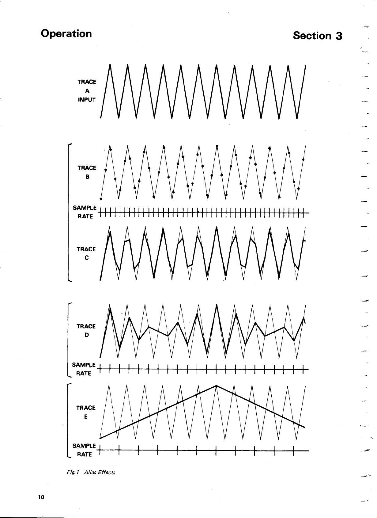
3.6 ALIAS EFFECTS
In the Refreshed and Roll modes, the instrument uses a
sampling system to examine the incoming waveform.
Any such system can give misleading results known as
alias effects if the input signal has a significant
component with a frequency approaching or above the
sampling frequency.
Fig. I shows the effect of the sampling process on a
triangular input waveform (trace A).
Trace B shows the effect of sampling at a frequency
close to four times that of the input if the display is
formed by a series of dots. It will be seen that this can
become a meaningless jumble. However trace C shows
the same sampled waveform reconstructed with the dot
joining system employed in the OS4000. Thus the
display is formed by a series of straight lines, joining the
successive sampled levels rather than a dot at each level,
usually used on reconstructed displays. The dot joining
approach is seen to retain the essential nature of the
input waveform without ambiguity. This is particularly
important as the horizontal dot density is much closer
than that shown on the diagram. However if the
sampling rate is reduced further, the essential nature of
the waveform will be lost. Trace D shows the effect of
a sampling rate close to half the input frequency and
Trace E the effect when the frequencies are nearly equal.
In the latter case the display appears as the input form
but at reduced frequency. The frequency division is the
SOJ.Ls/cm).
Operation of
Page 8
Operation
Section 3
principle on which sampling oscilloscopes operate, and
can cause confusion in this case.
The OS4000 takes approx. 1000 samples per sweep.
These are shared between traces on dual channel or
alternate locked modes of operation. Assuming that the
sampling rate should exceed the input signal frequency
by a factor of between 4 or 5, the following table shows
the maximum frequency which can be viewed on each
range.
Dual Channel
Time/cm Range Single Channel or Alt. Locked
50 Ils/cm 400kHz 200kHz
O.lms/cm 200kHz 100kHz
0.2ms/cm 100kHz 50kHz
0.5ms/cm 40kHz 20kHz
1 ms/cm 20kHz 10kHz
2 ms/cm 10kHz 5kHz
5 ms/cm 4kHz 2kHz
10 ms/cm 2kHz 1kHz
20 ms/cm 1kHz 500Hz
50 ms/cm 400Hz 200Hz
0.1 s/cm 200Hz 100Hz
0.2 s/cm 100Hz 50Hz
0.5 s/cm 40Hz 20Hz
1 s/cm 20Hz 10Hz
2 s/cm 10Hz 50Hz
5 s/cm 4Hz 2Hz
10 s/cm 2Hz 1Hz
20 s/cm 1Hz 0.5Hz
At sweep speeds faster than SOils/cm the sampling rate
remains at 1.8MHz and the storage capability is reduced.
Thus the usable frequency remains at 400Hz or 200kHz.
In practice there is little advantage is using the storage
modes above SOils/cm.
The above table shows the order of frequency which can
cause mis-Ieading displays. The actual amount of
distortion depends on both the frequency and the wave-
shape involved. Individual peaks of sinusoidal signals
can be -3db at a frequency approx. 10% above those
shown above.
If alias effects are suspected, it is recommended that the
fastest possible sweep speed is selected. Repetitive
signals are best viewed in the normal mode if possible,
before comparison with a refreshed trace.
It should be noted also that the sampling system will
not detect narrow transients which occur between
samples.
3.7 ADDITIONAL FACILITIES
Cal
These pins provide d.c. coupled positive-going square
waves of 0.1V and 1V ± 2% amplitude at approximately
1kHz frequency for calibration checks, (2kHz when
Time/cm set SOils/cm or faster). Shorting between the
CAL pins will produce a square current wave-form of
ImA in the shorting link. This can be used for current
probe calibration.
Use of Optional PassiveProbe
A x 10 passive probe may be used to extend the voltage
range and increase the input impedance of the Yampli-
fiers. The input resistance of a Y channel is 1MD
shunted by approximately 28pF. The effective capacity
of the input lead must be added to this and the resultant
impedance will sometimes load the signal source. There-
fore it is advisable to use a lOMD, x 10 probe. This
reduces the input capacity and increases the input
resistance, at the expense of the sensitivity. The probe
contains a shunt RC network in series with the input,
and forms an attenuator with the input RC of the Y
channel. To obtain a flat frequency response it is
necessary to adjust the capacitance of the probe to
match the input capacity of the Y channel as follows:-
1. In the Normal Mode, set the Y channel VOLTS/CM
switch to 20mV/cm, and the TIME/CM switch to
.2ms/cm.
2. Connect the probe to the CAL 1V pin.
3. Set the adjustable capacitor in the probe tip or
termination with a small screwdriver for a level
response with no overshoot or undershoot visible
on the display.
3.8 FUNCTIONAL CHECKS
This section describes a test routine which checks that
the instrument is functioning correctly in its main modes
of operation, but it also provides examples of how to set
and use the instrument.
Normal Mode
Switch on, put Display Mode switch to normal.
Put timebase switch to Ims/cm; CHI and CH2
attenuators to 0.2V/cm; Trigger Lever Control knob
pushed in; CHI, CH2 and X shift controls central;
Y Mode switch to CHI
switches to GND; Trigger source switch to CHI; Trigger
Coupling to A.C.
Turn Intensity control to clockwise end. Adjust CHI
and CH2 shift controls to obtain two traces. Adjust
Intensity and Focus control to obtain finest possible
traces.
Rotation of the Trigger Level control through the
central position will cause trigger L.E.D. to flash once.
After about 15mins. warm up, check that on both
channels the vertical trace movement caused by turning
the attenuator switches from 0.2V/cm to 0.5V/cm is less
than 0.5cm. If not adjust the BAL. pre-set for that
channel. Set input coupling switch to DC.
Apply sine wave at approx. 1kHz to CHI and select
CHI as trigger source. Adjust CHI attenuator and/or
signal amplitude to give about 5cm Y deflection. Adjust
level control to obtain stationary trace - check trigger
L.E.D. is illuminated. Pull out Trigger level control to
disable Bright Line facility and turn until trigger is lost;
trace should disappear. Trace should re-appear free
running when Level control is pushed in. Reset Level
control for stationary trace.
&
CH2; Input coupling
Page 9
Operation
TRACE
INPUT
TRACE
SAMPLE
RATE
Section 3
A
B
TRACE
C
TRACE
o
SAMPL.E
RATE
TRACE
E
SAMPLE
RATE
Page 10
Operation
Section 3
Refreshed Mode
Apply approx. 1kHz with the timebase on the O.5ms/cm
range. Obtain a stable display. Switch the Display mode
to Refreshed. The Display is now being obtained from
the store. Removal of the signal by disconnecting the
input or switching the input coupling switch to the CND
will cause the last "sweep" to be preserved in the store
and displayed indefinitely. This sweep may include the
break of signal. Apply a 1 to 10Hz sine wave and adjust
the timebase range switch accordingly. Adjust the level
control to light the trigger L.E.D. The refreshing sweeps
through the store can be clearly seen as the time base
range is switched up or down.
Store
If the signal is removed and the Store button pressed, on
re-applying the signal the sequence-trigger-store can be
followed by watching the status indicators, and the store
will have been completely updated when the store
L.E.D. is lit. The sequence may be repeated by pressing
the Store button again.
Lock Full Store
Select CHI only, with CHI as trigger source. Apply
approximately 1kHz signal and adjust the Trigger Level
so that refreshing sweeps are occuring. Push Store
button and when the store L.E.D. is lit, push the Lock
Full Store button. On returning the Display mode
switch to the normal position, conventional oscilloscope
operation is possible - Le. the input attenuators and
time base range can be altered, another signal can be
observed, but on returning the mode switch to the
Refreshed position, the original stored display will be
obtained, irrespective of the current input and setting of
the sensitivity and sweep speed controls
slower). Release the Lock button.
Lock Alt. Samples
With the display mode switch in the refreshed position
again, apply the same signal as before and adjust trigger
level to obtained refresh sweeps. Store the trace then press
the Lock Alt. Samples button. On returning to the
refreshed mode (pushing Release button) it will be
found that operating the CHI shift control, results in
two traces being generated - one which responds to the
input signal, shift, attenuator and timebase controls, the
other a fixed display of the original store contents. On
uplatching the Lock ALT. Samples button a single trace
is again displayed.
(SOils/cm
or
Select CHI & CH2 (Dual trace), CHI trigger, and
apply approximately 1kHz signals to CHI and CH2.
Adjust trigger level so that refresh sweeps are occuring.
Push Store button and wait for store L.E.D. to light. If
the Lock Alt. Samples button is operated on returning
to the refreshed mode, one trace (CHI) will respond to
the CHI shift and input signal, the other trace (CH2) is
locked. Returning to the normal mode will not destroy
the CH2 information held in the store until the Lock
Alt. Samples button is un-latched.
Roll Mode
Switch display mode to Roll. Select a low sweep speed
such as 1 sec/cm. Select CHI only. Offset trigger level
to one end, and check Hold and store L.E.D.'s are off.
Movements of the CHI shift control will now be seen to
draw a trace on the screen similar to a strip chart
recorder, with the "pen" at the right hand side of the
screen, and the trace moving towards the lift at the
sweep speed selected. This movement can be arrested at
any time by pressing the Full Lock button.
Pre-trigger Storage
Apply a low frequency signal of approximately 1Hz and
with trigger coupling in the D.C. position adjust the
trigger level control until the trigger source L.E.D.
flashes continuously. The display will continue to move
to the left. Remove the signal and press the Store
button. On re-applying the signal the sequence,
triggered-stored will be followed resulting in a stationary
display. The length of time spent in the triggered
condition and therefore the final waveform position is
dependent upon the setting of the stored trigger point
switch, and can be changed from zero to three quarters
of the full sweep time. At normal to low settings of the
brilliance control a bright dot can be observed marking
the point of trigger (it is displaced approximately 0.2 cm
on XIO expansion to the left of the true trigger point).
After a stationary display has been obtained, if the signal
is not removed, but its frequency is changed by say 2: 1,
on pressing the store button again, the sequence,
triggered-stored will be followed, resulting in a stationary
display again. It will be found that the new display
contains none of the "old" frequency, because the
store will automatically take in just enough new
information before becoming sensitive to trigger such
that the next stored waveform consists of new
information entirely.
Page 11
Circuit Description
Section 4
4.1 SYSTEM DESCRIPTION
With the MODE switch in the NORMAL position the
instnnnent operates in a conventional manner. Referring
CH' CH' ATTENUATQR
'ip PRE AMPLIFIER
CH2 CH2 ATTENUATOR
!/p
AND
AND
PRE AMPLIFIER
TRGGER
AMPLlRER
can hold 1024 such 8 bit words and the data is entered
at a rate such that the information contained in the
whole store represents one complete sweep. This data is
to fig.2., input signals are applied to two identical pre-
amplifiers which incorporate the sensitivity controls,
both variable and switched, and also the Y shift and in-
put coupling controls. The outputs of these pre-
amplifiers are applied to the beamswitch and also to the
trigger selector switch. The beamswitch selects one or
other of the two channels and on dual trace, is operated
either in a chopped or alternate sweep mode, dependent
on the setting of the timebase range switch. The output
of the beamswitch is applied via the signal switch to the
Y output amplifier which drives the vertical deflection
plates of the C.r.1. A trigger signal is selected by the
trigger selector switch and shaped into fast pulses by the
trigger amplifier which contains the trigger level, slope
and coupling controls. These trigger pulses are supplied
via the control logic to the time base and initiate a linear
ramp, the duration of which is determined by resistors
and capacitors switched by the time base range switch in
the usual manner. This ramp is applied via the X ampli-
fier to the horizontal deflection plates of the c.r.t. A
bright line facility is available such that when no trigger
signal is being received, the timebase is made to free run,
producing a visible base line.
When the MODE switch is in the REFRESHED position,
the signal switch is changed over so that the output from
the Dot Joiner is routed to the Y output amplifier.
Analogue signals from the beamswitch are applied to the
Analogue to Digital Converter (ADC) which produces an
8 bit binary code (word) representing the instantaneous
signal level at 550 nanosecond intervals.
The data produced by the ADC can be loaded into a
store under the control of the timing logic. The store
then continuously read out (non-destructively) at a fixed
rate and reconstituted as an analogue signal by the
Digital to Analogue Converter (DAC), and applied to the
Y output amplifier to give a continuous display of the
store contents. Since the output from the DAC is in the
form of discrete levels, a dot joiner is included to join up
these levels and provide a continuous display.
The time base section provides continuous sweeps at a
fixed rate of lOOlls/cm irrespective of the setting of the
timebase switch, and synchronised to the store read out
cycle.
Note that the trigger amplifier is now entirely dissociated
from the timebase since the latter is running continuously.
The function of the trigger amplifier is to initiate a read-
in cycle, when a screen full of new information will be
entered into the store. The rate at which new data is
entered determines the effective time base rate of the
viewed signal; the 1024 available store locations represent
approximately 11.3 cms. of trace length, thus there are
91 samples per cm. A data entry rate of 0.91 MHz would
correspond to 100Ils/cm. and 91 Hz to Is/cm. and so on.
The data entry rate is determined by a programmable
digital divider controlled by the time base range switch.
This divider operates on the basic clock frequency of
1.82MHz which corresponds to SOils/cm, the fastest
sweep rate available in the digital mode.
Dual trace operation in the REFRESH mode is catered
for by operating the beamswitch in the chop mode at
half the data entry rate, thereby storing samples of each
trace in alternate store locations. Since the store is being
read out at a relatively fast rate, however, the alternate
sweep technique is used during read out, with store
Page 12
Circuit Description
Section 4
locations relevant to one trace being read out on one
sweep, and the remaining location on the next sweep.
The STORE control provides a conventional single shot
facility to enter one triggered sweep of data into the store,
while the LOCK STORE controls inhibit immediately
the entry of any new data.
The ROLL mode of operation is similar to the
REFRESHED mode except in the way in which new
data is entered into the store. Instead of waiting for a
trigger pulse to initiate a new data input cycle, data is
continuously entered into the store. Thus, if data entry
is made to stop on receipt of a trigger pulse, the contents
of the store will be information stored before the trigger
pulse, rather than after it as in a conventional trigger
sequence. To expand this facility, which operates only
in conjunction with the single shot store controls, a
switched delay is incorporated marked STORED
TRIGGER POINT which allows the input of new data
to continue after a trigger is received, for a time corres-
ponding to ~, ~ or%of the store length. This allows the
amount of pre-trigger and post trigger information
retained in the store to be varied to suit the application.
Circuit References
Each component in the instrument is specified by a
circuit reference consisting of a letter prefix and a
number. The number also indicates which printed
circuit board assembly the component is mounted on
as shown below:-
Circuit Reference No.
o -
99 Main Frame Components
100 - 399 Analogue to Digital Converter
Assembly
400 - 499
500 - 599
600 -699
700 - 799
800 - 899
900 - 1099 Timebase Board.
The location of the various assemblies is shown in
Figs.14, 15 and 16.
4.2.1
GENERAL
Referring to Fig.20 all the power supplies for the
instrument are derived from the transformer, TS1. Two
tapped primary windings are switched by SS2 to allow
for three supply voltage ranges and fuse FSS1 provides
fault protection. The supply indicator neon, NE 51, is
supplied via limiting resistor RS8 from the 115 volt tap
on the transformer.
4.2.2
LOW VOLTAGE SUPPLIES
Five separate secondary windings supply bridge rectifiers,
BRS1-BRSS, mounted on the transformer and provide
unregulated supplies of +170V, +26V, -26V, +18V,
-lOV and +8V across the reservoir capacitors, CS09A,
E.H.T. Board
Power Supply Board
Store Logic Board
Timing Logic Board
Output Unit 4001 - Fitted as
an option. See separate handbook
for details.
CS10, CS11, CS12, CS02 and CS1 , respectively. Note
that the -10V and +8V supplies are floating with respect
to ground due to the action of the regulators. The +170V
supply is further smoothed by RS40 and CS09B and
protected by fuse, FSS01. The + 26V, -26V, + 18V and
-10V supplies are fed to high performance integrated
circuit regulators, ICS03, ICS04, ICS01 and ICS02
respectively to provide stabilised lines of +20V, -20V,
.+12Vand -6V. These devices contain all the circuitry
necessary for a conventional series regulator, together
with current limiting and thermal shutdown facilities to
protect the device against overloads arising from short
circuits, etc. Note that the two 20V lines are in fact
provided by lSV regulators in conjunction with zener
diodes, DS03 and DS04.
The +8V supply feeds a discrete series regulator com-
prising transistors, TRSOS-TRS10, and associated
components, to provide a stabilised +SV line. The long
tailed pair, TRSOS and TRS06, compares the output
voltage with the voltage across the zener diode, DSOS,
and provides an error signal which is passed via the
emitter follower, TRS09, to the series pass transistor,
TRS10. A second long tailed pair, TRS07 and TRS08,
senses the voltage drop across the current sensing
resistor, RS22, and if the supply current rises above
3 amps will shut down the regulator by reducing the
reference voltage at the base of TRSOS. The resistor
network, RS18, RS17 and RS20, determines the
limiting current and also provides a 'foldback' limiting
characteristic by reducing the permissible output current
of the regulator as the output voltage falls. This prevents
excess dissipation in the series pass transistor under short
circuit conditions. The zener diode, DS06, prevents the
output voltage of the regulator rising excessively high
under fault conditions and thus protects from damage
the integrated circuits supplied from this line.
4.2.3 E.H.T.
The two remaining secondary windings are associated
with the cathode ray tube (c.r.t.) supplies. The 6.3V
winding feeds the c.r.t. heater and the 850 volt winding
provides the -lkV and the +3kV supplies. Stabilisation
of both lines against supply voltage variations is achieved
as follows. One end of the 8S0V winding feeds the
rectifier diodes in the normal manner, the other end
passes to ground via a bridge rectifier, BR401. The alter-
nating current in the winding passes through R406 and
TR402 as direct current developing a steady voltage
across C402. This voltage, controlled by the conduction
of TR402, is effectively subtracted from the peak voltage
available at the 'hot' end of the winding and thus by
varying the base-emitter voltage of TR402, the rectified
high voltage supplies can be controlled. The average value
of the base-emitter voltage of TR402 is established by the
voltage at TR403 emitter. This in turn is controlled by
the voltage at TR403 base set by the feedback resistor, R411,
from the -lkV supply line and the combination of R409
and R41O, thus establishing a closed feedback loop. A
small current also flows from the base of TR403 via R407
SUPPLIES
Page 13
Circuit Description
Section 4
to the unregulated -26V supply. Since this voltage
changes with the line voltage, this trims out any remaining
fluctuations in the E.H.T. supplies due to supply variations.
The -lkV supply is derived by the diodes, D404, D405
and D406, feeding the reservoir capacitors, C404, C407
aqd C406. The voltage is smoothed by R413, R414 and
C405, C408 and C409 and applied to the grid of the c.r.t.
The cathode potential of the tube is held positive w.r.t.
the grid as determined by the brilliance control, R419,
and the second anode potential is set by R416 to opti-
mise the focus. Small positive voltages set by R417 and
R408 are applied to the third anode and interplate shield
to minimise raster distortion.
4.2.4
GRATICUlE IllUMINATION
The graticule is illuminated by two lamps, ILPI and ILP2.
The supply for these lamps is derived from the emitter
follower, TR401, and controlled by the potentiometer,
R402. This circuit is supplied from the 8 volt winding
of the transformer via diodes, D53 and D54.
4.2.5
THE TRACE ROTATION COil
A coil, L51, fitted round the neck of the C.r.t. inside the
magnetic shield, is used to align the trace with the
horizontal graticule lines. The current for this coil is
taken from the pre-set potentiometer, R529, through
R530 on the power supply board. The direction of
rotation can be reversed by interchanging the coil
connections at the power supply board.
4.3.1
THE Y PRE-AMPLlFIER
The attenuator and pre-amplifier in Channel I are
identical to those in Channel 2. Accordingly only
Channel I will be described. Referring to Fig.21 the
input signal is applied to the front panel socket, SKY,
and then to the 3 position lever switch, SI, via R22.
This switch selects AC or DC inpuLcoupling by including
or by-passing C20 in the signal path. On the middle
position of the switch, the input socket is disconnected
and the input to the amplifier is connected to ground.
Input sensitivity selection is performed in two stages; the
six lowest ranges, 5-200mV/cm, are obtained by switch-
ing the gain of the amplifier as described later. The 0.5-
20V/cm ranges are provided by switching in a -;.-100
attenuator section before the amplifier and repeating the
gain switching. This attenuator is formed by R24 and
R351 with C305 to set the hJ. response. C303 is adjusted
to maintain the total input capacitance of the highest
ranges equal to the lower ranges. Diodes, D301 and D302,
limit the peak signal voltage at the amplifier input to
approximately 8 volts and in conjunction with R26,
protect the instrument against damage from inputs of up
to 400 volts peak.
The input stage consists of the field effect transistor,
TR30 I, connected as a source follower driving the emitter
follower, TR305, via R303. The operating current of
TR30 I is defined by TR302 which is an identical transis-
tor mounted in a common package with TR301 to ensure
close matching and good thermal tracking. TR302 is self
biased such that the operating current will develop a
voltage across R308 equal to the gate-source potential.
Since this same current flows in TR301 and R303 is
identical to R308, the voltage at the base of TR305 is
equal to the gate voltage of TR30 1. The drain-source
voltage of TR301 is maintained constant by 'boots-
rapping' with TR304 and D303. The drain-source
voltage of TR302 is also maintained constant by the
cascode transistor, TR303. Diode, D304, prevents the
base-emitter junction of TR305 becoming reverse biased
under overdrive conditions. The voltage at the gate of
TR302 can be varied by R373 to balance out small
variations in matching characteristics.
The signal at the emitter of TR305 is applied via the
switched resistor network, R28/34, and the common
base stage, TR306, to the shunt feedback amplifier
formed by TR307, R312 and R311. This can be
regarded as a 'virtual earth' amplifier with R311 as the
feedback resistor and the R28/R34 network as the input
resistor. Thus, the overall gain of the stage is selected by
S3B to provide the six basic input sensitivities of the
instrument. The common base transistor, TR306, is
interposed to balance the d.c. offset voltage introduced
into the signal path by TR305. Diode D305 is fitted to
protect TR306 from reverse base-emitter voltages. The
output from the collector of TR307 is taken via R315 to
the base of TR309, which, together with TR31O, forms
a long-tailed pair. Transistors, TR315 and TR308, are
connected in a similar fashion to TR306 and TR307 and
provide a balancing d.c. voltage at the base of TR31O.
The mutual conductance of the long-tailed pair is deter-
mined by series combination of R319, R320 and R3.
Resistor, R3, is the variable sensitivity control and is
shorted by S13 when in the 'CAL' position. The preset
potentiometer, R319, sets the overall gain of the pre-
amplifier and C309 provides h.f. compensation.
Movement of the displayed trace will occur when the
variable sensitivity control, R3, is operated unless the
voltages at the emitters of TR309 and TR31 0 are equal
(except for the input signal) and this balance is set up
using potentiometer, R369. The collector current of
TR309 feeds into a load resistor on the time base board
to provide an internal trigger signal.
4.3.2
BEAM SWITCH
The collector current from TR310 is passed through a
cascode transistor, TR317, to the emitter of the beam
switch transistor, TR319. A d.c. current determined by'
the shift control potentiometer, RI, and the series resistor,
R387, is injected at the emitter of TR317 to provide a
shift range of ±12 cms. If the base of TR319 is held high
(approx. 3.3 volts) the signal current will pass through the
forward biased diodes, D313, D315 and D316, to the load
resistor, R389. If the base voltage of TR319 is low
(approx. 0.4 volts) the signal current will flow through
TR319 to ground and D313 will become reverse biased
isolating Channel I from the common load resistor, R389.
An identical beam switch circuit controls the output of
Page 14
Circuit Description
the Channel 2 pre-amplifier but the drive to transistor,
TR320, is the complement of that to TR319.
For dual trace operation the beam switching technique
employed depends upon the main operating mode switch.
In the NORMAL mode the channels are switched on
alternate sweeps when the time base range switch is set
to 2 msec./cm. or faster. On the lower timebase ranges
the beam is chopped at a 225kHz rate. In the
REFRESHED and ROLL modes the channels are always
chopped at a rate dependent on the setting of the time-
base range switch. On the 50p.sec./cm ranges and above,
the chopping rate is 0.9MHz; below this the chopping
rate decreases pro rata Le. at 5msec./cm, it is 9kHz and
at 5 seconds/cm. it is 9Hz.
4.3.3
SIGNAL SWITCH
The combined input from both channels appears across
R389 at a level of approximately 37mV/cm. This signal
is taken via R201 to the Analogue to Digital convertor
(section 4.4) and also via emitter follower, TR321, to
the signal switch formed by diodes, D317 to D320.
This determines whether the signal passed to the Y out-
put stage is the direct signal from the pre-amplifiers
(NORMAL mode) or the stored signal from the Digital
to Analogue convertor (REFRESHED and ROLL modes).
In the NORMAL mode, transistor TR324 is turned off
and its collector is at a high level thus turning TR325
fully on. The voltage at the junction of diodes D319
and D320 will be low and both diodes will be reverse
biased. The two diodes, D31 7 and D318, will be forward
biased and conducting however, and a signal at the
emitter of TR321 will be transferred to the junction of
D318 and D319, and via R379 to the Y output stage.
When a high level is applied via R362 to the base of
TR324, this transistor is turned on, TR325 becomes cut
off and the situation is reversed with D317 and D318
reverse biased and the signal from TR322 emitter trans-
ferred to the output stage. The stored signal from the
Digital to Analogue convertor is applied via R355 to the
base ofTR322. To compensate for the dc level shift
introduced into the signal path by the emitter followers,
TR321- TR322, a bias supply is provided for the output
stage by transistor, TR323, which is operating under
quiscent conditions identical to transistors, TR321 and
TR322. The collectors of all these three transistors are
supplied via R391 and clamped by D321 to approximately
-0.7V in order to reduce dissipation in the devices.
4.3.4 Y
OUTPUT AMPLIFIER
The Y output amplifier shown in Fig.20 is a conventional
two stage differential amplifier. Input signals from the
signal switch are applied via SK.U to the base of TR409
and a bias signal at the same d.c. level (approx. +0.6 volt)
is fed to the base of TR408. These two transistors form
a long-tailed pair with the gain determined by the resistor
combination, R437 and R438, in conjunction with the
collector load resistors, R441 and R442. The two
resistor-capacitor combinations, R443, C424, C426 and
R448, C430 provide pulse response correction. The
zener diodes in the collectors, D411 and D412, set the
collector-emitter voltage across each transistor so that
variations in-power dissipation (and hence junction
temperature) of the transistor with signal amplitude, are
minimised. The output signal from this stage is applied
to the bases of a second long-tailed pair, TR406 and
TR407, which are connected in cascode configuration
with TR404 and TR405, respectively.
The c.r.t. deflection plates are driven from the collectors
ofTR404 and TR405 with inductors,
UOl
and
U02,
providing shunt compensation. The networks, C419,
C420, R425 and C421, R427 across the gain setting
resistors, R426 and R435, provide h.f. compensation to
ensure good pulse response.
4.3.5
BLANKING AMPLIFIERS
There are two separate blanking amplifiers producing
intensity modulation of the c.r.t. display and these
operate with three separate input signals viz:
i) The Sweep Blanking signal. This cuts off the beam
except when a time base sweep is in progress.
ii) Chop Blanking. This is a short duration blanking
pulse applied in the NORMAL mode only when the
beamswitch is being switched from one channel to
the other at the fast chopping rate.
iii) Trigger Point Bright-Up. This is a short duration
bright-up pulse applied once per sweep when a
trace has been stored in the ROLL mode of
operation.
The Sweep Blanking signal is amplified by a d.c. coupled
amplifier comprising TR513 and associated components.
The sweep blanking signal is derived from a TTL. logic
gate (IC902a) in the timebase via R971 (see Fig.24).
When no sw.eep is in progress the sweep blanking signal
is at a low level «0.4 volt) and transistor TR513 is cut
off. The collector voltage in this condition is determined
by the resistor chain, R526, R527 and R528, at approx.
90 volts. This voltage is applied to the second grid elec-
trode (blanking electrode) of the c.r. t. and the beam is
cut off.
When a sweep is initiated the sweep blanking input from
the timebase rises to a high logic level (approx. 4 volts)
turning on transistor TR513. The base drive to this
transistor is limited by D507 becoming forward biased
to avoid saturating the transistor and the collector
voltage falls to 4 volts, thus unblanking the C.r.t. beam.
The remaining two input signals are amplified by the
circuit comprising TR514, TR515 and TR516. Both
the Chop Blanking (CB) and Trigger Bright-Up (TBU)
signals are produced by TTL logic devices situated on
the Timing Logic board and the Store Logic board
respectively (see Fig.23). For detailed information on
the timing of these signals see section 4.5
The Trigger Bright-Up signal is inverted by the common
emitter stage, TR514, and applied to the base ofTR515
via R508. The Chop Blanking signals are applied directly
to the base of TR515 via R507 and the speed-up capacitor,
C505. The signal at the collector ofTR515 is fed to the
base of TR516 via the d.c. level-shifting network, D508
and C519. The pulses occurring at the collector of
Page 15

Circuit Description
Section 4
TR516 are a.c. coupled to the grid of the C.r.t. by C506.
The resistor, R533, serves to isolate the c.r.t. grid from
the relatively low output impedance of the power supply
and the clamping diode, D509, prevents the grid from
being driven positive w.r. 1. the supply, and thus possibly
positive W.r.t. the cathode.
4.4.1
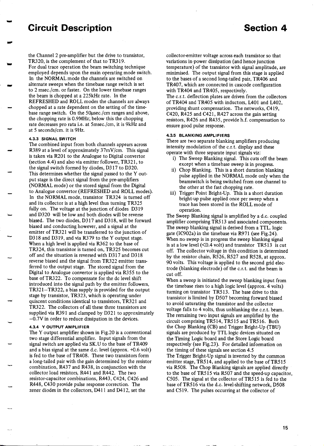
BLOCK DIAGRAM DESCRIPTION
The function of the Analogue to Digital Convertor (ADC)
in the summing amplifiers. Typical waveforms are shown
in Fig.4.
This process is then repeated using a row of 7 compara-
tors to decode the next 3 bits of data and a further DAC
and summing amplifier to drive the final row of 7 corn-
patators.
4.4.2
SCALING AMPLIFIER
Referring to the circuit diagram Fig.22 the analogue input
signal from the beamswitch is applied via R20 I to the
base of TR201. TR201 and TR202 are a Darlington
is to quantise the instantaneous signal magnitude into one
of 256 levels. These levels are represented by an 8 digit
binary code (8 bit word) and the conversion is performed
once every 550 nanosec.
Referring to the block diagram Fig.3 the input is applied,
via a scaling amplifier, to a sample-and-hold circuit. This
samples the signal level every 550nSec. and presents this
level to the first row of comparators. These compare the
signal against 3 fixed voltage levels corresponding to Y<!,
%
and*full scale input voltage. The output states of
these three comparators are then decoded to give the
first two most significant bits of the output data, DI and
D2. A 'remainder' signal is produced by subtracting from
the original signal the voltage represented by the two bits
already decoded. This operation is performed by a
summing amplifier, AI, and a 2 bit Digital to Analogue
Convertor (DAC). The reference volt ages for the
comparators are generated by the precision resistors, R,
and the current source,
exactly to the voltages subtracted from the input signal
n.
These voltages correspond
connected pair which, together with TR203 and TR204,
form a conventional long-tailed pair amplifier. The out-
put signal is taken from the collector of TR203 via the
emitter-follower, TR205, and fed to the base of the
sample-and-hold input transistor, TR206. The gain of
the scaling amplifier (approximately x12) is determined
by applying negative feedback via the potential divider
network, R2II, R207 and R208. Potentiometer, R217,
and resistor, R209, introduce a d.c. offset into the
amplifier output by drawing current through the feed-
back network. The diodes, D215 and D216, are normally
reverse biased and clamp the output signal of the amplifier
to within the working range of the ADC.
4.4.3
SAMPLE·AND·HOLD
The signal from the scaling amplifier is presented via the
emitter follower, TR206, to the sampling transistor,
TR208. This is a junction f.e.t. and it's gate is controlled
by the monostable circuit formed by TR209, TR207,
TR210 and TR212.
Page 16
Circuit Description
INPUT
SIGNAL
Section 4
I
I
I
I
I I
----------------~--------~
I
I I
I I
I I
I I I
I
1st.ROW
COMPARATOR
LEVELS
--+----------------t--------~-
I
FIRST
TWO
DATA
BITS
,
I
_n _
I
I
I
I
I
OUTPUT
FROM
FIRST
SUMMING
AMPLIFIER
The sample-and-hold cycle is initiated by a timing pulse
from the ADC logic board applied to the base of emitter
follower, TR226. This is amplified by the common
emitter amplifier, TR227, and differentiated by C214.
The negative going edge of this pulse appears at base of
TR209 and turns off the transistor. The collector
voltage of this transistor rises and turns on TR21 0 via
emitter follower, TR207, and the potential divider,
R222, R226. The negative-going signal at the collector
of TR21 0 is fed back via emitter follower, TR212, D207
and C212 to the base of TR209 thus maintaining the
L
I
I
I
I
I
I
- 2nd.1UN
- COMPARATOR
-}
- LEVELS
circuit in this state until C212 charges up via R218, and
TR209 turns on again.
In this way a large positive-going pulse, approximately
lOOnSec. long, appears at the gate of TR208. During
this time TR208 conducts and charges C210 to the input
signal voltage present at the emitter of TR206. The
injection effect of the gate-drain capacitance in TR208
is compensated by driving TR211 gate with the inverse
of the signal fed to TR208 gate. Similarly the drain-
source capacitance of TR208 is balanced by an antiphase
signal applied via C206. The voltage stored across C210
Page 17
Circuit Description
is buffered by a voltage follower comprising TR213,
TR214 and TR215. TR213 is a source follower driving
the emitter follower, TR215. The operating current of
TR213 is defined by an identical transistor, TR214,
operating in a manner similar to the Y Pre-Amplifier in-
put stage as described in section 4.3. The low impedance
output at the emitter of TR215 is fed to the first row of
comparators, ICIII and ICII2, and also to the first
summing amplifier, ICI02a.
4.4.4 COMPARATORS AND DECODING LOGIC
The comparators are very high gain integrated circuit
differential amplifiers. The signal is applied to the non-
inverting input and a reference voltage to the inverting
input. If the signal voltage is less than the reference
voltage the output of the comparator will be at its low
limit. When the signal rises above the reference voltage
the output goes to its high limit. The gain of the device
is sufficiently high to ensure that the output will be at
one limit or the other under most practical circumstances.
The reference voltages for the comparators are generated
by chains of precision resistors, R266-R268, R278-
R284 and RI46-RI52, in conjunction with constant
current source circuits. Since the digital to analogue
convertors shown in the block diagram also employ
current sources, these are grouped together and described
later.
The outputs of the comparators are taken to the de-
coding logic. This provides binary coded output data
corresponding to the state of the comparators, and is
implemented with standard 74 series T.T.L. integrated
circuits. Since the signal applied to each row of
comparators is dependent on the state of the previous
row, the full 8 bit conversion is carried out in a 'ripple
through' fashion with a time lag between each of the
three sections to allow for the settling time of the
comparators and summing amplifiers.
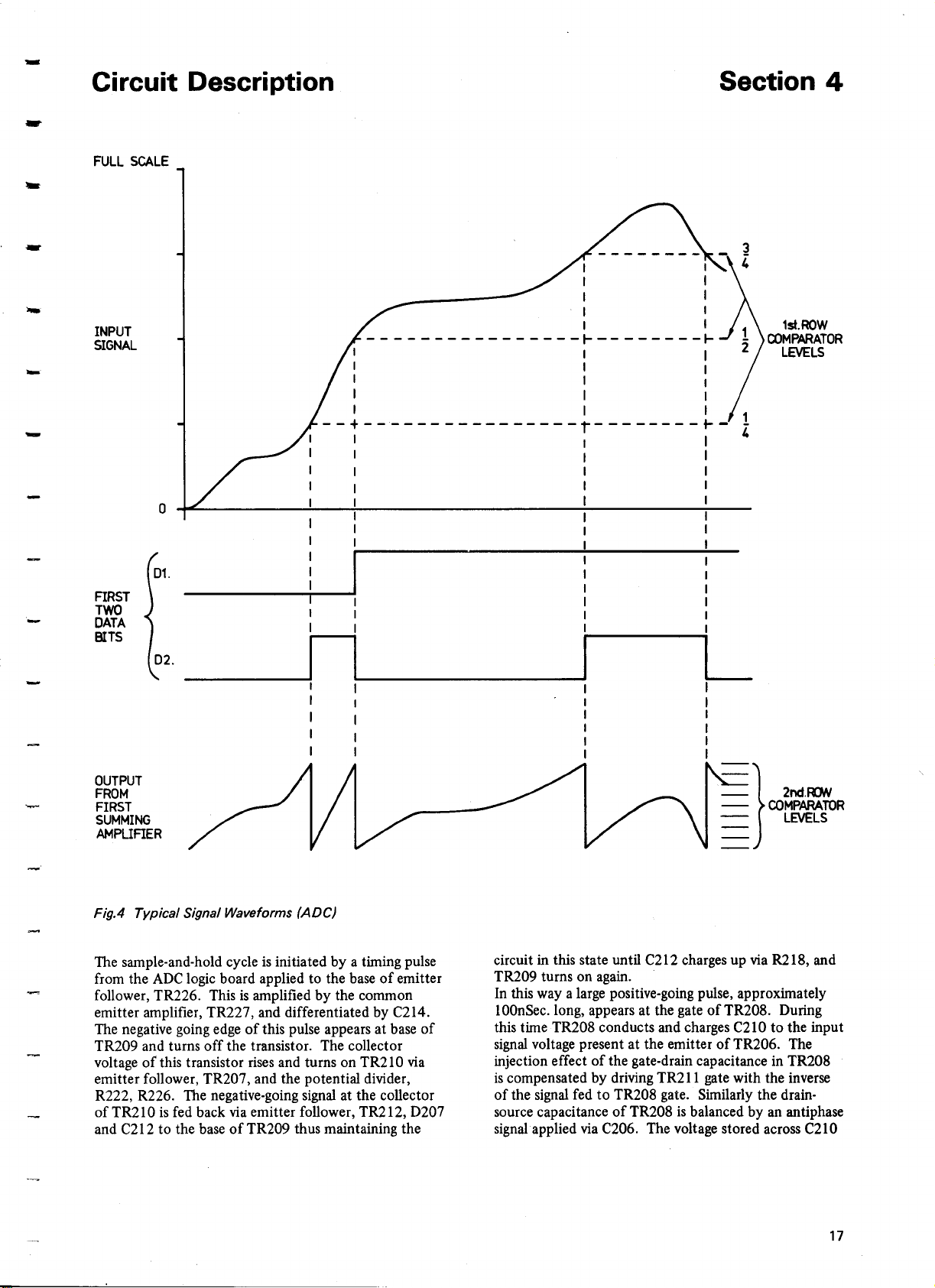
The timing signals for the system are derived from a
9.09MHz oscillator driving a divider which generates the
basic 5 phase I.82MHz clock. This circuitry is included
on the store logic board (see Fig.23). The waveforms
and relative timing are shown in Fig.5 and the method of
deriving them is explained in section 4.5.3. The five
subsidiary clock pulses are labelled PI to PS and these
are gated with the original clock frequency in various
combinations to derive the timing signals for the
decoding logic as shown.
The outputs of the first row of three comparators are
applied to the latching bistables, ICI20 a, b, c, which
are clocked approximately lOOnSec. after the end of the
sample-and-hold pulse to allow the comparators to settle.
Binary decoding is performed by ICI21 b, c and the de-
coded outputs applied to the first two switched current
sources which perform the function of the first DAC in
the block diagram Fig.4.3.I.
The outputs of the second row of comparators are
latched in two stages. The three outputs necessary to
obtain the two most significant of the three bits of data
available from this stage are latched in ICI23 a, band
ICI24 a. The outputs of these three latches are decoded
in a manner similar to the first row of comparators, by
IC122 c, d. The decoding of the third data bit is carried
out directly from the comparator outputs by ICI22 a, b,
ICI21 a, d and ICI25 a. The decoded output is then
latched by IC124b. To allow for the delay incurred by
these gates, the clocking pulse to IC 124 b is delayed with
respect to that applied to the other three latch bistables,
I
I
I I
IW
PiC;:
AT PIN 8 IC127
SAMPLE AND HOLD INITIATE PULSE
(LEADING EDGE)
LAST ROW LATCH PULSE
(LEADING EDGE)
Jl:
I I
I I
P30;PIN61C127
FIRST ROW LATCH PULSE
(TRAILING EDGE)
P4 PIN 1,e128
SECOND ROW LATCH PULse
(TRAILING EDGE)
I I
I I
I I
I I
I I
I I
n
by the four invertors, ICI28 a, b, e, f. The decoded
binary outputs are applied to the remaining three
switched current source circuits and remaining undecod-
ed fraction of the analogue input signal applied to the
final row of seven comparators. The decoding logic for
the final row is identical to that for the second row,
except that the least significant of the three decoded
bits is not latched at all hence there is no need for a
delayed clocking pulse to this section.
The relative timing of the various operations performed
during each cycle is shown in Fig.6.
4.4.5 CURRENT SOURCES
Within the A-D convertor circuit, Fig.22, there are a
total of eight current source circuits. Three are employed
supplying a fixed current to each of the resistor chains
which define the reference voltages for the comparators.
n
I
I
I
I
I
I
I
I
I
I
I
I
I
I
I
I
I
I
I
W
I
LLJ
I
I
I
r-
I
I
I
I
I
I
I
I
I
I
I
I
I
Page 18
Circuit Description
NOTE
ACTUALTIMES ARE SHOWN.
DETAILS OF S PHASE CLOCK
GENERATION ,PROPAGATION
TIMES ETC. NOT SHOWN.
t
LATCH PREVIOUS
DATA INTO STORE
CAl.CU.ATE
FIRST ROW COMPARATORS FIRST SUMMINGAMPLlFIE SAMPLE PERIOD
SECOND RDW COMPARATORS. SECOi'{) SUMMINGAMPLIFIER
SETTLE SETTLE
DS THIRD ROWCllMFr.RATms
LATCH LATCH DATA
D6.D7.D8 INTO STORE
+
The remaining five are switched by the data outputs from
the decoding logic. A common reference voltage is
supplied to all of the current source circuits by the
voltage regulator, ICIOl. The bases of the p.n.p. current
source transistors, TRl32, TRl36, TR139, TR141,
TR144, TR147, TRlS0 and TRlSl, are connected to
this reference line and precision resistors in the emitter
circuit define the collector current in each transistor.
The regulator, ICI0l, establishes the common reference
line by comparing the voltage across RI07, R266, R267
and R268 which is proportional to the output current of
the first current source, with its own internal stable
voltage reference. This internal reference, which is
available at pin 4 of ICI0l, is attenuated to a suitable
level by the potential divider chain, RI04, RI0S and
RI06, and applied to one input of the error amplifier,
pin 2. The other input of the error amplifier on pin 3
senses the voltage across the resistor chain mentioned.
In this way the regulator compensates for the effects of
supply line drift, temperature sensitive transistor
characteristics, etc. A current limit facility is provided
by the regulator: When the voltage drop across the series
resistor, RI03, exceeds one forward base emitter drop
(approximately 0.6 volt), the regulator is shut down
preventing overdissipation.
Two of the current sources, TRl32 and TR141, feed
buffer transistors, TRl33 and TR140, respectively, in
order to supply the relatively high currents required by
the first two comparator voltage reference chains.
The switched current sources are all identical with regard
to circuit operation. Taking TRl36 as an example, the
base of TR134 is driven by the most significant bit data
output at standard T.T.L. logic levels. A high level at
this point causes collector current to flow through the
load resistor, RIl3, and the catching diode, D101,
turning off TRl3S. The current source transistor,
TR136, then operates in the normal manner with it's
emitter current defined by R114 and RllS. A low level
at TR134 base turns off the transistor and R113 pulls
TRl3S base positive, turning this transistor fully on and
robbing TR136 of it's emitter current.
The currents of the first two switched current source
transistors, TRl36 and TR139, flow into a low impedance
mode in the first summing amplifier and the remaining
sources, TRI44, TR147 and TRlS0, into a similar point
in the second summing amplifier.
4.4.6
SUMMING AMPLIFIERS
The two summing amplifiers employed in Fig.22 are
identical except for the value of the feedback resistor
fitted. The component references mentioned in the
following description apply to the first amplifier which
drives the second row of comparators. ICI02 is an
integrated circuit array of five closely matched transis-
tors, two of these forming a long-tailed pair differential
input stage with a third acting as a current sink for this
stage. A p.n.p. common emitter stage, TR219, amplifies
the signal developed across the collector load resistors,
R237 and,R246, and an emitter follower, TR221,
provides a low output impedance. These stages form a
high bandwidth, differential input amplifier with
negative feedback applied via R249 to the inverting
input at the base of ICI02 b. The analogue input signal
from the sample-and-hold output transistor, TR21S, is
applied to the non-inverting input at the base of
ICI02 a, and appears at the output of the amplifier at
the emitter of TR221 by virtue of the unity voltage
gain feedback arrangement. However, the current from
the switched current sources is injected into the invert-
ing input of the amplifier at the base of ICI02 band
flows through the feedback resistor R249 developing a
negative offset voltage at the output, proportional to
the total current injected. Thus the output signal from
the amplifier represents the analogue input signal minus
the first two bits of data already detected, which
correspond to ~, h or ~ of the full scale input. The
signal fed to the second row of comparators and the
second summing amplifier input, ranges from zero to
one quarter full scale.
The second summing amplifier operates in an identical
manner except that the feedback resistor, R2S6, is one
quarter of the value of R249. This affects only the
magnitude of the injected currents which represent the
three bits of data detected by the second row of
comparators, that is
Y32to'1
full scale.
32
Page 19
Circuit Description
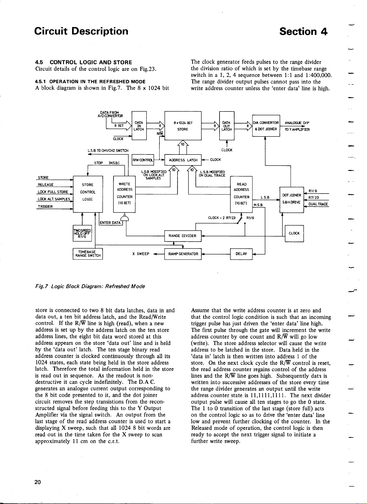
4.5 CONTROL LOGIC AND STORE
Circuit details of the control logic are on Fig.23.
4.5.1
OPERATION IN THE REFRESHED MODE
A block diagram is shown in Fig.7. The 8 x 1024 bit
STORE
RELEASE
LOCK FULL STORE
LOCK ALT. SAMPLES
TRIGGER
STORE
CONTROL
LOGIC
WRITE
ADDRESS
COUNTER
110 BIT]
The clock generator feeds pulses to the range divider
the division ratio of which is set by the time base range
switch in aI, 2, 4 sequence between 1: 1 and 1:400,000.
The range divider output pulses cannot pass into the
write address counter unless the 'enter data' line is high.
DIA CONVERTOR ANALOGl£ OIP
8
& DOT JOINER TOYAMPUFIER
READ
ADDRESS
COUNTER
110BlT]
M.s.B.
L.s.B.
DOT JOINER
S&H.DRIVE
R116
R7123
DUAL TRACE
store is connected to two 8 bit data latches, data in and
data out, a ten bit address latch, and the Read/Write
control. If the R/W line is high (read), when a new
address is set up by the address latch on the ten store
address lines, the eight bit data word stored at this
address appears on the store 'data out' line and is held
by the 'data out' latch. The ten stage binary read
address counter is clocked continuously through all its
1024 states, each state being held in the store address
latch. Therefore the total information held in the store
is read out in sequence. As the readout is non·
destructive it can cycle indefinitely. The D.A C.
generates an analogue current output corresponding to
the 8 bit code presented to it, and the dot joiner
circuit removes the step transistions from the recon·
structed signal before feeding this to the Y Output
Amplifier Via the signal switch. An output from the
last stage of the read address counter is used to start a
displaying X sweep, such that all 1024 8 bit words are
read out in the time taken for the X sweep to scan
approximately 11 cm on the c.r.t.
Assume that the write address counter is at zero and
that the control logic condition is such that an incoming
trigger pulse has just driven the 'enter data' line high.
The first pulse through the gate will increment the write
address counter by one count and R/W will go low
(write). The store address selector will cause the write
address to be latched in the store. Data held in the
'data in' latch is then written into address 1 of the
store. On the next clock cycle the R/W control is reset,
the read address counter regains control of the address
lines and the R/W line goes high. Subsequently dah is
written into successive addresses of the store every time
the range divider generates an output until the write
address counter state is 11,1111,1111. The next divider
output pulse will cause all ten stages to go the 0 state.
The 1 to 0 transition of the last stage (store full) acts
on the control logic so as to drive the 'enter data' line
low and prevent further clocking of the counter. In the
Released mode of operation, the control logic is then
ready to accept the next trigger signal to initiate a
further write sweep.
Page 20
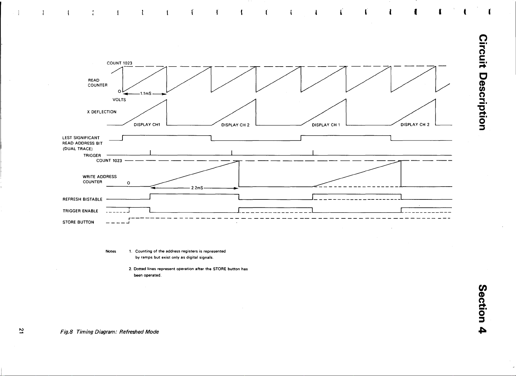
LEST SIGNIFICANT
READ ADDRESS BIT
(DUAL TRACE)
TRIGGER
COUNT 1023
WRITE ADDRESS
COUNTER
-----.J
0
Notes 1. Counting of the address registers is represented
by ramps but exist only as digital signals.
2. Dotted lines represent operation after the STORE button has
been operated.
Page 21
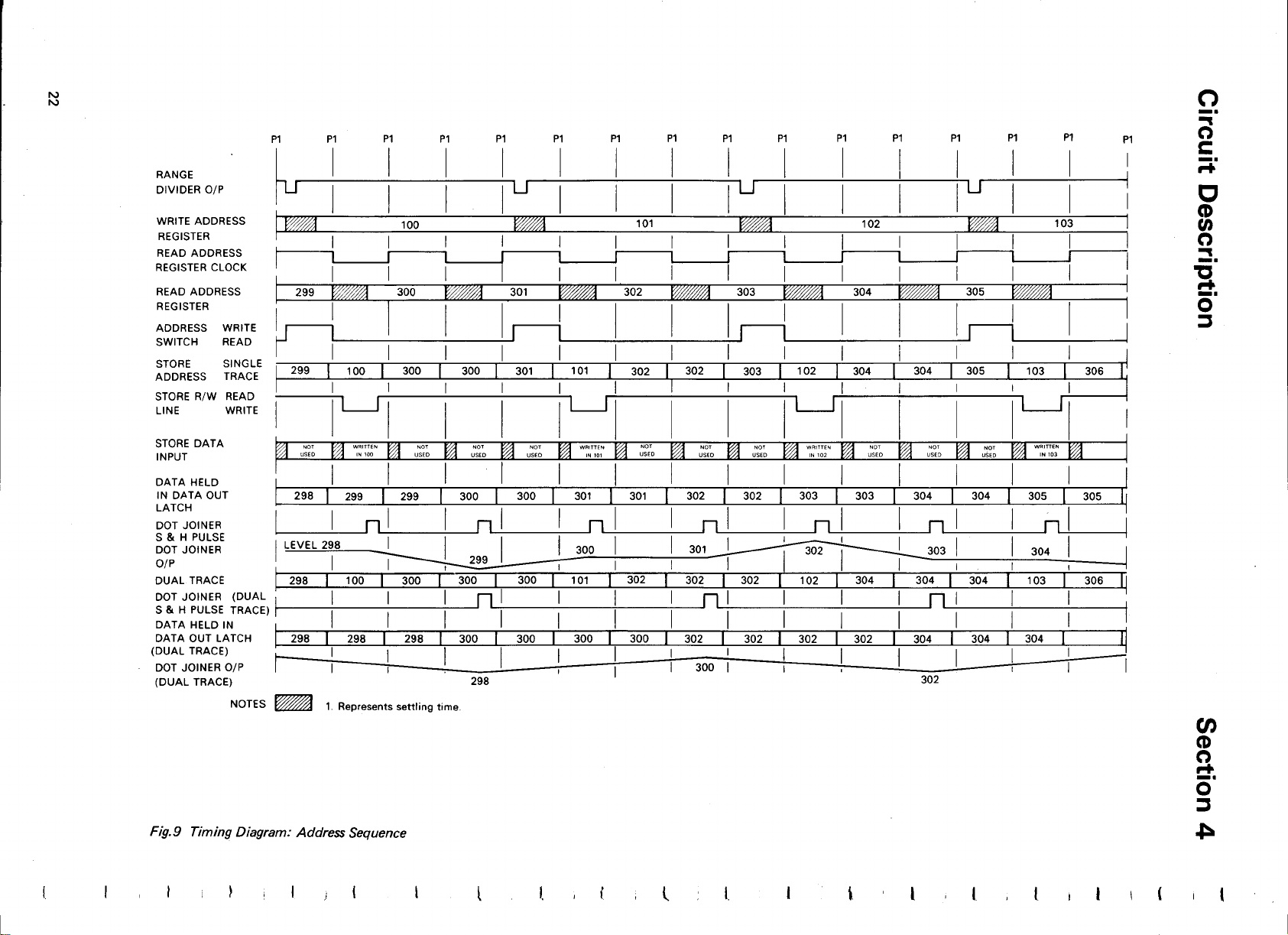
f'.)
f'.)
304
Pl
103
Pl
RANGE
DIVIDER
WRITE ADDRESS
REGISTER
READ ADDRESS
REGISTER CLOCK
READ ADDRESS
REGISTER
ADDRESS
SWITCH READ
STORE SINGLE
ADDRESS
STORE
LINE WRITE
STORE DATA
INPUT
DATA HELD
IN DATA OUT
LATCH
DOT JOINER
S&H PULSE
DOT JOINER
O/P
DUAL TRACE
DOT JOINER (DUAL
S&H PULSE TRACE)
DATA HELD IN
DATA OUT LATCH
(DUAL TRACE)
DOT JOINER
(DUAL TRACE)
RIW
O/P
WRITE
TRACE
READ
O/P
NOTES ~
Pl
~
Ifmt
I
299
I
~
I
Pl Pl Pl Pl Pl
I
I
u
I I
100
I
I
I
~
300
I
I I
I
1. Represents settling time.
I
I
I
EB
I
I
-
301
298
Pl
101
I
~
302
I
I I
n
300
Pl
Pl Pl
u
I
I I
I
W8
I
301
-
303
11
n
300
Pl Pl Pl
Pl
u
102
I
I
~
304
I
~
I
I
I
I
n
302
n
~
305
I~
I
I
I
I
~
I
n
-
.
••
n
c:
-.
r+
C
m
tn
n
_.
••
"tS
r+
_.
0
~
en
m
n
r+
-.
0
~
Fig.9 Timing Diagram: Address Sequence
~
l
I.
I
Page 22

Circuit Description
Section 4
If the STORE button is pressed, the control logic is
locked at the next 'store full' signal and the effect of
further trigger pulses is inhibited. If the STORE button
is again pressed the control logic allows one single
triggered write sweep but if the RELEASE button is
pressed, the trigger inhibition is removed completely.
Typical operation is shown in Fig.8 for the 200J1s/cm
range. The increasing count in the address counters is
represented as a ramp. The read/write interlace applies
for time base ranges lOOJ1s/cm to 20s/cm. Alternate
clock pulses are used for read, leaving the rem aining
alternate periods available for write entry if called for
by the range divider. Fig.9 shows this sequence for
range 8.(200J1s/cm). The initial addresses for this
diagram are chosen at random but the subsequent
sequence is relevant.
On range 6 and faster, the maximum writing speed of
the store is used
(550J1s
per address), and the control
of the store address lines is passed to the write address
counter for the time required to enter the 1024 new
data words. The read system then holds-off trigger
pulses until two reading sweeps have taken place.
4.5.2
OPERATION INTHE ROLL MODE
A block diagram of the system in the Roll mode is
shown in Fig.lO. The read and write counters are
clocked as for the refreshed mode, and the 'data in'
latch, store, data and latch, and address selectors
function in exactly the same way as for the Refreshed
mode. The essential differences are:
a) The display sweep is started from parity between
the read and write address rather than from zero
read address. This gives the effect of a moving
display.
b) Data is entered continuously and trigger pulses
have no effect until operation of the STORE
button enables a trigger pulse to initiate a STOP
sequence.
To generate the concidence signal which initiates the
display sweep, the 10 address lines of the write and
read address counters are connected to an eight bit and
two bit comparator whose outputs are taken to a two
input NAND gate. When the same address is present
on the counters the gate output goes low and after a
short delay the display ramp is started. As can be seen
STORE
RELEASE
LOCK FULL STORE
LOCK ALT. SAMPLES
TRIGGER
STORE
CONTROL
LOGIC
DIA CONVERTOR ANALOGUE 01 P
&
DOT JOINER TO Y AMPLIFIER
CLOCK
PULSE
ADDER
IR116 I
Page 23

Circuit Description
READ
&
WRITE ADDRESS
COUNTERS
Notes 1/ Operation shown for trigger position switch set tol(full scan
2/ Countofread and write address is shown as a ramp
but exists as a digital signal
from Fig.1l, the write address counter is stepped-on at
a slow rate determined by the range divider while the
read address counter is stepped at a fixed fast rate.
The comparator output occurs at the address where
new information is being written into the store, and
the displaying sweep started at this point (after a short
delay) will display the oldest information first (left
hand side of display) and the newest last (R.H.S.)
When the Roll mode is selected while released, the
store control logic drives the 'enter data' line high,
trigger pulses have no effect on the operation of the
system and the display follows the incoming data.
If the STORE button is now pressed, the store control
logic can accept a trigger signal and the address present
in the write address counter at the instant of trigger, is
held in the ten bit Trigger Point Store latch. The eight
least significant bits in the latch are compared with the
eight least significant bits of the write address counter.
The two most significant bits held in the latch are
added in a 2 bit binary adder to a two bit number set
up by the Stored Trigger Point switch, before being
passed to a two bit comparator to be compared with
the most significant two bits of the write address
counter.
If the number set up by the switch is 00 the comparator
gives an output immediately after Trigger, which acting
on the store control logic, drives the enter data line low,
stopping any further information being written into the
store. If the number set up by the switch is 01 (Y<!full
count), 10 (lh full count) or 11(%full count), the write
address counter must count on this amount before the
comparator will generate an output and stop the entry
of information. As the write address counter is now
stable, every display sweep will be started at the same
store address, and therefore the displayed waveform
will be stationary.
4.5.3 CLOCK GENERATOR
The clock oscillator consists of TR602- TR603 connect·
ed as an emitter coupled oscillator, C60l being adjusted
to set the frequency to 9.09MHz. TR601 is a buffer
enabling the oscillator to drive the clock lines of the
two dual bistables, IC's 610, 602. These are connected
as a four stage shift register, but with the first input
(pin 2, IC 610) controlled from the output of a four
input NAND gate, IC603 b, whose inputs are connected
to all four bistables. Therefore the input to the shift
register cannot go high until allQoutputs are low, and
will go and remain low while a single high state is
propagated down the shift register. The outputs from
the bistables are inverted by IC61l, and called PI, 2,
3, 4. P5 is taken directly from pin 8 IC603. The width
of a P pulse is liOns and the period is 550ns.
4.5.4 READ AND WRITE COUNTERS
The write counter consists of two four bit binary
counter integrated circuits, IC655, 647 and a dual J.K.
bistable package, IC639, connected as a two bit divider.
Outputs are labelled Bl (least significant bit) to B10
(inost significant bit) on the circuit diagram.
The read address counter consists of two four bit binary
dividers, IC's 656, 648, and the dual bistable, IC640,
connected as a two bit binary divider. The clock pulse
for this counter comes from IC707c, which together
with IC707d, a, and IC720b select the PI pulse on
ranges 50/.1s/cm and above, or the output from the first
stage of the range divider on the lower ranges. The
least significant bit of this counter (Cl) is applied to
the selector, IC7l9, whose output (C I') is connected to
the store address selector. If a single trace mode is
chosen the DUAL TRACE line operating on IC7l9
allows Cl to pass to the output. In the dual trace
mode, Cl is blocked and the output of gate, IC719a,
is determined by bistable, IC723a. This bistable is
clocked by the display ramp bistable, such that on
alternate sweeps odd and even read addresses are
selected.
4.5.5 STORE. INPUT. OUTPUT AND ADDRESS LATCHES
The timing diagram Fig.9 includes details of the events
in the 1.1/.1speriod taken by a write and read cycle in
the store. First, the ten address lines for the store must
Page 24

Circuit Description
Section 4
be set and held at a new number, then new input data
is set and held on the 'data in' lines. To write in data
at this address the RjWline is taken low after lIOns for
330ns. True 'data out' is available 500ns after a new
read address in set up.
The 'data in' latches consist of IC's 618, 619,
which are clocked by the PI. The address latches
(IC's 652, 644, 636) are controlled by a pulse which is
positive-going during the last half of the PS period.
If a write cycle is to take place (Q of IC620a is high)
the store R/W line is taken low from the beginning of
P2 to the end of P4 period by the P2 and PS pulses
acting on the bistable formed by IC625 c, d. Output
data appearing on pin 12 of the R.A.M.'s is held in the
8 bit 'data out' latch consisting of IC650, 659, by the
leading edge of a positive-going pulse which is the
address latch pulse inv:erted by IC625.
4.5.6
COMPARATORS
Three comparators are required. These are for 'stop on
roll', 'trigger point bright-up' and 'display ramp start'.
The circuits used are all quad exclusive NOR two input
gates (8242 or equiv.) with open collector outputs. By
connecting outputs together, two n bit binary numbers
may be compared, and when they are equal the output
will go high. These comparators function only in the
roll mode.
The 'display ramp start' pulse is generated by exclusive
NOR gates, IC654 a, b, c, d, IC646 a, b, c, d, which
compare the eight least significant bits of the read and
write counter, R618 is the common load resistor and
IC638 c, d, compares the two most significant read and
write address bits, with R617 as the load. The two
outputs are then applied to two inputs of the 3 input
NAND gate, IC632C, together with the P4 pulse which
acts as a strobe, allowing the state of the read and write
counter to settle before the result of the comparison
can pass to the output of IC632C.
The 'stop on roll' output is generated either immediately
on receipt of trigger or after the write address counter
has counted another quarter, half or three quarters of
its full count. This is controlled by the front panel
lever switch STORED TRIGGER PT. S602. When a
trigger signal is received, the PS pulse immediately
following the trigger signal is gated by IC605d, and acts
as a clock pulse on the ten bit latch, IC613, 621, 629,
the inputs of which are connected to the write address
counter. Therefore the write address set up at the
instant of trigger is held in this latch.
The eight least significant bits held in the latch (outputs
IC613, 621) are compared with the eight least significant
write address bits, by 1C614, a, b, c, d, IC622, a, b, c, d,
whose common load is R627. The two most significant
bits stored in the latch are applied to the two bit binary
full adder, IC631, together with a two bit binary number
derived from the front panel switch, S602. The result
of this addition is applied to the comparators, IC623, a,
b, and compared with the two most significant bits of
the write address register. IC623d which compares the
PI pulse with OV is also connected to the common out-
put load R627. If the number set up by S602 is 00
there will be an immediate equality between the write
address number and the latch number, so that during PI
period the comparator output will go high. If S601 sets
up 01 so that the number held in the latch is increased
by one quarter of the full count before being applied to
the comparators, the write address counter will have to
count on for a quarter of its full count to generate an
output. Similarly the output is delayed by half or three
quarters full count for the other positions of S602.
The number set up by S602 can be reduced to zero by
gates IC606, b, c, when their inputs are driven high.
This is done during the trigger enable sequence described
in section 4.6.3.
To generate the 'trigger point bright-up' the read
counter is compared with the number held in the
trigger point store. The eight least significant bits are
already compared in IC654, a, b, c, d, and IC646, a, b,
c, d. The two most significant bits are compared by
IC638, a, b, with R619 as the common load. The out-
put of IC654, 646, and the output of IC638, a, b, are
taken to two inputs of a three input NAND gate,
IC632b, the third input of which goes high when both
inputs of IC630a are high. The trigger point is only
marked when the roll mode is selected and the STORE
1.e.d. is illuminated.
4.5.7
RANGE DIVIDER
The divider consists of a multi-decade divider package,
IC711 (Mostek 5009), and a dual distable, IC722,
connected as a .;-2 .;-4 stage. PI and P4 pulses applied to
the cross-connected gates IC728 a, b, cause the output
of 728a to "gohigh from the beginning of PI to the
beginning of P4. The output of 728b is complementary.
Output 728a is used to clock 722a, a J.K. bistable with
J.
and K. high, changing its output on the negative going
edge. TheQoutput of 722a is used to clock 722b where
1. and K. input are also high. Therefore the Q output of
722a is a square wave of half the P pulse frequency
(0.909MHz) and the Q output of 722b is a square wave
of one quarter the P pulse frequency (0.455MHz). The
outputs from 728b, 722a, 722b, are applied to the
selector, IC717c, IC706a, b, c, which is driven from the
timebase range switch via the inverters, IC705d, e, f.
The state of the three control lines, 9L, 12L, 15L, for all
ranges is shown in the following table. For el'ample when
the timebase switch shorts 9L to ground, output 705d
goes high enabling the output from 722a (0.909MHz) to
pass to IC717. Only one line out of three is shorted on
any range, the other two being high. In this particular
case, outputs 705f, e, will be low and will drive the out-
put of 706b, c, high. Therefore only the 0.909MHz
signal will appear at outpufIC717c. This output is used to
clock the decade divider, IC711. This is an M.O.S.
device and requires a -12V line which is derived from
the -20V line via R795 and D711. The division ratio of
this IC is set by the three lines controlled by the time-
base switch, (16L, lOL, 6L) as shown in table overleaf.
Page 25

Circuit Description
Section 4
Range Divi er
1/lS/cm
2lls/cm
5/lS/cm
lOlls/cm
20lls/cm
5Olls/cm
1001ls/cm
2001ls/cm 8
500/lS/cm 9 10 1
Ims/cm 10
2ms/cm 11 40 1
5ms/cm 12 100
lOms/cm
20ms/cm 14 400
50ms/cm 15 1000
lOOms/cm 16
200ms/cm 17 4000 1 1
500ms/cm
Is/cm
2s/cm 20
5s/cm 21 100,000 1
lOs/cm 22 200,000
20s/cm 23 400,000 1
Range
No.
2 1
3 1
4
6
7
13
18 10,000
19 20,000
Rand':
Ratio
1 1 0 0 0 0 1 1
5 1 0
4
20 1 0 0 1
200
2000 1 1 0 1 0 1
40,000
RangeDivider Control Lines
L16 L10 L6 L15 L9 L12
0 0 0 0
0
0
1 0
1 0 0 0 0 1 1
2 0 0 0 1 0 1
0 0 0 1 1 0
0
0
0 1 0 1 1
1 1 0 0 1 1
0
0 0 1 1 0 1
0 0 1 1 1 0
1 0 1 1 0 1
0 0
0
0
0 0 0
0 0 0
0 0
1
0 0 1 1
1
0
0
1
0
1
0
1
0
1 1
1 1
1 1
0
1 1
1 1
0
1
1 0
1
0 1
I
1
1 1
0
1 1
0
1 1 0
1
0
0
The output from the decade divider is taken via the buffer-
ing inverters, IC705, a, b, to the clock input of the
bistable, IC718a. The output of the range divider takes
various positions relative to the system clock depending
on the division ratio selected. IC718, a, b, is used to re-
clock the divider output pulse at
n.
The decade divider
output makes IC718a Q go high, driving high the J.and K.
inputs of IC718b. The next P2 pulse allowed through the
gate IC706d, will set Q IC718b high, Q IC718b low thus
clearing IC718a. IC718b is cleared by the P3 clock pulse.
Therefore IC718b Q is high for the P2 time after an out-
put pulse from the range divider. These pulses are applied
through gate, IC732c to the write address counter.
4.5.8 DISPLAY RAMP START AND STOP
Ramp Start Selection
The ramp start pulse is generated either by the most
significant read address bit (Refreshed Mode) or by the
ramp start comparators, IC654, 646, 638 acting on IC632c
(Roll Mode). One of these two signals is selected by the
selector, IC740, a, b, c, d, and appears at the output of
IC740d. Selection is controlled by IC728c and IC717a.
In the refreshed mode the ROLL line is low, driving the
output of IC728 high and passing the most significant
read address bit through the gate, IC740. The other input
to IC728 controlled by IC71 7, can have no effect. In the
Roll mode, for the output of IC728c to go low and select
the signal from the ramp start comparators, the output of
IC717a must also be high. It can be seen from the input
connections of IC717a that on the fastest ranges (1/7) if
the STORE 1.e.d. is not lit and the 100% HOLD button
not pre'ssed, the output of IC717a will be low, forcing
IC728c output high, resulting in the ramp start being
derived from the read counter. This is necessary since on
the fastest ranges the read and write counters are being
clocked at the same frequency and therefore would never
become coincident. When the STORE 1.e.d. is lit or the
Lock Full Store button pressed, the write address counter
is not counting and coincidence pulses will again occur and
can be used to start the displaying ramp.
Ramp Start Delay
The selected output is used as the clock input to the mono-
stable pulse generator circuit consisting of a J.K. flip flop,
IC741a, TR715, R771/772 and C718. In the quiescent
state, Q of IC741a is low, TR715 is off and its collector
load, R772, pulls the 'clear' input ofIC741 a high.
Conditions around IC741a are:- Clear and 'preset'are
high, J is high and K is low. A negative transistion on the
clock input will cause the Q output to go high and the
Q
output to go low. This negative step is transmitted via
C718 to the base of TR715, driving it negative by about
3V w.r.t. ground, but the current through R771 charges
C718 eventually pulling the base ofTR715 above ground
potential and turning on TR715. The delay time is there-
fore set by R771 and C718. The collector ofTR715 goes
low, applying a 'clear' input to IC714a to drive Q high and
Q low. C718 is rapidly charged via the base-emitter
junction ofTR715, but as the charging current falls to
zero, TR715 again turns off, thus returning the circuit to
its original condition.
Monostable, IC741a, does not perform a delaying function.
In the ROLL mode, because the result of the comparison
between read and write counters is strobed by P4 to allow
for settling times, but the read counter is being clocked
on most ranges at one half the clock frequency, the ramp
start output consists of a pair of pulses. The delay set by
IC741a is sufficient to ensure that the second pulse of the
pair is ignored.
The negative transistion at Q IC741 a caused by the first
ramp start pulse, is used as the clock input to an identical
circuit, IC739a, TR717, R794, R793, C714, which gener-
ates a pulse width of approximately 2/1s.
Ramp Stop
The Q output of IC739a acting through IC717b and
IC728d turns on TR718 for this period, driving the 'clear'
input of the display ramp bistable on the timebase p.c.b.
(IC903b) low, thus ending the displaying ramp if it is
running at that time.
Ramp Start
The negative transition at Q-IC739a when it returns to
the quiescent state, clocks IC739b, a J.K. flip flop
connected as a divide by two. Assume that the clock
pulse drives Q-IC739b from low to high. The 'clear'
inputs to IC741b and IC742b are now removed and
IC742b can respond to pulses on its clock input. These
are the gated P4 pulses used as sample-and-hold pulses
for the dot joiner circuit, and can be at full clock rate,
half clock rate or quarter clock rate depending on time-
base range and single/dual trace operation. The first P4
pulse incident on the clock input of IC742b after the
clear input has been removed, will drive Q-742b high,
and the second will drive Q-742b low, Q-742 high
Q-741b lbW, which makes the J & K inputs ofIC742b
Page 26

Circuit Description
Section 4
both low, preventing further clock pulses having any
effect. The low/high transition ofQ-IC742b acts as the
ramp start pulse through connection N/MI6 and gate,
lC904d, on the clock input of the ramp start bistable,
IC903b.
The next ramp start pulse from the read counter or
comparator system will, via monostable, IC741a, drive
IC739a to the opposite state, Le. Q high to low. Thus
Q-IC741b is returned to the high state, Q-IC742b is
held in its high state and cannot generate a ramp start
signal. Therefore the ramp start signals are divided by
two, but the ramp stop signals are not. The generated
sequence of signals is:- STOP START - STOP - STOP
START - STOP - STOP START, etc. The STOP
signal immediately prior to the START signal has no
effect as the displaying ramp is not running at that time.
Read Counter Clock Pulse Adder
On ranges 1/6 in the Roll mode before the STORED
condition is reached, the write address counter is in
control of the store address lines and the read address
counter does not determine the address of the information
read out into the 'data out' latch. The information held in
this latch is that which has just been written into the store.
If the front panel controls have been set to call for dual
trace operation (CHI and CH2 operation or LOCK ALT.
SAMPLES) the dot joining circuit will receive a sample-
and-hold pulse at one half the clock rate (the least signifi-
cant bit of the read address counter acts on gates, IC725a,
b, and IC732a, to allow only every other P4 pulse through
to drive the dot joiner sample-and-hold cct). To prevent
this pulse from sampling the information in the same set
of alternate addresses on every displaying sweep, an extra
clock pulse is inserted into the read address counter input
after every other full count. This ensures that the sample-
and-hold pulse samples even address information on one
displaying sweep, and odd address information on the
next sweep and so on. This extra pulse is generated by
IC72I, and IC720.
Bistable, IC72I a, is connected as a binary divider, with
the clock input taken from the most significant read
address bit. On every other full count output from the
read address counter, Q-IC72Ia goes low clocking the
binary divider, IC72Ib, driving its Q output high, and
allowing the next P3 pulse via IC720a to pass gates,
IC720c, IC720b and IC707c, to appear as a clock pulse
at the input of the read address counter. The following
P5 pulse acts on the 'clear' input of IC72I b to return its
Q output to ground and close gate, IC720c.
4.6
MODE CONTROL
4.6.1
DISPLAY MODE LOGIC
The switch, S60I, has three positions, Normal, Refreshed
and Roll. When the timebase range switch is set between
the 500ms/cm and the
IJ.1s/cm
range the pole ofSIOIa is
connected to ground via S6, so that in the up position the
l.e.d. indicating normal operation, D60I, is lit, the centre
position illuminates D602 (Refresh indicator) and the
bottom position illuminates the roll indicator, D603.
When the timebase is set between ranges Is/cm to 20s/cm
the pole of S60Ib is grounded so that in the up position,
D602 is illuminated indicating that the refreshed mode is
operating. Outputs from this switch to the control logic
are on 7H (NORM) and 5H (ROLL).
One of the l.e.d.'s, D601, 602, 603, is always lit unless the
STORE l.e.d., D7I7, is on, in which case the base drive to
the p.n.p. transistor, TR70I, is removed and no current
can flow through R609 to these l.e.d. 's.
4.6.2
HOLD
Output pulses from the range divider must pass through
the three input gate, IC732c, to the input of the write
address counter. The Lock Full Store push button, S703a,
drives a slave bistable, IC702a, d, for switch de-bouncing.
When the button is pressed the input of invertor, IC727d,
goes high, putting a low on one input of IC732c, cutting
off this gate.
The LOCK ALT. SAMPLES button, S704a, driving a similar
bistable, IC70Ia and d, puts alow on IC707c, blocking the
signal from the least significant write address bit (B 1) and
driving the least significant write address line (Bl) per-
manently high. Half the contents of the store cannot now
be addressed by the write counter, but will continue to be
displayed. Action of the dot joiner requires that if single
channel operation is in progress, two display traces must
be established, one the held information and the other the
current information.
IC70Ia and d, drives high both inputs of the open collec-
tor gates IC735, so that the DUAL TRACE line is pulled
low. This causes the least significant bit of the read
address to come under the control of the display ramp
bistable su~h that alternate sweeps display odd and even
store locations as for any dual trace display.
4.6.3
STORE AND RELEASE
Fig.I2 shows a simplified section of this part of the
complete circuit of Fig.23.
Operation in the Refreshed Mode
Assume that the RELEASE button has been pressed.
Bistable, IC708a and IC726a, are cleared, Q-IC726a is
high so that the ARMED l.e.d., D7I6, is off, and
Q-IC708a is low applying a low input to the two gates,
IC733a and IC732b, driving their outputs high, so that
the TRIGGERED and STORED l.e.d.'s are off. The
output of IC732b (high) drives on TR70I via IC702b
so that l.e.d., D602, controlled by the mode switch,
S60I, is lit. The gate, IC73I c, has two high inputs,
Q-IC708a and the ROLL line, so that its output is low.
This turns off IC713b so that its output will rise if the
"wired or" gate, IC7I3c, is also off. This gate is con-
trolled by the two sweep hold off system, IC723a, b
(described later) and may be assumed to be off in this
section. Consequently the trigger enable line is always
high after the RELEASE button has been pressed.
When the STORE Qutton is pressed bistable, IC726a, is
clocked such that Q goes low turning on the ARMED
l.e.d. Gate, IC73I b, now has two high inputs, Q-IC726a
and Q-IC726b (thiS bistable is held preset by the ROLL
Page 27

Circuit Description
STORE
1
RELEASE ~
57020
line being low), and so its output is low. This, acting on
IC713b, holds its output high as before. The action of
pressing the STORE button also clocks bistable, IC708a,
such that theQgoes low driving high the other input to
IC713b via IC713b. The result is that the trigger enable
line is still high but this is now conditional on the state
of the trigger enable bistable, IC726a. The gate controll-
ing the TRIGGERED l.e.d. now has one high input (Q-
IC708a) and one low input (Refresh B/S-Q) so that this
l.e.d. is still off. The gate controlling the STORED l.e.d.
has two high inputs (Refresh B/S-Q and Q-IC708a) and
one low input (Q-IC726a) so this l.e.d. is also off.
When a trigger signal occurs, the refresh B/S-Q goes high
and this operating through invertor, IC727a, on the 'clear'
input of IC726a, resets it, turning off the ARMED l.e.d.,
D716. The gate controlling D718 now has two high in-
puts so this l.e.d. (TRIGGERED) is lit. The gate control-
ling the STORE l.e.d., IC732b, now has two high inputs
(Q-IC708a and Q-IC726a) and one low input (Q-
Refresh B/S), so the l.e.d. is off.
On completion of a writing sequence the RefreshQ output
will go low, turning off D718 and turning on D71 7, the
STORED l.e.d. It also turns offTR701 and extinguishes
the Refreshed Mode indicator l.e.d. D602. Q of IC726a
going low, drives the trigger enable line low via the two
invertors, IC73lb and IC713b.
Pushing the STORE button again will clock Q-IC726a to
the high state, so driving the trigger enable line high until
another trigger signal is accepted. Pushing the release
button sets Q-IC708a high, driving the trigger enable line
permanently high via gates, IC731b and IC713b.
Two Sweep Hold-Off Circuit
This circuit only operates in the refreshed mode on the
timebase ranges 50lJ.s/cm to IlJ.s/cm.
On these timebase ranges it is necessary that the writing
sequence interrupts the reading sequence (this is described
in section 4.5.1). If the system were allowed to respond
to rapid trigger pulses, no full reading of the store would
occur resulting in a blanked display. To prevent this,
after every writing sequence the trigger enable line is held
low until two reading sweeps have taken place.
Under all other conditions the line, TOP6 REF, will be
low, presetting bistable, IC723b, and applying a perman-
ent low to IC713c turning off this half of the "wired or"
gate, so that the state of the trigger enable line is control-
led only by IC713b.
When the TOP6 REF line is high, the preset input is
removed from IC723b. When the refresh B/S-Q is set
high by a trigger signal at the start of a writing sequence,
the ,output of gate, IC729c, will now go low setting the
Q output of IC723b high and the Q output of IC723a
high. IC713c is now turned on and the trigger enable line
pulled low. The display ramp B/S-Q will go low on the
completion of the current reading sweep, but this cannot
clock IC723a because of its preset input.
No more display ramp sweeps take place until the end of
the writing sequence. When the refreshed Q goes low,
displaying sweeps can again occur. The output of IC723a
will change at the end of every display sweep (this output
is used to generate the l.s.b. of the read address when dual
trace operation is called for), and after two sweeps, the 0
output of IC72~ going negative acts as a clock pulse on
IC723b setting Q low and therefore making the trigger
enable line high by turning off IC713c.
Operation In The Roll Mode
Operation of the ARMED, TRIGGER, and stored l.e.d.'s
is the same as for the refreshed mode previously described.
The action of the trigger enable is as follows:-
Assume the RELEASE button has been pressed so that
Q-IC708a is high, Q-IC726a is low, and also that the
output of the roll hold-off circuit, Q-IC726b, is high
(this is described later). The ROLL line being low drives
high the output of gate, IC731c, and Q ofIC726a acting
through inverter, IC731b, also applies a high input to
IC713b, turning on this gate and driving low the trigger
enable line. As the STORE l.e.d. is off, IC733c has two
high inputs thereby applying a low input to the 'enter
data' gate, IC733b, forcing its output high so that data is
written into the store continuously. Trigger signals will
have no effect until the STORE button is pressed. This
sets Q- IC726a high, and via the two inverters, IC731 b
and IC713b, sets the trigger enable line high. The
ARMED l.e.d. is also illuminated. When a trigger signal
sets the refreshed B/S-Q high bistable, IC726a, is reset
Page 28
Circuit Description
Section 4
by inverter, IC727a, turning off the ARMED l.e.d. and
returning the trigger enable line to the low state. The
TRIGGERED l.e.d. is illuminated as previously described
until a STOP signal from the store sets the refreshed
B/S-Q low. This causes the TRIGGERED l.e.d. to be
extinguished and the STORE l.e.d. to be lit. IC733c now
has one low input, driving its output high, and the 'enter
data' gate, IC733b, has two high inputs making its output
(the ENTER DA TA line) low. Loading of the store is
therefore prevented, until either the RELEASE button or
the STORE button is pressed. If the RELEASE button is
pressed, IC708a is cleared driving one input of gate,
IC732b, low and so turning off the STORE l.e.d. Gate,
IC733c, now again has two high inputs, and its output
acting on IC733b drives high the ENTER QATA line.
If the STORE button is pressed, IC726a-Q is set low
driving low an input to IC732b, extinguishing the STORE
l.e.d. and causing the ENTER DATA line to go high.
Roll Hold-Off
When the sequence ARMED, TRIGGERED, STORED, has
occurred the STORE LED line acting on the 'clear' input
ofbistable, IC742a, sets its Q low, applying a 'clear' to
bistable, IC726b, setting its Q output low. This, acting
through inverters, IC73 I band IC713 b, ensures that the
TRIG. ENABLE line is held low when the STORE button
is again pressed. Data will be loaded but the refresh B/S
will not respond to trigger signals. The bistables, IC726b
and 742a, provides hold-off such that when a trigger is
eventually accepted and the store generates a STOP signal,
the final display consists entirely of information loaded
after the last pressing of the STORE button. Without this
hold-off, a trigger signal could be accepted immediately
and if the stored trigger point switch was set to its top
position (100% pre-trigger), the display would consist
almost c;;ompletely of old (previously stored) information.
When the STORE button is pressed, the write address
counter is clocked and the least significant write address
bit (Bl) is used to clock IC742a, setting Q high, and
this applies a high to theJinput of IC726b, and also
removes the low on its 'clear' input. This bistable can
now respond to the store STOP output acting on its clock
input. This will be generated by the next equality to
occur between the number generated by the write address
counter and the number held in the trigger print store.
(This isnot modified by the two bit adder circuit since the
number set up on the stored trigger point switch, S602, is
made 00 by the gates, IC606c, d, turning on when the
refreshedClline is high.) The clocking of IC742a by B1
ensures that IC726b is not cleared immediately by an
existing equality between the write address counter and
the trigger point store (S602 previous set to END TRACE
position). When the STOP signal occurs, Q-IC726b, is
set high enabling gate, IC731 b, and allowing the TRIGGER
ENABLE line to go high.
4.6.4
NORMAL MODE BEAM SWITCHING AND CHOP
BLANKING
When S601 is set to normal, the read and write counters
and the store continue to operate but their precise
functioning in this mode is not important. Normal
oscilloscope operation will be maintained as long as the
timebase switch is set to range 18 or faster. Selecting a
range below this will automatically bring in the refreshed
mode.
In the normal mode the logic must provide several
functions:-
1. Beam switching pulses ('Chop' and 'alternate' depend-
ing on timebase range).
2. Chop blariking pulses.
3. Trigger enable.
4. Connect the composite signal from Y input to Y out-
put stage.
The inputs of the quad open collector NAND gate, IC71O,
are driven from the range switch and the mode switch to
provide in normal operation, two lines which are used to
obtain the required function.
a) A high on ranges 12/23 + normal line (BOT. 12 NORM).
b) Its inverse (O/P IC7IOd).
A "low on norm" line is obtained from S601. The time-
base range switch connects 8L to ground on ranges 17/1
and hence S601 will ground cathode ofl.e.d., D607, the
anode of which is fed via the saturated transistor, TR701,
from the +5V supply. D601 is therefore lit, indicating
normal operation.
Beam Switching
CHI, CH2, or dual trace operation is selected by S603
acting on gates, IC736c and d. When input 10 of IC736c
is set low, its output is set high, selecting CH2. When in-
put 12 of IC736d is set low, output IC736c is set low,
selecting CHI. Ifneither 10, or 12 ofIC736 is set low,
control of-channel selection is passed to 13 of IC736d,
which is connected to the output of the signal switch,
IC709a, b, c, and d. In the normal mode, the "NORM"
line acting on 9, 10 and 4 of IC709, prevents the signal
from the write address counter (12 oflC655) from
passing through, and enables the signal from Q of IC708b
to control the beam selection. This bistable is switched
in two ways depending on the range setting, low sweep
speeds select CHOP, high sweep speeds select ALTER-
NATE.
On ranges 12/17, the BOT. 12. NORM.line acting on the
'clear' input of IC708b drives Q low, Q high. However
the 'preset' input is driven from the gate, IC729a. As 2
oflC729a ishigh (BOT. 12. NORM line), the signal on
the output of IC729a which is obtained from the second
stage of the read counter, will control the state of the
'preset' input of IC708b. When the 'clear' is low and
'preset' high, Q is low,Qhigh. When 'clear' is low and
'preset' is low,Clis high andClis high. Therefore,
although the bistable does not change from one stable
state to the other, the output at Q changes under the
control of the second stage of the read counter. On the
ranges 12/18 therefore the beam switch is operated at a
frequency of 227kHz (chop mode). On ranges 11/1 the
BOT. 12. NORM line drives the 'clear' high, and its
inverse, acting through gate, IC729a drives high the
'preset' of bistable, IC708b. Therefore this bistable is
Page 29
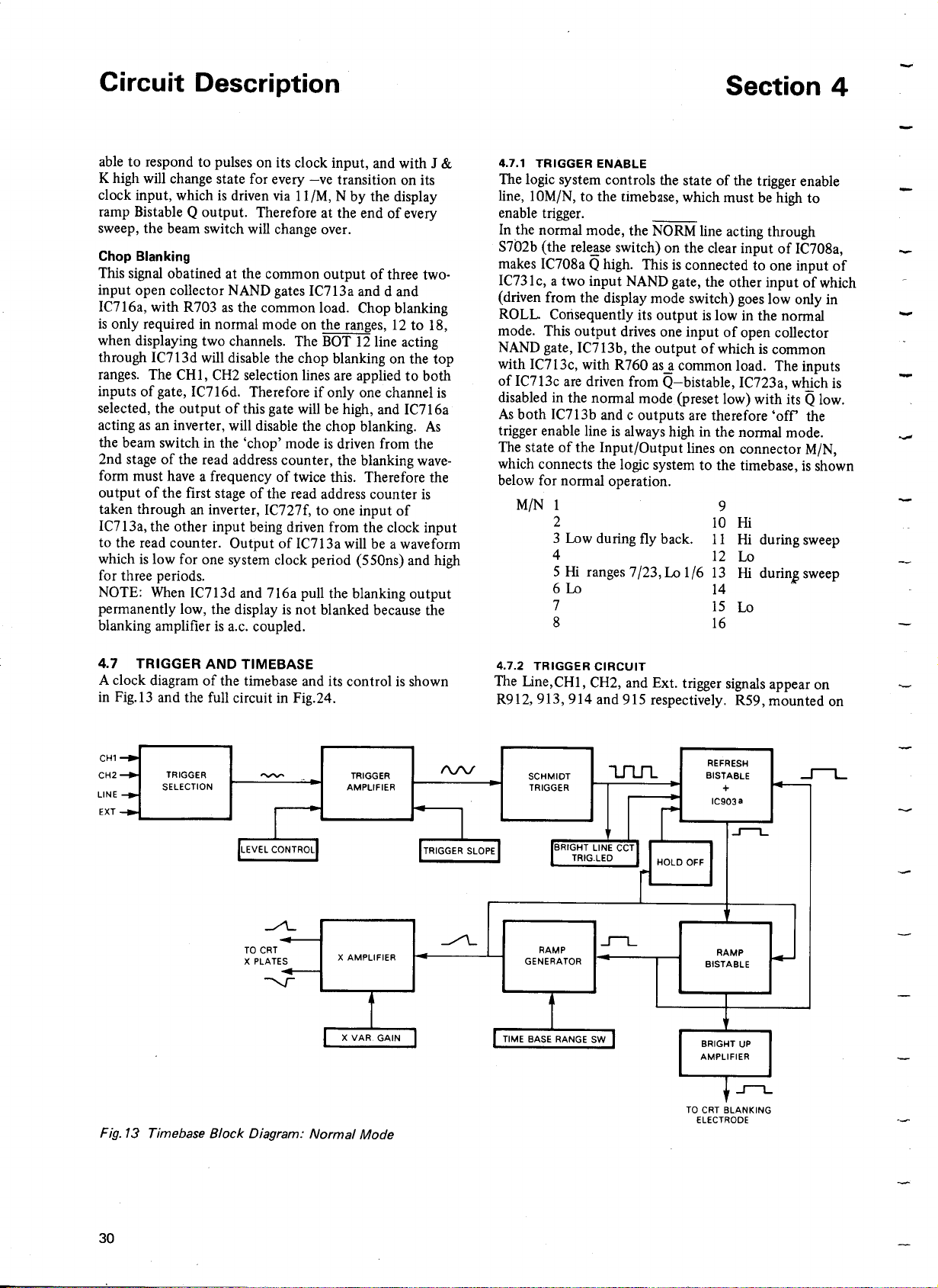
Circuit Description
able to respond to pulses on its clock input, and with J &
K high will change state for every -ve transition on its
clock input, which is driven via 11/M, N by the display
ramp BistableQoutput. Therefore at the end of every
sweep, the beam switch will change over.
Chop Blanking
This signal obatined at the common output of three two-
input open collector NAND gates IC713a and d and
IC716a, with R703 as the common load. Chop blanking
is only required in normal mode on the ranges, 12 to 18,
when displaying two channels. The BOT 12 line acting
through IC713d will disable the chop blanking on the top
ranges. The CHI, CH2 selection lines are applied to both
inputs of gate, IC716d. Therefore if only one channel is
selected, the output of this gate will be high, and IC716a
acting as an inverter, will disable the chop blanking. As
the beam switch in the 'chop' mode is driven from the
2nd stage of the read address counter, the blanking wave-
form must have a frequency of twice this. Therefore the
output of the first stage of the read address counter is
taken through an inverter, IC727f, to one input of
IC713a, the other input being driven from the clock input
to the read counter. Output of IC713a will be a waveform
which is low for one system clock period (550ns) and high
for three periods.
NOTE: When IC713d and 716a pull the blanking output
permanently low, the display is not blanked because the
blanking amplifier is a.c. coupled.
Section 4
4.7.1
TRIGGER ENABLE
The logic system controls the state of the trigger enable
line, lOM/N, to the timebase, which must be high to
enable trigger. _
In the normal mode, the NORM line acting through
S702b (the rele~se switch) on the clear input of IC708a,
makes IC708aQhigh. This is connected to one input of
IC731c, a two input NAND gate, the other input of which
(driven from the display mode switch) goes low only in
ROLL Corisequently its output is low in the normal
mode. This output drives one input of open collector
NAND gate, IC713b, the output of which is common
with IC713c, with R760 as a common load. The inputs
of IC713c are driven from Q-bistable, IC723a, which is
disabled in the normal mode (preset low) with its Q low.
As both IC713b and c outputs are therefore 'off the
trigger enable line is always high in the normal mode.
The state of the Input/Output lines on connector M/N,
which connects the logic system to the timebase, is shown
below for normal operation.
M/N 1 9
2 10 Hi
3 Low during fly back. 11 Hi during sweep
4 12 Lo
5 Hi ranges 7/23, Lo 1/6 13 Hi durin$ sweep
6 Lo 14
7 15 Lo
8 16
4.7 TRIGGER AND TIMEBASE
A clock diagram of the time base and its control is shown
in Fig. 13 and the full circuit in Fig.24.
4.7.2
TRIGGER CIRCUIT
The tine, CHI, CH2, and Ext. trigger signals appear on
R912, 913, 914 and 915 respectively. R59, mounted on
REFRESH
BISTABLE
+
le903"
Page 30

Circuit Description
Section 4
the transformer and connected to the low voltage winding,
forms one arm of a potential divider with R912, resulting
in a±50m V line frequency waveform appearing on R912,
R913 and R914 are the collectorloads of each TR309, in
CHI and CH2 preamplifiers. One centimeter of Y deflec-
tion results in a signal of approximately 25mV on these
loads. R90 and R915 form an approximately 200: 1
attenuator to external trigger signals. RIOIO, RIOll, and
RI008, RI009 are adjusted to take the collector currents
which flow in the CHI, CH2 trigger leads, thus maintaining
the voltage across R913 and R914 near zero in the absence
of Y signals. One of these signals, selected by S900aR,
the frigger source and slope switch, is passed to S901, the
trigger coupling switch, and from there to the base of
TR914. There are four possible signal paths, A.C. coupled
via C907, H.F. rej. via C907 and R916 with C909 by-
passing h.f. signals to ground. (fco ~ 15kHz), LF. rej. via
C908 with R917 bypassing l.f. signals to ground (fco ~
15kHz) or
TR914, acting as an emitter follower, passes the trigger
signal to the amplifier pair, TR915 and TR916, the
potential derived from the level control R7 being passed
via emitter follower, TR917, to the base ofTR916. Thus
the amplified trigger signal appearing between the collect-
ors of TR915 and TR916 contains a d.c. component
determined by the setting of R7. The gain of this
amplifier is determined by R919, 925, 920 and is
approximately 4X. The signal is passed via S900bR to
the input of amplifier, TR901 /TR902. If CH1, CH2 or
EXT are selected the collectors of TR915 and 916 are
connected to the bases of TR901/902 for positive slope,
and TR902/901 for negative slope. If line trigger is
selected, the slope switching is reversed since the line
trigger signal is in antiphase to the a.c. supply. TR901 /
902 form a differential amplifier whose output on the
collector of TR902, drives the Schmitt trigger circuit
TR903/TR904. The gain of amplifier TR901 /902 is
approximately 20 and the output d.c. voltage is adjusted
with the common emitter resistor, RI012.
The function of the trigger circuit, TR903/904 is to
generate a fast negative edge at the collector of TR904,
independent of the rate of change of the applied signal.
The signal appearing on the collector load of TR903 /
R932, is coupled via the network, R933, C902 and R935
to the base of TR904, whose emitter is connected to the
emitter of TR903 and to the emitter resistor, R934. The
emitter coupling introduces positive feedback which
results in a latching action as follows:-
When the base of TR903 is at a low voltage, TR903 is off,
its collector potential is high, therefore the base potential
of TR904 is high turning on TR904. The emitter poten-
tial of TR904 is now higher than the base potential of
TR903. When the base of TR903 goes more positive than
the emitter of TR904, TR903 starts to take some of the
emitter current of TR9Cl4, causing a reduction in its
collector voltage which is communicated to the base of
TR904 thus causing a further reduction in the current
flowing. This effect is regenerative finally leaving TR903
on and TR904 off. The base potential of TR904 is now
O.e.
coupling.
below that of TR903. As R932 is small, the change in
base potential of TR904 is small (~600m V between these
two conditions) so that an a.c. signal of greater amplitude
than this applied to the base of TR903 (if its d.c. level is
adjusted) will cause the circuit to alternate in state. Thus
the output of the circuit for any input above a minimum
will consist of a series of equal amplitude pulses. C903 is
a speed-up capacitor used to reduce the fall times of the
output waveform.
4.7.3
BRIGHT·LINE AND TRIGGER INDICATOR
The waveform appearing at the output of the Schmitt
circuit is coupled via R93 7/C904 to the detector circuit,
0901, TR905 and C906. Positive going transitions on
the Schmitt output result in C904 charging up via 0901.
Negative transitions result in the base of TR905 being
driven negative, and C906 is charged negative by the
emitter current of TR905. If no more negative inputs
are applied, C906 charges slowly positive through R939,
until the base-emitter junction of TR906 is forward
biased. TR906 is then turned on and pulls the base of
TR909 negative via R948, turning off TR909, and
switching off the l.e.d., 0916. If a trigger signal amplitude
or level is altered such that the Schmitt trigger generates
pulses again, C906 will be charged negative, TR906 is
turned off and TR909 is turned on causing 0916 to be lit.
TR906 also controls the emitter current of TR911 via
0903. The base biasing network, R950/R949, ofTR911
is controlled by the NORM line via TR9IO. When NORM
is low, TR9IO is on, and the base voltage of TR911 is
approximately 4V positive with respect to the emitter of
TR906, hence when TR906 turns on and saturates,
current will flow in TR911 and its load R970, such that
TR911 will saturate. Its base voltage under these condit-
ions is approx. 1.5V W.r.t. the emitter ofTR906. When
NORM is high, TR91 0 is off and the base voltage of
TR911 is equal to the emitter voltage of TR906, there-
fore no current will flow in TR911 when TR906 is
turned on. TR9IO can be held off by S7 ("Pull for bright
line off' on front panel). The current drawn by TR911
through R970 acts as a d.c. trigger on the time base
bistable in the absence of Schmitt trigger pulses and is
only allowed in the normal mode when S7 is open.
4.7.4
TIMEBASE BISTABLES (REFRESH AND RAMP
BISTABLES)
The refresh bistable consists of TR912 and TR913, cross
coupled via R951 and R95 5 with C915 and C916 as
speed-up capacitors and R953 and R954 as collector
loads. The collector of TR913 drives the inverter, TR908,
via network, R952. C914, R947 and 0900, with the load
resistor of TR908, R944, connected to the+5V logic
supply line. Thus the output at the collector of TR908 is
in phase with the collector of TR912 and is a T.T.L.
compatible signal designated "REFRESH
diagram. A T.T.L. signal on R946 will control the state
of TR907 via network, R946/R945. The collector load
of TR907 is connected to the base of TR912, hence a low
on R946 will cause TR907 to turn on and therefore the
Q"
in the logic
Page 31

Circuit Description
Section 4
timebase bistable TR912 and TRI13 will be reset into the
condition of TR 912 on, TR913 off. The driven end of
R946 is designated as the 'clear' input of the refresh
bistable on the logic diagram. This bistable can be set
(Q output high) by the occurrence of a negative edge at
the output of the Schmitt trigger (collector TR904) via
C90S, and D904 allows the negative pulse to pass if the
junction of R938/R963 is near ground potential. If the
junction of these resistors is at approximately+S.SV,
D904 is reverse biased sufficiently to prevent (hold-off)
the trigger pulses from reaching the bistable input. (See
section 4.7.5 on Hold-Off.) The bistable can also be set
(Q output high) by the d.c. trigger current from the bright
line circuit via R970. (See section 4.7.3 on Bright line.)
This current is also blocked by the hold-off voltage while
junction R938/R963 is high.
Assume that the bright line circuit is off, (no current in
R970), the hold-off voltage is low, TR912 is on, TR913 is
off and the Q output of IC903b (Ramp B/S) is low. A
single negative transition at the output of the Schmitt
trigger will cause TR912 to go off, TR913 to go on, and
the Refresh Q output to go high. This output acts on
three gate inputs, IC904c, IC906c and IC902d. For
normal operation the table in section 4.7.1 shows that
IC902d and IC906c have one input low (12N) therefore
their outputs are permanently high and Refresh Q has no
effect. Only IC904c is enabled (IC904d+IC904c form a
2 line to one line selector controlled by the NORM line)
consequently when 10 of IC904 goes high, the common
output (load R968) is pulled low causing a negative edge
on the clock input of bistable, IC903b (Ramp B/S).
Preset of 903b is always high, 'clear' is controlled by
TR919 and is high until the end of sweep, J and K inputs
are both high (low on 12N drives the output of IC906
high). These are the conditions required to cause outputs
Q,Qof IC903b to reverse on a negative going clock edge.
Q output therefore goes from low to high, and driving
through inverter, IC90Sa, turns off TR920 (voltage across
base resistor, R961, falls to zero). The timing capacitor
selected by the timebase range switch is now free to
charge positively (see section 4.7.5 for Ramp Generator).
The Q of the ramp B/S (IC903b) also acts on two other
gates, IC902c and IC902b, both two input NAND gates.
(Operation of IC902b is described in the HOLD-OFF
section.) Because 12N is low, the output oflC902d will
be high, so one input of IC902c is high. When Q-IC903b
goes high the output of IC902c goes low, driving IC902a
output high. This supplies current to the bright-up
amplifier (mounted on the Power Supplyp.c.b.) via R971
and a coaxial lead, causing the C.r.t. beam to be unblanked
at the start of sweep.
The ramp generator output (emitter of TR923) goes
positive at a rate determined by the time base range switch,
reducing the negative base voltage on TR919 via the poten-
tial divider R973/R974, and eventually when the emitter
ofTR923 reaches + IIV, TR919 is turned on, pulling
!!:le'clear' input of lC903b low, causing Q to go low and
Q high. ('clear' input of IC903b is connected to N3 into
the logic system but no pull-down input occurs on this
line in the normal mode.) When Q goes low, TR920 is
turned on via IC90Sa, discharging the timing capacitor.
The NORM line (6N) connected to IC90Sb causes its out-
put to be high (high on NORMal), enabling three gates,
IC902b, IC904b and IC904c. This output also turns on
the hold-off circuit via TR918.
The output of IC904b (load resistor, R909) goes low
when the Ramp B/S is reset, clocking IC903a. Conditions
on IC903a are 'clear' high, 'preset' high (see note) J high,
K low andQhigh. The negative transition of the clock
input will cause Q to go low, turning on p.n.p. transistor,
TR907, via R946, and so pulling the base of TR912
positive, turning TR912 on, TR913 off, and Refreshed
Q output low. This is connected via 13N to the logic
system, and controls the 'clear' inputs of bistables, IC734a
and b. When Q Refreshed goes low, IC734a and bare
cleared and the Q output of IC734a drives the 'clear' in-
put of IC903a low via interconnection 14N, returning it
to the quiescent state.
NOTE: On all ranges below SOils/cm to the slowest
available range on normal (200ms/cm), a reset pulse will
occur on ISM prior to the end of sweep. This positive:...
going pulse acting via inverter, IC904a, causes IC903a Q
output to go low, thus resetting the Refresh B/S. which
in turn clears bistables, IC734a and b, driving Q-IC734a
low and via interconnection 14N, clearing IC903a. The
clear input is still preset when the ramp B/S IC903b is
reset by TR919 and therefore the clock pulse generated
by IC903b cannot set IC903a again.
4.7.5 HOLD-OFF CIRCUIT
The NORM line is inverted by IC90Sb (output
high on nqrmal), turning on TR918, connecting one side
of the hold-off capacitor (selected by S6dB) to ground,
and making an input (5) of the NAND gate, IC902b, high.
The other input of this gate is driven high by the Ramp
B/S Q output when the ramp is running. Therefore the
output of the IC902b goes low during the sweep and the
output of IC90 I a will be driven high, cutting off D912
and diverting the current passing through R962 into D902.
This current will charge the hold-off capacitor selected by
S6dB, moving the junction of R963, D902 and R938
positively so that D912 and D911 are turned on when the
capacitor voltage reaches+SV plus two diodes forward
bias potentials. (+ 6.2V approx.) This voltage acting
through R938 drives the junction of C90S and D904
positively so preventing trigger pulses from the Schmitt
trigger reaching the refresh bistable. At the end of sweep
the Q output of the ramp bistable goes low, and drives the
output of IC90la low. D902 is cut off and the hold-off
capacitor is discharged slowly from+6.2V until at
approximately 0 volts, D902 again conducts. Therefore
trigger pulses are prevented from starting another sweep
for a time sufficient to enable the timing capacitor to
discharge completely.
~7~ RAMP GENERATOR
This can use two timing networks, RI007 and C923 or
the resistor and capacitor selected by the time base range
switch, S6. The selection is controlled by the TOP 6 and
Page 32

Circuit Description
NORM lines acting on IC905c. In normal mode operation,
NORM is low and IC905c output is high. The state of
TOP 6 has no effect. TR931 is turned on and TR930 is
turned off by the differential signal applied from IC905c/
905d via level shifting networks, R1002/R1003 and
R1006/R1005. TR931 pulls the gate of Le.t., TR929.
low (-IOV approx.) turning it off, and gate of Le.t.,
TR928, is held by D909 and R1000 at a potential near its
source voltage, so that this f.e.1. is turned on. This
connects the Rand C selected by the time base range
switch, S6, to the input of the ramp generator. Timing
network, R1007 and C923, is selected in 'refreshed' and
'roll' operation on ranges, 7/23, by NORM and TOP 6
being high. However TOP 6 goes low on ranges, 1/6, so
that the timebase range switch Rand C is always used on
these ranges. The ramp generator is a bootstrap circuit
consisting of TR921, TR922, TR923 and D905. The
timing resistor is connected from the junction of D905
and R978 to the timing capacitor, the other end of which
is earthed. The junction of the resistor-capacitor timing
network is connected to the base of TR921 via TR928
or TR929.
The voltage difference between the base of TR921 and
the ramp O/P, TR923, is about+0.6 volts, and D905 is
a 8.2 V zener diode whose bias current is supplied by
R977. Consequently there is a voltage difference across
the timing resistor of approximately IOV. The current
flowing in this resistor will flow into either TR920 (if it
is turned on) or the timing capacitor. If TR920 is on (Q
ramp B/S is low) the timing capacitor cannot charge and
the ramp output (emitter TR923) remains at approx.
+
0.6V above earth. When TR920 turns off at the start
of sweep, current flowing in the timing resistor starts to
charge the capacitor positively. As the voltage gain
between the base of TR921 and the emitter of TR923 is
very nearly 1, the voltage across the timing resistor will
remain essentially constant, thus maintaining a constant
charging current into the capacitor and therefore a linear
increase of voltage against time at the output of the
circuit. At the end of sweep when the ramp O/P voltage
is approx.+11V the Q of the ramp B/S goes low. TR920
is turned on and rapidly discharges the timing capacitor,
bringing the ramp output voltage back to+O.6V.
4.7.7 X
TR924 and TR927 form a p.n.p. differential amplifier
whose gain is controlled by the network, R987, R988,
R6, R990 and R991. The base of TR924 is driven by the
ram p generator and the base potential of TR927 is con-
trolled by the X shift potentiometers, R8A and R8B.
Preset controls, R988 and R990, are set so that as R6 is
varied from maximum resistance to minimum, the gain is
changed by 10 times. As the dynamic range of this
amplifier is then only approx. 1.5V under these condit-
ions, D913 and D914 are required to protect TR924 and
TR927. The mixed sweep plus shift signal produced by
this stage at its output loads, R983 and R998, drives the
differential high voltage amplifier, TR925/TR926, whose
collectors are connected via R985/R992 to the X plates of
the C.r.t.
OUTPUT AMPLIFIER
4.7.8
OPERATION IN THE REFRESHED MODE
Conditions at Logic/timebase interface M/N are:
1 9
2
3 Low during display
ramp fly back
4
5 TOP6 13
6Hi
7
8 16 Ramp start signal
In this mode the display ramp B/S, IC903b, is controlled
from the store, but the refreshed bistable, TR912/3, is
under control of the incoming trigger signals as in the
normal mode.
Assume that no trigger signals are occurring. The ramp
start signal from the store on M/N 16, passes through gate,
IC904, to the clock input of the display ramp B/S, setting
Q high and via IC905a, drives off the ramp gate transistor,
TR920, and starts the sweep.
The NORM line being high selects timing component's RI007,
C923 via IC905c, d and TR928 to 931. This is a sweep of
100J.ls/cm. A RAMP RESET signal from the store will
occur on M/N3 before the analogue ramp reset transistor,
TR919, is turned on by the increasing ramp voltage. This
reset pulse ~cting on the 'clear' input of IC903b drives
Q-IC903b low, thus turning on TR920 and discharging
the timing capacitor, C923. On timebase ranges 1J.ls/cm
to 50J.ls/cm, the TOP6 line (M/N5) acting via IC905c, d,
and TR928 to TR931, selects the normal timing R's and
Cs, and therefore the sweep speed is that set by the time·
base range switch. The analogue ramp reset transistor,
TR919, may now be turned on by the increasing ramp
voltage before the store generates a ramp reset signal.
Thus only a portion of the store contents may be
displayed on the c.r.t. on these ranges.
If a trigger signal occurs, the refresh bistable, TR912/3,
is triggered as in the normal mode, by a negative step on
the output of the Schmitt trigger driving off TR912 and,
setting the refresh bistable Q (collector TR908) high.
This removes the 'clear' inputs to the dual D type bistable,
IC734a and b, making IC734b sensitive to the next P4
E.ulseon its clock input. This drives Q-IC734b high, the
Q of IC734a going low drives the output of gate, IC734b,
high. This is the ENTER DATA line. Pulses from the
range divider can now pass through gate, IC732, to clock
the write address counter and also generate store write
cycles. Q-IC734agoing high removes the 'clear' input
from IC903a making this bistable sensitive to the STOP
signal generated by the store after 1024 new data words
have been loaded. This signal acting via IC904a on the
preset input of IC903a, setsQlow, turning on TR907
Hi after release
10
Lo after 'Store' and trigger
Hi during display ramp
11
12 TOP6.REF. LOCK 100%
Hi after trigger
Lo after 'Stop'
14
Stop (Storefull) signal
15
Page 33

Circuit Description
Section 4
which in turn, pulls the base of TR912 positive thus
resetting the refresh bistable, TR912/3. The refreshed
bistable Q output (collector TR908) going low clears
bistables, IC734a and b, driving Q-IC734a high, and this
acting via gate, IC733b, drives the ENTER DATA line low,
inhibiting the entry of new information into the store.
This cycle will repeat for every trigger signal until the
STORE button is pressed and starts a single shot sequence.
This is described in section 4.7.1.
In the refreshed mode the hold-off time delay is not
required. TR918 is turned off by the NORM line (output
of IC905b) going low, and this effectively disconnects
from ground C90, 91 and 92, the hold-off capacitors.
Read/Write interrupt on ranges SOils/cm to Ills/cm. The
changing of the display ramp generator timing components
on these ranges has already been described. Another
special condition applying to these ranges is that the read
cycles must be interrupted to enable information to be
written into the store. On slower timebase ranges (100IlS/
cm and below) read cycles taking 550ns occur every 1100ns
and write cycles taking 550ns can occur no more frequently.
Therefore read and write cycles can be interlaced. On the
SOils/cm to Ills/cm ranges the write cycles occur every
5S0ns, leaving no time for read cycles. The system
adopted is to read the store at a higher speed (S50ns/
address) until a trigger signal requires the store to accept
new information.
The store then writes 1024 new data words at 550ns/
address, and immediately after this two complete reading
sweeps occur before another trigger signal is allowed to
initiate a new writing sequence (see section 4.6.3).
On the ranges SOils/cm to Ills/cm in the refreshed mode
with LOCK FULL STORE button out, the TOP6 REF.
LOCK 100% line M/NI2 will be high. If the Q output of
the refreshed bistable, TR912/3, is low (no write cycles
occurring) the output of gates,IC902d and 906c, will be
high as on the slower time base ranges. Therefore as
IC906c drives high and J and K inputs of the display ramp
bistable, this bistable will continue to respond to ramp
start pulses from the store. However when a trigger signal
switches the refresh bistable Q high during a display sweep,
the output of gate IC902d is immediately driven low,
causing the removal of the display ramp bright-up via
IC902a and c. This is required since the write address
counter will now have control of the store so that store
data out will not be relevant to this displaying sweep.
Also on completion of the display sweep, all three inputs
to gate, IC906c, will be high, driving its output low and
inhibiting any further displaying sweeps until the Q out-
put of the refresh bistable goes low on the completion of
the write sequence.
4.7.9 OPERATION IN THE ROLL MODE
Conditions at timebase/logic interface M/N are as for the
refreshed mode. (See 4.7.8.)
The display ramp bistable, IC903b, is under the control
of the store previously described for the refreshed mode.
The hold-off circuit, C90, 91 and 92 is disabled as in the
refreshed mode and the timing Rand Care R1007 and
C923. Until the STORE button is pushed, the trigger
enable line is held lbw preventing operation of the
refreshed bistable, TR912/3 , (data is written into the
store because input 5 on IC733b is low, driving the
ENTER DATA line high). After the STORE button is
pressed, the first trigger signal will drive the Q output of
the refreshed bistable, TR912/3, high, removing the 'clear'
input to bistable, IC734a and b. The first P4 clock pulse
after this drives the Q outputs of IC734a and b, high, and
the next P4 pulse drives Q output of IC734b, low.
Further P4 pulses have no effect. The one clock period
wide pulse from Q-IC734b acts on IC605d to allow
through one PS pulse from IC60Sc which acts as a clock
to the trigger point store, IC613, IC621 and IC629,
causing the state of the write address counter at the
instant of trigger to be held in this store.
When a stop signal is generated by the store, this resets
the refreshed bistable as previously described for the
refreshed mode. (See 4.7.8.)
Ranges 100/lSlcm to
The TOP6 line acting through IC90Sc and d, and TR928
to 931, selects the normal timing components for these
ranges. The display ramp bistable is reset by the analogue
ramp reset transistor, TR919, and set by the ramp start
signal from the store. Operation of the refreshed bistable
is not effected. The sweep time is insufficient (except on
the SOils/cm range) to display the total contents of the
store, and the stored trigger point marker may not be
displayed.
On timebase range 7 (lOOlls/cm) after the RELEASE
button has been pressed, the read and write counters are
both clocked at 0.909MHz rate, so that the read and write
addresses are never coincident. This is also true on time-
base ranges SOils/cm to IllS/cm where the read and write
counters are clocked at 1.818MHz. To generate a display
on these ranges, the display ramp start is generated from
the read address counter most significant bit until the
STORE condition is reached. The write address counter
then stops counting so that coincidence pulses are again
generated and can be used to start the display ramp.
4.8 D/A
Referring to the circuit diagram, Fig.25, the D/A converter
is provided in a single integrated circuit, IC745. The
latched eight bit binary outputs from the store, D1 to D8,
are applied to the inputs, pins S to 12, and determine the
output current from pin 4 as a proportion of the input
reference current to pin 14. The reference input is fed
through R729 from the zener diode, D701. R730 provides
fine adjustment of this current to set the full amplitude of
the analogue output.
The output from the D/A convertor is in the form of a
step waveform which follows each successive change of
digital input. The purpose of the subsequent dot joiner
circuit is to convert this into a series of straight lines
joining these successive levels.
As the D/ A output level settles to a new value, amplifier
IC744 detects its difference from the dot joiner output,
and sets a voltage via sampling switch, TR707, on a
storage capacitor, C707. This voltage is sufficient to drive
1/lS/cm
CONVERTER AND DOT JOINER
Page 34

Circuit Description
Section 4
the integrating amplifier, IC743, to correct the error by
the time the next sample is taken.
In more detail, the gain of IC744 and of the complete
system is defined by the input resistor, R799, the shunt
feedback resistor, R736 and the voltage divider, R751,
and R734. The preset potentiometer, R774 with R733,
provides a zero setting control to centre the displayed
waveform. The output of IC744 is buffered by emitter
follower, TR704, to drive the 'hold' capacitor C707
through the sample switch, TR707.
The data from the store is latched by P5 pulses, and the
D/A
converter and IC744 are allowed to settle before
TR707 is switched on during a P4 pulse. These pulses are
a.c. coupled by C709 into the base of the saturated switch,
TR705. This transistor is normally conducting so that
D702 holds the gate ofTR707 near to -IOV. TR707 is
thus non conducting. During the P4 period the drive to
C709 goes negative, TR705 is turned off and its collector
rises toward+5V. The emitter follower, TR706, takes
the gate of TR707 rapidly toward+5V until its collector-
base junction clamps at OV. In this condition TR707
conducts. At the end of the P4 period, TR705 is turned
on and D702 returns the gate potential rapidly to -1 OV.
TR709 and TR708 generate a similar but inverted drive
waveform which is applied via C712 to C707 to compen-
sate for the inherent gate to source capacitance of TR707
which injects an unwanted portion of the gate switching
signal into the storage capacitor. The -10V line is defineJ
by the zener diode, D703.
The integrator formed by TR743 can be considered to
operate in its simplest form when Le.t. switch, TR712, is
open. In this condition the rate of change of output
voltage for a given input voltage is determined by the in-
put resistor, R750, with R785 and the feedback capacitor,
C714. The input voltage from C707 is buffered by the
emitter follower, TR71O. R785 is used to adjust the out-
put slope so that the detected error is reduced to zero at
the next P4 sample period. If R785 is mis-set, the output
will overshoot or undershoot in response to a step change
of input but when set correctly the system will balance in
one sample period.
The above condition with TR714 on and TR712 off, holds
for the display of single trace information on the top 6
time base ranges. In this mode, readout is taken on every
clock pulse, P4 pulses are applied directly to C709 and the
slope defined by C714 and R750 corresponds to 1 clock
period.
For dual trace operation on the top 6 ranges or single
trace operation on the slower ranges, the readout is taken
from alternate clock pulses. The P4 input via C709 is
gated accordingly and TR712 made to conduct. This
introduces C715 into the integrator to slow the output
slope by a factor of two and C713 provides slope adjust-
ment for this mode.
For dual trace operation on the slower timebase ranges,
readout is taken on one clock pulse in four, the P4 input
to C709 is gated accordingly and TR714 is switched off.
R752 and R768 are introduced into the circuit to halve
the rate of change of integrator output voltage again,
R774 providing balance adjustment.
Switches, TR712 and TR714, are controlled by TR713
and TR711 respectively. When on single trace operation
and on the top 6 ranges, both inputs to the base ofTR713
are high and TR713 is biased off and R759 holds the gate
ofTR712 at -10V. When either input goes low, TR713
conducts and its collector voltage is+5V. D707 clamps
the gate of TR712 at OV for conduction.
TR717 operates similarly to turn off TR 714 in all but the
top 6 ranges and dual trace operation, but hold it on,
either in single trace operation or on the top six ranges.
Single trace operation with LOCK. ALT. SAMPLES is
equivalent to dual trace.
4.9
CALIBRATOR
This consists of the adjustable current source, TR934, and
current steering pair, TR933 and TR932. The most signifi-
cant bit from the read address counter (11 on IC640b) is
applied to the base of TR932 via 4N. The read address
counter is clocked continuously at 1.82MHz on range 1/6
and 0.909MHz on ranges 7/23. The 10 bit counter divides
these rates by 1024 giving frequences of 1.78kHz and
8.89kHz at TR932 base and also at the output. The drive
to TR932 causes the current from TR934 to be switched
between TR932 and TR933, where it flows into R1019
and R1020. RI017 is adjusted to give 1V across RI019
and R1020 in series, (1kn) and therefore lOOmV across
R1020 (100n). The current required to do this is 1mA
so that shorting the 1V and lOOmV ca!. out pins together
will cause ImA to flow in the link.
Page 35

Section 5
5.1 GENERAL
The instrument is electrically protected by two fuses as
follows:-
I. The supply line fuse, FS51, mounted on the rear panel
by the line voltage switch. The rating is 500mA Slo-
Blo (Part No.33685) for 220/240 volt supplies and lA
Slo-Blo (Part No.34790) for 115 volt supplies.
2. The+170V fuse, FS501, mounted on the Power
Supply board at the rear of the instrument. Access is
by removing the bottom cover and the fuse rating is
250mA (Part No.32338).
The following sections give information allowing access
to, and removal of, the various printed circuit boards
and assemblies as may be found necessary during fault
finding procedures.
If during fault finding, a component needs replacing it
may be cut from the printed circuit board as close as
possible to the component, leaving the wires protruding
through to the component side of the board. The new
component can then be soldered into position by
attaching it to these protruding wires. This protects
the copper track from damage.
If a fault on a printed circuit board cannot be cleared,
it is recommended that the instrument is returned to
the manufacturer for repair. When faults have been
cleared it is recommended that the test procedure be
implemented to ensure that the instrument conforms
to the specification.
5.2 MECHANICAL ASSEMBLY
5.2.1
LAYOUT
Figures 14 and 15 illustrate the internal layout of the
instrument and show the positions of the majority of
preset components when the top and bottom covers have
been removed. Each cover is retained in position by four
latch fasteners. Each fastener is released by turning it one
quarter of a turn clockwise or counter clockwise.
The POWER SUPPLY board contains the low voltage
power supplies and also the blanking amplifiers. It is
mounted across the rear frame of the instrument behind
the c.r.t.
There are two identical Y PRE-AMPLIFIER boards (note
that components have identical circuit reference numbers
on each of these boards) mounted as 'daughter' boards at
the front of the large ANALOGUE TO DIGIT AL CON-
VERTOR (ADC) board. This board is secured underneath
the C.r.t. and has two other 'daughter' boards associated
with it: the CURRENT SOURCE board which is on the
left hand side nearest the frame, and the DECODING
LOGIC board on the right hand side.
The E.H.T. board incorporates the high voltage power
supplies for the C.r.t. and also the Y OUTPUT AMPLIFIER.
The INTENSITY, SCALE and FOCUS controls are directly
mounted on this board, which is adjacent to the C.r.t. and
one of four boards mounted vertically.
The STORE LOGIC is next to the EHT board.
The TIMING LOGIC board contains also the DOT
JOINER circuit and is the third vertical board.
The TIMEBASE BOARD is mounted on the right hand
side of the instrument and includes also the INTERNAL
CALIBRATOR circuit.
The construction of the instrument has been arranged so
that individual boards and assemblies can be checked and
components changed so far as possible without completely
removing the assemblies from the mainframe or disconnect-
ing cableforms. In the case of the two logic boards this has
been achieved by making them easily withdrawn from
inside the mainframe to be mounted on top of the instru-
ment, as shown in Fig.16. The instrument is then still
fully functional
The following description details the method for removing
the individual assemblies:-
5.2.2
STORE AND TIMING LOGIC BOARDS
The two logic boards are withdrawn as a unit:-
1. Remove the caps from the STORE, RELEASE and the
two LOCK STORE pushbuttons. Remove the knobs
from the MODE, STORED TRIGGER POINT and
DISPLAY MODE lever switches.
2. Remove the 8 screws marked 'A' in Figs.14 and 15.
3. Swing the rear fixing brackets upwards to allow them
to clear the rear mounting plate as the boards are with-
drawn from the front panel. When the unit has been
moved far enough to enable the lever switches and
pushbuttons to clear the frame, withdraw the assembly
from the top of the instrument with the various cable-
forms still attached.
4. Remove the screens from each board, and also unscrew
the screen mounting pillars. This will allow the two
boards to be separated. The two 'L' shaped fixing
brackets should be removed from the top corner of
each board and remounted on the bottom corner using
the rearmost hole and a single nut and screw. The
boards can now be fixed to the top of the instrument
as shown in Fig.16, using the original fixing holes at the
rear, and a single screw through a convenient hole in
the frame at the front. Check that all the connectors
are firmly in position.
Refitting is the reverse of the removal procedure.
Ensure that the 16 way ribbon cable plugs are fully
pushed h9me after fixing the assembly inside the
instrument.
5.2.3
TUBE AND REAR COVER
Removal of the tube is straightforward and provides access
to the track side of the Analogue to Digital Convertor and
E.H.T. boards. Note that access to the rear of the tube
may be gained by removing the moulded plastic cover
which is retained by four fixing screws. The tube is
removed together with its magnetic shield in the following
manner:-
1. Disconnect the E.H.T. lead at the cavity cap connector
at the front of the tube.
2. Disconnect the two trace rotation coil leads at the top
of the power supply board. Mark one of these leads so
that they may be reconnect~d in the correct order.
Disconnect the lead from the tube base to the pin
marked GRID on the power supply board.
3. Remove the tube clamp, secured by three screws.
Page 36

Section 5
CH2 PRE- AMPLIFIER
BOARD
C302 ,C304 ,C306
R370
RIO\\
R.I(Joq
R.lol02
C712 R990 R988 Rl017 REAR MOUNTING
E A G T51
PLATE STAY
Page 37

Section 5
NOTE: LOGIC BOARDS & POWER SUPPLY
SECTION WITHDRAWN FOR MAINTENANCE
4. The tube may now be pulled back so that the faceplate
disengages from the plastic moulding inside the front
panel. Lift the front of the tube and remove the
connector on the base. Withdraw the tube complete
with shield.
5. The tube is a push fit inside the magnetic shield and is
removed together with the trace rotation coil, therefore
as the tube is withdrawn from the shield the trace
rotation coil leads must be fed through the hole in the
shield.
5.2.4
ANALOGUE TO DIGITAL CONVERTOR ASSEMBLY
Access to the trackside of the A.D.e. board is best
achieved by removing the tube as described in section
5.2.3. If the board must be removed it is taken out
together with the Y attenuators, input coupling switches
and shift controls as follows:-
1. Remove the Y attenuator cover by removing the five
fixingscrews and sliding the cover towards the rear of
the instrument to clear the edge of the frame. The
cover may then be lifted out.
2. Remove the knobs from the Y attenuators, shift
controls and input coupling switches. Remove the
nut securing the rotary attenuator switches.
3. Disconnect the 7 power supply leads on the left hand
edge of the board. Disconnect the 4 miniature co-axial
plugs across the centre of the board, SK.P, Q, Rand S,
and the 'BIAS' lead. Remove the 'P' clip securing these
leads to the pillar on the right hand side of the board.
Disconnect the 16 way flat ribbon cable from SK.F on
the right hand 'daughter' board.
4. Remove the 5 securing screws marked B in Fig.14.
Lift the rear of the board and withdraw it from the
instrument.
Refitting the board is the reverse of the removal pro-
cedure, but note that when fitting the securing nut to
the attenuator switches, the switch assembly should
be held with long-nosed pliers to avoid twisting the
switch along its length. The colour code of the power
supply leads may be ascertained by inspecting the
bottom edge of the power supply board; the two
50 volt supplies marked 'Va' and 'Vb' on the A.D.e.
board are interchangeable.
5.2.5
POWER SUPPLY
ASSEMBLY
Normal access to the component side of the board is
possible by removing the tube, and the trackside of the
board is exposed by removing the moulded plastic rear
Page 38

Section 5
cover (4 fixing screws). The board may be removed by
releasing the two screws securing it to the frame and
also the two screws securing the heatsink bar at the
edge of the board to the finned heatsink assembly.
Alternatively the board may be removed as a complete
assembly with the finned heatsink,power transformer,
ON/OFF switch and C5I in the following manner:-
1. Remove rear cover.
2. Remove the two screws, marked 'G' in Fig.I5,
securing the power transformer to the logic
assembly mounting plate.
3. Slacken the clamp, marked 'H' in Fig.I5, and
release the ON/OFF switch actuating rod from the
ON/OFF switch.
4. Remove two screws securing the power supply board
to the frame on the tube side of the instrument and a
further four screws securing the finned heatsink to the
frame. Two fixing screws holding the small panel
bearing the supply line voltage switch and fuse must
also be removed.
5. The rear panel assembly may now be withdrawn
sufficiently to replace most of the components:
complete separation entails disconnecting the two
main cable forms from the power supply board and
five leads associated with the c.r.t.
Refitting is the reverse of removal. Care should be
taken to ensure that the insulating shim between the
power transformer and the logic assembly mounting
plate is correctly positioned and the insulating bushes
fitted to the screws 'G' securing these two parts are
fitted. The clamp linking the supply switch,S5I, to
the front panel should be carefully aligned so that the
switch operates freely without any tendency to stick.
5.2.6
TIMEBASE
Routine access to the timebase board may be gained by
removing the logic boards as detailed in section 5.2.2.
The timebase range switch may alsQ be removed (see 3.
below) and the board itself may be taken out along with
the time base controls (X shift, timebase range, trigger
level, source and coupling and external input socket).
Proceed as follows:-
1. Remove the knobs from the 5 rotary controls and the
cap from the lever switch.
2. Remove the nut securing the EXT. TRIG.B.N.C. socket
and unsold er R9I allowing the socket to be removed.
3. Remove the nut from the bush of the TIM E/CM rotary
switch. Disconnect the 16 way ribbon cable from the
timebase range switch at SK.L on the bottom of the
timing logic board, and also the five leads to the time-
base board at the pins labelled 9, 10,
Remove the single fixing screw holding the rear support
bracket of the switch to the frame. Withdraw the
switch assembly.
4. At the rear of the time base board, disconnect the 4
power supply leads, the twin ribbon cable to the X
plates pins 5 and 6, and remove the fixing screw
securing the board to the rear mounting plate (marked
'E' in Fig.I5).
av,
15 and 16.
5. From underneath the instrument, disconnect and
identify the three screened leads to the pins labelled
SB, CHI trig. and CH2 trig. and the single wire to the
Line trig. pin. Remove the two bottom fixing screws
(marked 'E' in Fig. 14). Remove the rear mounting
plate stay (see Fig.I5). Pull the rear of the board back
between the power transformer and the frame side-
member until it is possible to disengage the rotary
control spindles from their holes in the front panel.
The board may now be withdrawn from the instrument.
5.2.7 E.H.T.
Access to the E.H.T. board is normally obtained by re-
moving the C.r.t. and the two logic boards. If, for some
reason, the board itself must be removed, proceed as
follows:-
1. Remove the c.r.t. the logic board assembly and the
A.D.e. board assembly.
2. Slacken the clamp 'H' (see Fig.I5) and withdraw the
ON/OFF switch actuating rod through the front panel.
3. Remove the knobs from the SCALE, INTENSITY and
FOCUS controls. Remove the small plate in front of
the ON/OFF switch. Disconnect all leads.
4. Release the 3 screws marked 'F' in Fig.I5, and pull the
board towards the rear of the instrument until the
control spindles clear the front panel, and remove the
board from the instrument.
5.3 FAULT FINDING
Faults may be attributed to specific areas of the instru-
ment by following the fault localisation procedure given
in section 5.3.1. More detailed examination of the
analogue circuitry may be undertaken with the aid of the
circuit voltage tables given in section 5.3.2, and the
Control Condition Table illustrated in Fig. 17 will help to
isolate faults in the digital (logic) circuitry.
Certain faults occurring in the digital section of the
instrument (in connection with the manipulation of the
digitised signal and the addressing of the stores) and also
the Analogue to Digital Convertor (A.D.e.) are often
characterised by particular distortions of the displayed
signal in the REFRESHED and ROLL modes. A logical
method of approaching these faults is outlined in section
5.3.3 together with the secondary fault localisation charts
for the stored data path (section 5.3.4) and the A.D.e.
(section 5.3.5).
BOARD
Page 39

Normal Mode
Single Trace
Normal Mode
Dual Trace
Refreshed Mode
Ranges 7/23
Single Trace
(Released)
Refreshed Mode
Ranges 7/23
Dual Trace
(Released)
---~~
Refreshed Mode
Range 1/6
Single Trace
(Released)
Refreshed Mode
Ranges 1/6
Dual Trace
(Released)
Display Ramp
Start
From Refresh
B/S
a
Display Ramp Read Address
Stop Oock Oock Write Address
Analogue
via TR919
I
I
..
From A.A.C.
M.S.B, via M.s.B.via
Delay Circuit
FromA,A.C. 0.909 MHz
Delay Circuit
..
..
Analogue via
TA919
..
0.909 MHz
..
from IC 728a, b,
via gate IC 707
..
1.81BMHz
from PI via
IC 720b ranges
.. ..
Write Address
-
..
..
-
From Range
Divider. see
Table for
freqUency
..
1.818MHz
onal16
..
LS.Bit
- -
-
From Write
Address Counter
lW.A.C.l
I
..
..
I
..
L.S.Bil
Read Address
-
From Aead P4 Pulse at
Address Counter 0.909 MHz rate
lA.A.C.1
EXCEPT
EXCEPT
SO%
From a/s
IC 723a via
gate IC 719
From Aead
Address Counter
(R.A.C.l
SO%
From a's
IC 723a via
gate IC 719 ';ia gate IC 7328
Dot Joiner
Sample&Hold
(SclH) drive
-
-
via gate IC 732a
1
HOLD
P4 Pulse at
0,455 MHz rate
via IC 7258, b,
&
IC 7328
P4 Pulse at
1.818 MHz rate
via IC 725a, b,
&
IC 732a
HOLD )
P4 Pulse at
0.909 MHz rate
Dot Joiner
Time constant conditions
(TC) controls
A B C
- -
-
0
1
0
I
I
0
0
1
1
I
0 0
1
0
1
50% Hold
D
50% Hold drives L.s,B.
1
Write Address high and
sets up Oual Trace
conditions for Aead
Address and Dot
joiner (Condition 1)
50% Hold dri~
I
L.S.B. write address
high.
(Condition 2)
Condition 1
0
Condition 2
Special Y Channel
Functions Beam Switch
Refr"h Mode
Selected on
A'li 19/23
-
-
-
-
Write sequence
stops read. Then
two read sweeps
before trigger is
enabled
"
-
Ramp B/saclocks
IC 708 b, on A1/11
(ALT)
2nd stage A.A.C. drives
IC 708 b, clear to give
chop (A12/181
-
From l.s.B.
W.A.C.
-
From l.s.B.
W,A.C.
Roll Mode
Ranges 7/23
Single Trace
(Released)
Roll Mode
Range 7/23
Dual Trace
(Released)
.
Roll Mode
Range 1/6
Single Trace
(Released)
Roll Mode
Range 1/6
Dual Trace
(Released)
From Coincidence From Coincidence
gate via delay gate via delay
..
From M.s.B.
R.A.C. A.A.C.
..
..
FromM.S.8.
..
0.909 MHz
from I C 728a. b,
via gate IC 707
..
1.B18MHz
fromPl via
IC 720b
.
From Aange
Divider - See
Table for
frequency
..
1.818MHz
on all 6 ranges
..
From \/\tite From Aead
Address
Counter
I
..
..
[
..
Address 0,909 MHz rate
Counter via gate IC 732a
EXCEPT 50% HOLD
From B'S
IC 723a via
gate IC 719
From AAC
EXCEPT 50% HOLD
From
IC 723a via
pte IC 719 IC 732a
1
P4 Pulse at
P4 Pulse at
0,455 MHz rate
via IC 725a, b,
&
IC 7328
1.818 MHz rate
via gate IC 7328
BIS
0.909 MHz
rate via gate
0
I
0
1
I
1
1
0
Condition 1
0
1
1
Condition 2
1
0
0
Condition 1 "STORE" Condition
0
0
1
Condition 2
-
-
Displayed information
is set by W.A.c. until
is reached when
RAC. addresses store.
.
From L.S.B.
W.A.C.
From L.S.B •
W.A.C.
-
-
en
CD
n
_.
r+
o
~
C1I
Page 40

Set supply voltage switch to suit
1.
supply voltage.
Connect supply voltage and switch
2.
on.
Doesfront panel neon lamp light?
YES
Section 5
CHECK
1. Supply Voltage
2. Rear Panel Fuse
3. ON/OFF switch
4. Supply voltage switch
5. Power Transformer
6. Front Panel neon
Are power supplies within limits
given in section 5.4.2?
YES
1.
Set X and Y shift controls
to mid range positions.
Set DISPLAY MODE to
2.
NORMAL
Set Y MODE to CHI
3.
Set TIME/CM to 5ms/cm.
4.
Set TRIGGER SOURCE to
5.
LINE
Set TRIGGER LEVEL
6.
control central.
Advance INTENSITY
control. Is trace obtained?
YES
_NO_
TRACE
0
Is mean
within li
sect 5.3.
YE
Is sweep
on X plat
Y
UTSIDE
IMITS
L
plate potential
mits given in
2?
signalpresent
----I
es?
1. Check supply line voltage
2. Check voltage switch setting
3. Check affected supply
Check
NORM
SKF pin 4 (ADC board)
Check voltage at input to
Y O/P amplifier at SK.Q.
Check voltage at R389.
Check Pre-amplifier
NO- 1. Check input to X amplifier
at R981
2. Check trigger pulses
present at cathode D904.
3. Check
4. Check RAMP B/S Q at
NORM
SK. N pin 6.
IC903 pin 11
is low at
is low at
,-
Is sweep
signal goi
TR513 c
Y
Are c.r.t.
potential
blanking
ng low at
ollector?
electrode
s correct?
1. Check SB output on
NO- timebase board.
2. Check sweep blanking
amplifier on power supply
board.
Page 41

5.3.1
Section 5
(Contd.1
I
Set Y MODE to CHI&CH2
Are two traces obtained?
YES
1..
Set TRIGGER SOURCE to EXT
Ensure TRIGGER LEVEL is
2.
pushed in (bright line on)
Does timebase free run?
YES
Apply 1 volt input from
colibrator with VOLTS/CM. set
at 0,2 V/cm.
Is 5 cm vertical deflection
obtained?
YES
Apply 1 kHz sine wave with
TIME/CM switch at 100/Js!cm.
DO TRIGGER LEVEL and
TRIGGER SOURCE controls
work correctly?
1. Check channel select signal at
SK F pin 3 (Hi on CHI)
2. Check beamswitch circuit
3. Check CH2 Pre-amplifier
.
1. Check signal amplitude at R389
to be 185 mV.
2. Check Y O/P amplifier
3. Check EHT voltage.
1. Check trigger output
from Y Pre-amplifiers
2. Check trigger circuits
3. Check hold-off circuit
YES
Set DISPLAY MODE
switch to REFRESHED
Is display still present? ~NO-
YES
l'
Is sweep s
at input t
at R981?
YE
Is dot joi
voltage at
±
150 m
YE
Check sig
circuit
(0
board).
ignal present
o X amplifier
ner output
SK Y within
V?
nal switch
n A.D.C.
CHECK:
NO- 1. Ramp start pulse at
SKN pin 16
2. Read address counter
clock pulses at IC656
pin 14
3. Read address counter
MSB output at
IC740 pin 9.
4. Delayed ramp start
circuit
Page 42
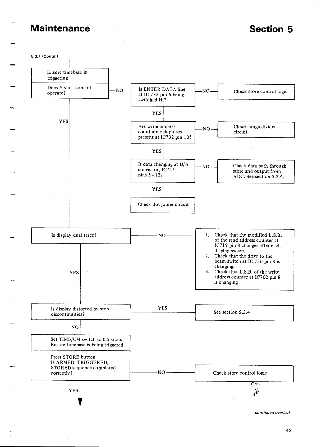
I
Ensure timebase is
triggering
Section 5
Does Y shift control
operate?
YES
Is display dual trace?
YES
-NO-
Is ENTER DATA line
at IC 733 pin 6 being
switched Hi?
YES
Are write address
counter clock pulses
present at IC732 pin 10?
YES
Is data changing at D/A
conyertor,IC745
pins 5 - 12?
YES
Check dot joiner circuit
NO
-NO- Check store control logic
-NO-
-NO-
I.
Check that the modified L.S.B.
of the read address counter at
IC719 pin 8 changes after each
display sweep.
Check that the drive to the
2.
beam switch at IC 736 pin 8 is
changing.
Check that L.S.B. of the write
3.
address counter at IC702 pin 8
is changing
Check range divider
circuit
Check data path through
store and output from
ADC. See section 5.3.4.
Is display distorted by step
discontinuities?
NO
Set TIME/CM switch to 0.5 s/cm.
Ensure timebase is being triggered
Press STORE button
Is ARMED, TRIGGERED,
STORED sequence cOJ!lpleted
correctly?
YES
"
YES
NO
See section 5.3.4
Check store control logic
I
1--_
~
I
Page 43

Set DISPLAY MODE switch to
ROLL.
Press RELEASE button
Section 5
Is display still present?
YES
Does Y shift control operate?
YES
Can two traces be obtained on all
time base ranges?
YES
Press STORE button.
Is ARMED, TRIGGERED,
STORED sequence completed?
YES
When STORE button is pressed
repeatedly, is old information
cleared? (change time base range
before pressing button t9
distinguish new information)
Check ramp start pulse at
coincidence gate OIP IC632
pin 8.
1. Check ENTER DATA is high
at IC733 pin 6
2. Check store control logic.
Check read clock pulse adder
(lCnl)
Check ROLL trigger enable
circuit.
Page 44
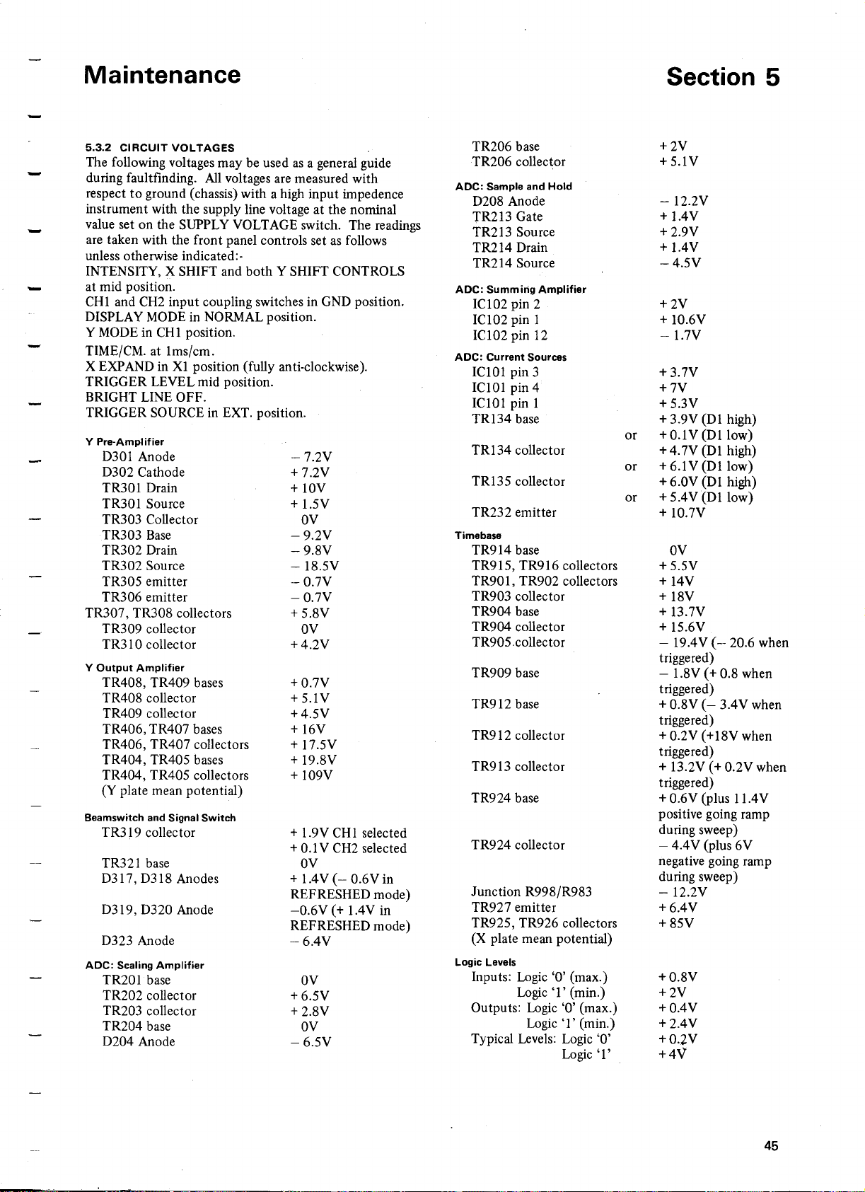
Section 5
-
5.3.2 CIRCUIT VOLTAGES
The following voltages may be used as a general guide
during faultfinding. All voltages are measured with
respect to ground (chassis) with a high input impedence
instrument with the supply line voltage at the nominal
value set on the SUPPLY VOLTAGE switch. The readings
are taken with the front panel controls set as follows
unless otherwise indicated:-
INTENSITY, X SHIFT and both Y SHIFT CONTROLS
at mid position.
CHI and CH2 input coupling switches in GND position.
DISPLAY MODE in NORMAL position.
Y MODE in CHI position.
TIME/CM. at lms/cm.
X EXPAND in Xl position (fully anti-clockwise).
TRIGGER LEVEL mid position.
BRIGHT LINE OFF.
TRIGGER SOURCE in EXT. position.
Y Pre-Amplifier
D30l Anode
D302 Cathode
TR30l Drain
TR30l Source
TR303 Collector
TR303 Base
TR302 Drain -9.8V
TR302 Source
TR305 emitter -0.7V
TR306 emitter -0.7V
TR307, TR308 collectors
TR309 collector
TR3l0 collector
Y Output Amplifier
TR408, TR409 bases
TR408 collector + 5.lV
TR409 collector
TR406, TR407 bases +16V
TR406, TR407 collectors
TR404, TR405 bases
TR404, TR405 collectors
(Y plate mean potential)
Beamswitch and Signal Switch
TR3l9 collector + 1.9V CHI selected
TR32l base
D3l 7, D318 Anodes
D3l9, D320 Anode
D323 Anode
ADC: Scaling Amplifier
TR20l base
TR202 collector
TR203 collector
TR204 base
D204 Anode
-7.2V
+7.2V
+ lOV
+ l.5V
OV
-9.2V
- l8.5V
+5.8V
OV
+4.2V
+0.7V
+4.5V
+ l7.5V
+ 19.8V
+ 109V
+ 0.1 V CH2 selected
OV
+ lAV (- 0.6Vin
REFRESHED mode)
-0.6V (+ lAV in
REFRESHED mode)
-6AV
OV
+6.5V
+2.8V
OV
-6.5V
TR206 base +2V
TR206 collector
ADC: Sampleand Hold
D208 Anode
TR213 Gate
TR213 Source +2.9V
TR2l4 Drain + lAV
TR2l4 Source
ADC: Summing Amplifier
IClO2 pin 2
ICl02 pin 1 + lO.6V
IClO2 pin 12
ADC: Current Sources
IClOl pin 3
IClOl pin 4
ICIOl pin 1
TR134 base
or +O.lV(Dllow)
TR134 collector
or
TR135 collector
or + 5AV (Dl low)
TR232 emitter
Timebase
TR9l4 base
TR9l5, TR9l6 collectors
TR90l, TR902 collectors
TR903 collector
TR904 base
TR904 collector
TR905.collector
TR909 base
TR912 base
TR9l2 collector
TR9l3 collector
TR924 base
TR924 collector
Junction R998/R983 - l2.2V
TR927 emitter
TR925, TR926 collectors
(X plate mean potential)
Logic Levels
Inputs: Logic '0' (max.)
Logic '1' (min.)
Outputs: Logic '0' (max.)
Logic '1' (min.)
Typical Levels: Logic '0'
Logic '1'
+ 5.lV
- l2.2V
+ lAV
-4.5V
+2V
- 1.7V
+3.7V
+7V
+5.3V
+ 3.9V (D! high)
+ 4. 7V (Dl high)
+ 6.1 V (Dllow)
+ 6.0V (Dl high)
+ 10.7V
OV
+5.5V
+14V
+18V
+ 13.7V
+ l5.6V
- 19AV (- 20.6 when
triggered)
- 1.8V (+ 0.8 when
triggered)
+0.8V(- 3AVwhen
triggered)
+ 0.2V (+18V when
triggered)
+ l3.2V (+ 0.2V when
triggered)
+ 0.6V (plus 11.4V
positive going ramp
during sweep)
- 4AV (plus 6V
negative going ramp
during sweep)
+6AV
+85V
+0.8V
+2V
+OAV
+2AV
+O.ZV
+4V
Page 45

Section 5
5.3.3
DATA FAULTS
When tracing faults which cause gross distortions (steps,
discontinuities, etc.) of the display in the REFRESHED
and ROLL modes, it is helpful to distinguish between
three cases:
1. Addressing errors. These will occur at particular
positions across the screen in the X direction regard-
less of the setting of the vertical shift controls.
2. Data errors. These will occur at specific positions up
the screen in the Y direction regardless of the Y shift
control.
3. Timing errors. These will usually be spikes or notches
occurring in a fairly random fashion, but often affected
by the timebase range switch and the store controls,
interaction between the traces may also occur.
Address lines may be verified by checking for a true
binary sequence, that is, by ensuring each bit is
changing at twice the frequency of the next most
significant bit. This may be done at the address inputs
of the stores by switching to the ROLL mode with the
timebase range switch at 50fJ.s/cm. In this condition the
stores are continuously addressed by the write address
counter only. Pressing the LOCK FULL STORE push-
button selects the read address counter only.
The eight data lines may be checked from the output of
the analogue to digital convertor at SK.F, through the
'data in' latches, IC618 and IC619, the eight store
packages, 'data out' latches IC650 and IC659, to the
digital inputs of the digital to analogue convertor, IC745.
Note that the sense of the data is inverted after the input
latches. If a triangle or sawtooth (as obtained from an
oscilloscope ramp output for example) waveform is used
as an input signal, the data will approximate to a binary
sequence as with the address counters, and may be easily
yerified. With the instrument in the ROLL and the time-
base set fo 100fJ.s/cm., the read and write address counters
will be running at the same rate, so that the data output
rate from the store will be the same as the data input rate,
thus simplifying checking. Note that even in this condition,
however, the output data cannot be compared directly with
the input data since the relative timing between the two
(due to the time that the data is held in the store before
being read out) will be arbitrary.
Timing errors must be found by checking the various
clockpulses and control signals around the store and A.D.C.
against the timing diagrams given in this section and also
the circuit description section. When inspecting fast pulses,
a fast rise-time oscilloscope must be used (say better than
IOns) together with an appropriate low capacitance probe
and earth lead. The logic devices used are from the well
known 'T. T.L.' (Transistor-Transistor Logic) family and
typical propagation delays for each type of device may be
obtained from manufacturer data sheets.
Page 46
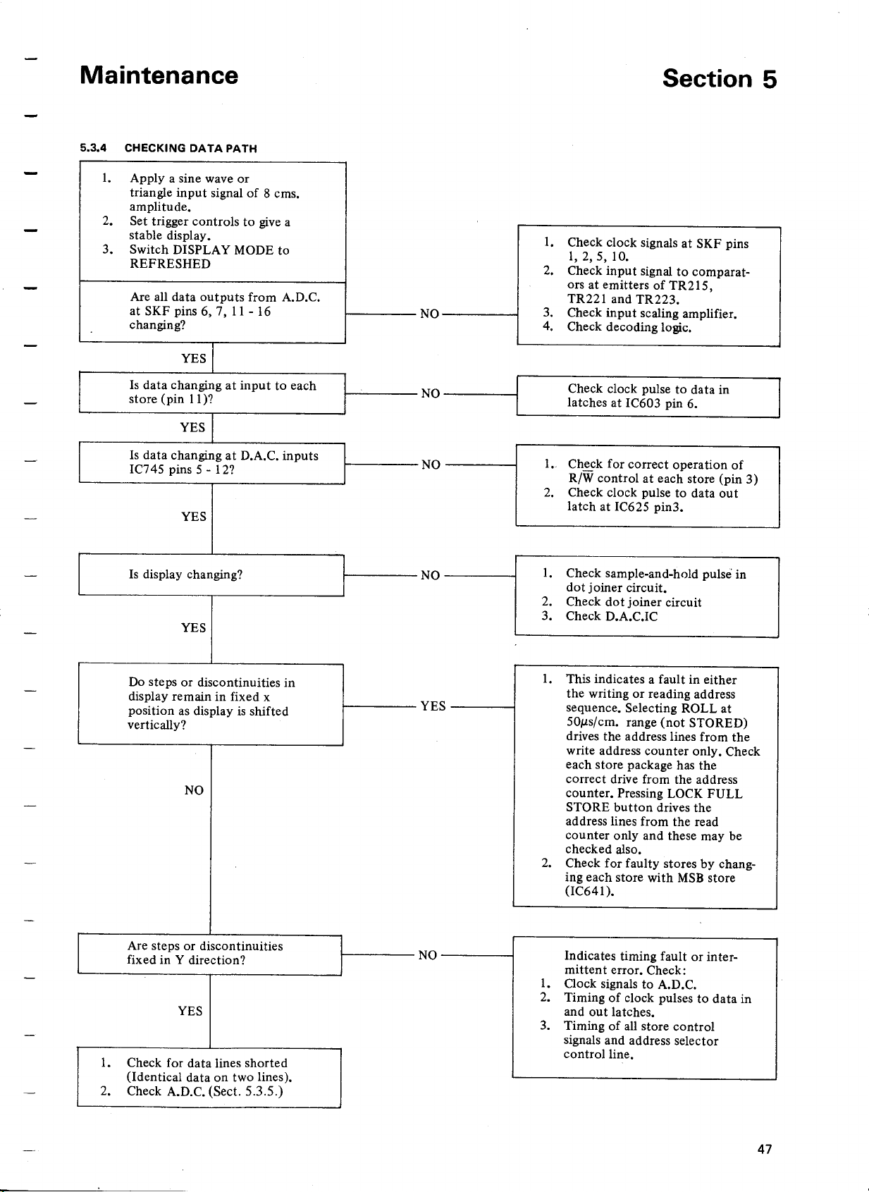
1.
Apply a sine wave or
triangle input signal of 8 cms.
amplitude.
Set trigger controls to give a
2.
stable display.
Switch DISPLAY MODE to
3.
REFRESHED
Are all data outputs from A.D.C.
at SKF pins 6, 7, 11 - 16
changing?
YES
Section 5
1. Check clock signals at SKF pins
1,2,5, 10.
2. Check input signal to comparat-
ors at emitters of TR2l5,
TR22l and TR223.
3. Check input scaling amplifier.
4. Check decoding logic.
Is data changing at input to each
store (pin ll)?
YES
Is data changing at D.A.C. inputs
IC745 pins 5 - l2?
YES
Is display changing?
YES
Do steps or discontinuities in
display remain in fixed x
position as display is shifted
vertically?
NO
Check clock pulse to data in
latches at IC603 pin 6.
1. Ch~k for correct operation of
R/W control at each store (pin 3)
2. Check clock pulse to data out
latch at IC625 pin3.
1. Check sample-and-hold pulse in
dot joiner circuit.
2. Check dot joiner circuit
3. Check D.A.C.IC
1. This indicates a fault in either
the writing or reading address
sequence. Selecting ROLL at
SOils/cm.
drives the address lines from the
write address counter only. Check
each store package has the
correct drive from the address
counter. Pressing LOCK FULL
STORE button drives the
address lines from the read
counter only and these may be
checked also.
2. Check for faulty stores by chang-
ing each store with MSB store
(IC64l).
range (not STORED)
Are steps or discontinuities
fixed in Y direction?
YES
Check for data lines shorted
1.
(Identical data on two lines).
Check A.D.C. (Sect.
2.
Indicates timing fault or inter-
mittent error. Check:
1. Clock signals to A.D.C.
2. Timing of clock pulses to data in
and out latches.
3. Timing of all store control
signals and address selector
control line.
5.3.5.)
Page 47

With the DISPLAY MODE set to
REFRESHED apply a sine wave
or triangle input signal. Set the
amplitude and trigger controls so
that a single half cycle of the
input signal is displayed from
positive peak to negative peak as
in fig 18 at
Section 5
Is signal correct at the emitter of
TR2IS? This should be inverted
in sense and at approx. 3.7 volts
peak amplitude for full screen
deflection.
YES
Are first two data bits (DI, D2)
changing in correct manner?
I
(see fig 19 b&c).
YES
Is signal waveform at emitter of
TR221 correct? (see fig 19d).
YES
Are data bits D3, D4, D5 correct?
(see fig 1ge, f&g)
YES
--
INC
AMPLI
DIST
WAY
ORRECT
TUDEOR_
ORTED
EFORM
I. Check scaling amplifier circuit and
adjustment.
2. Check sample and Hold circuit.
1. Check comparators
2. Check reference voltages
3. Check decoding logic
I. Check first two switched current
sources, TRI36 and TR139.
2. Check first summing amplifier.
I. Check comparators
2. Check second row reference
voltages.
3. Check decoding logic.
-
Is signal waveform at emitter of
TR223 correct? (see fig 19h)
YES
Are data bits D6, D7, D8
changing?
YES
Are errors (notches)
present in the display at
fixed Y levels?
NO
,-
f-YES-
Does pat
each qua
YE
tern repeat in
rter of screen?
I. Check remaining three switched
current sources, TR144, TRI47 and
TR ISO.
2. Check second summing amplifier.
I. Check third row comparators.
2. Check third row reference voltage
chain
3. Check decoding logic
1. Check first two current
sources
2. Check offset and gain of
first summing amplifier.
3. Check first row
comparators.
4. . Check second row
reference voltage chain.
Page 48

Does pat
four tim
vertical
YE
1.
Chec
2.
Chec
volt
Chec
3.
latc
tern repeat
es per cm. of
deflection?
k final row comparators
k third row reference
age chain
k timing of decoding logic
h pulses
NO- second summing amplifier
1. Check last three current
sources TR144, TR147,
TR150.
2. Check offset and gain of
3. Check second row
comparators.
4. Check third row reference
voltage chain.
Are regular fixed height steps
visible as fig 18b?
NO
Check timing and frequency of all
clock signalsand latch pulses.
Check data path through store
(see sect. 5.3.4)
Check data path through store
for missingor shorted data lines.
Page 49

BI
DATA BIT MISSING
STEP HEIGHT
4 cms
2 cms
1 cm
5 mm
2.5 mm
1.2 mm
.6 mm
.3 mm
Section 5
DATA LINE
01
02
03
04
05
06
07
08
FIRST TWO SWITCHED CURRENT SOURCES IN ADC
NOT WORKING (TR136 AND TR139)
OR
FIRST SUMMING AMPLIFIER FAUL TV.
Similar fa.ults for remaining three current sources
and second summing amplifier but step height 4 times
smaller and pattern repeats over each quarter of the
screen.
Page 50

INPUT SIGNAL AT EMITTER
OF TR215
I
1
1
1
I
1
11
11
m
1
11
1
11
I
11
I
1
I
JfU1
1
11
1
11
I
11
I
I I
I
•
II1 1 11
II1II1 1
I I 1II
1
I I I I I
gAI1i
..•
.,
11
11
JL
I I I I
I I
I I I I I
1 I
J
,,,11
1
1
r-
I
I
I
H
GI
HI
DI
El
FI
WAVEFORM AT EMITTER OF TR221
OUTPUT OF FIRST SUMMING AMPLIFIER
D3 OUTPUT (SK.F PIN 14)
D4 OUTPUT (SK.F PIN 13)
D5 OUTPUT (SK.F PIN 12)
WAVEFORM AT EMITTER OF TR223
OUTPUT OF SECOND SUMMING AMPLIFIER
Page 51

Section 5
5.4
CALIBRATION PROCEDURE
The calibration procedure is detailed below. Note that
any calibration adjustments found necessary must not be
made until a 15 minute warm-up period has elapsed. The
locations of the various preset components are shown in
Figs. 14 and 15.
5.4.1 TEST EQUIPMENT REQUIRED
1. Multimeter to measure up to 1500 volts with better
than 20H2 per volt impedence. Accuracy to be within
±
2%.
2. Variable Autotransformer (Variac, etc.) Output voltage
range 200 - 270 volts at lA with a.c. r.m.s. volt-
meter.
3. Function Generator with frequency range of O.IHz to
10kHz, preferably with sawtooth output.
4. Digital Voltmeter with 30. digit display and fm V basic
resolution. Accuracy to be within ± 0.2%.
5. Source of Time and Voltage Calibration signals, to
cover the range O.lps - 0.5s. and 25m V - 100V.
6. Square-wave generator to provide 500kHz flat top
square wave with amplitude adjustable between 25mV
and 1 volt. Risetime to be less than 5ns.
7. Constant amplitude r.f. sine-wave generator to cover
the range 500kHz to 15MHz with a 50kHz reference
frequency. Output amplitude 25mV to 5 volts pk-pk
when terminated with son load. Amplitude accuracy
over the frequency range to be within ± 3%.
8. Capacitance standardiser. IMn/28pF with RN.C.
connections.
9. son B.N.e. through-tennination.
10.E.H.T. meter to measure 3kV.
11.Frequency Counter to measure 1kHz at 1 volt.
5.4.2 POWERSUPPLY VOL TAGES
1. Set the INTENSITY control to minimum.
2. Set the SUPPLY VOLTAGE switch on the rear panel
to suit the available supply. Using the autotransfonner,
set the supply to the instrument to within±1% of the
selected nominal voltage.
3. Check that the POWER neon, N51, is lit and that the
SCALE control varies the graticule illumination.
4. Check the voltages with respect to the chassis at the
pins on the lower edge of the power supply board as
follows:-
limits voltage
pin min. max.
+5 iO is
-20 -19 -21
-6 -5.5 -6.5
+ 12 11.4 12.6
+20 19 21
+ 170 155 185
5. Measure the voltage across C40.1(see Fig.15) on the
E.H.T. board and adjust R409 (SET E.H.T.) to bring
this to 185V with the supply voltage adjusted as in 2.
above.
6. Measure the voltage at the - lkV pin on the E.H.T.
board (near C403). This voltage should be between
- 950V and - 1050V with respect to the chassis,
check that it does not vary by more than 10V when
the supply voltage to the instrument is varied by±10%
of the nominal voltage selected with the SUPPLY
VOLT AGE switch.
7. Check that the voltage on the '+ 3kV' pin at the rear of
the E.H.T. board (to which the cable from the c.r.t.
cavity cap connector is fitted), is greater than 2.5kV
relative to chassis.
5.4.3 GEOMETRY
1. Set the MODE switch to NORMAL, the TIME/CM.
switch to Ims/cm. and ensure the TRIGGER LEVEL
control is pushed in ('Bright Line' position). With the
INTENSITY control advanced approximately half way
and the Y MODE switch in the CHI and CH2 position,
obtain two traces on the screen.
2. Adjust the FOCUS control in conjunction with R41 7
('ASTIG') on the E.H.T. board to obtain clear traces.
3. Adjust the TRACE ROTATION control, R529, on the
rear panel to align the traces with the horizontal
graticule lines.
4. Apply a 1kHz sinewave to one channel and adjust the
sensitivity and triggering controls to obtain a stable
display with an amplitude of 8 ems. pk-pk. Adjust
R408 (GEOM) on the E.H.T. board for minimum
distortion of the display in both X and Y axes. Reset
the FOCUS and ASTIG controls to optimise the trace
quality.
5.4.4 Y CALIBRATION AND SHIFT RANGE
1. With the input coupling switch in the GND position
select CHI on the Y MODE switch and adjust the front
panel BALance control, R373, so that there is no trace
shift when changing from the 0.2V/cm range to the
0.5V /cm. range. Adjust R369 (VAR BAL) on the
A.D.e. board so that there is no shift when the CHI
variable sensitivity control is operated.
2. Repeat the preceding step for CH2 using R374 (BAL)
and R370 (VAR BAL).
~ With CHI and CH2 selected set the two Y shift pots,
RI and R2, so that the wipers (measured at the pins
marked 'SH' on the front of the A.D.e. board) are at
+ 4V with respect to chassis. Adjust R377 (SHIFT
CENTRE) so that the two traces are equally spaced
each side of the central horizontal graticule lines.
4. Apply a sinewave signal to each channel in turn and set
the amplitude for 8cm. pk-pk display. Check that the
traces can be shifted completely off the screen in each
direction.
5. With CHI only selected, set the attenuator switch to
20mV/cm. and apply a 100mV., 1kHz square wave
signal from the calibrator. Monitor the signal voltage at
the junction of R389 and 0316 cathode on the A.D.e.
board with an oscilloscope. Adjust ~ on the CH1
pre-amplifier board to set the signal level to 185m V .
Repeat the procedure on CH2.
6. With a lOOmV signal still applied on the 20m V/cm.
range, set R438 (in the centre of the E.H.T. board) for
5cms display. Check calibration of other channel.
:R319
Page 52

_..••..r-\~ ~
~p~
IOK~ ~~~ L..~
5.4.5
ATTENUATOR COMPENSATION
1. Check that attenuator cove! i.sfi!te,g.
2. -Set CHI attenuator switch to 0.2V/cm. and apply a 2V,
1kHz square wave via a IMn/28pF standardiser..
Adjust C301 for a square corner to the display. Repeat
procedure with CH2 adjusting C302.
3. Set CHI attenuator to 0.5V/cm. and apply a 2.5V,
1kHz square wave direct. Adjust C305 for a square
corner to the display. Repeat step with CH2 adjusting
C306.
4. With CHI attenuator still set at 0.5V /cm. apply a 5V,
1kHz square wave via the standardiser and adjust C303
for a square corner. Repeat step with CH2 adjusting
C304.
5. Remove standardiser and check all attenuator ranges
applying the appropriate amplitude, to ensure all ranges
give a square corner to the applied waveform and are
accurate in amplitude to within ± 3%.
5.4.6 T1MEBASE CALIBRATION
1. Set TIME/CM. control to lms/cm. and X EXPAND
control to XIO (fully clockwise position). Apply lms.
markers to CH 1, adjusting Y sensitivity to give approxi-
mately 3cm amplitude, triggering with bright line off
(TRIGGER LEVEL control pulled out). Adjust
R990 (SET x 10) on the time base board for exactly
10cms. between markers.
2. Set X EXPAND to Xl (fully counter clockwise) and
adjust R988 (SET Xl) on timebase board for Icm.
between markers.
3. With 1ms. markers still applied, vary the supply voltage Set the pk-pk amplitude of the 1V calibrator output using
to the instrument by ± 10% from the nominal value and R1OI7 on the timebase board (SET CAL). Check the
check that there is less than ± 1% change in timebase 0.1 V output is accurate within ± 2%.
calibration.
4. Set TIME/CM to IOt.Ls/cm.and apply
Adjust the trimmer, C95, on the timebase range switch 1. With the CHI attenuator set at 20mV/cm. apply a fast
for lcm. between markers. risetime 500kHz flat topped square wave to CH 1, using
5. Set TIME/CM to It.Ls/cmand apply O.It.Lsmarkers with a son termination to prevent cable reflections. Adjust
the X EXPAND control in the XIO position. Using the
X shift control, ensure that the calibration of the first_ 1% undershoot or overshoot. Check CH2 at the same
IOcms. of trace and the middle IOcms. of the trace are i-"~ ~. ,,'
within ± 4%. 2. Set the Y atten~ai:oisIQ:>mV/cm. and apply a signal
6. With the X EXPAND control at Xl, check all the time- from the constant amplitude r.f. generator. Set the
base ranges from ~~m to
riate markers, to within ± 3%. Check that the then increase the input frequency until the display
REFRESHED mode is automatically selected on ranges height falls to 3.5cm. This frequency should be greater
below 0.5s/cm. than IIMHz. Repeat this procedure with CH2.
7. Check that the trace length is greater than 11 cms. on ••3. Apply the 500kHz square wave and check the pulse
all timebase ranges.
8. Move DISPLAY MODE switch to REFRESHED. response on all attenuator ranges with 5cms. display.
Select Ims/cm. range and apply Ims. markers. Check overshoot on any range.
accuracy is within ± 3%. Check that the trace length
increases when switching from REFRESHED to
NORMAL. This increase should be approximately Apply a IOMHz sine wave to CHI and adjust amplitude
0.5cm and can be varied by R973. for lcm. of display on the 20mV/cm. attenuator range.
5.4.7 TRIGGER BALANCE
1. With the DISPLAY MODE switch in the NORMAL
position and no trigger signals applied, check that the
timebase free runs with the BRIGHT LINE on and does
0.5sjc11l,
IOt.Ls
markers.
with the approp- signal amplitude at 50kHz to give 5cm. display and
not free run with the BRIGHT LINE off.
2. Apply a 1kHz sine wave and adjust amplitude to give
approximately 6cms. display. Adjust RIOI2 on the
timebase board (below the timebase range switch, S6)
so that there is no vertical shift in the trigger point
when moving the TRIGGER SOURCE control between
+
and -. Check that the TRIGGER LEVEL is midway
through its range when the timebase is triggering at the
zero crossing point on the displayed waveform.
3. With the signal applied to CHI input, adjust RIOll on
the timebase board so that there is no change in trigger
point when the TRIG. COUPLING switch is moved
from AC to DC. Repeat this adjustment with RI009
for CH2.
94.
Check that the LF and HF REJECT positions of the
TRIG. COUPLING switch are functional.
5. Apply a 1kHz square wave input signal and reduce the
amplitude to 2mm. Check that stable triggering can be
obtained on both+and - slope positions for both
input channels.
6. Set the TRIG SOURCE selector to EXT. and apply a
1 volt, 1kHz square wave to the EXT TRIG input.
Check that stable triggering can be obtained on both
+
and - slope settings with the BRIGHT LINE either
on or off.
7. Check the LINE trigger facility is functional and that
the l.e.d. lamp associated with the TRIGGER LEVEL
control is working.
5.4.8 INTERNAL CALIBRATOR
5.4.9 Y PULSE RESPONSE
amplitude for a 5cm. display and set C419 and C424
on the E.H.T. board for a square corner with less than
sensitivity. .. ~-:~-" -
Both channels must exhibit less than 2% undershoot or
5.4.10 H.F.
Check that steady triggering can be obtained with the
BRIGHT LINE switched off. Switch the attenuator to
0.1V/cm. to give 2mm. display and reduce the input
frequency to 2MHz. Check for stable triggering and
repeat both tests on CH2.
TRIGGER
c.±
~ovJJ..
~tb ~~ ~ ~,,-,
~.~ R.~ \~ " -,
0 ,
Section 5
A~(
IIw..-
~t _.
j-
CUL ..
5f-J-e-t>
i.o
Q>1.~
1:
IJ?
•••• ~ --reI<..
~ UbL
"6
001</"1.5
oX
cqo-r-
'?q.
~<N1J~
~eJ;>
60"') .~
1u:J4.~ ..
SI'l..v'foI
\I
it> ~
@
53
Page 53

5.4.11
CLOCK OSCILLATOR FREQUENCY
Set the TIME/CM control to Ims/cm., and connect the
output of the internal CAlibrator to a frequency counter
and adjust C60 I at the rear of the store logic board to
obtain a reading of 890Hz within±I%.If a counter is not
available, monitor the calibrator on CHI with the
NORMAL mode selected and adjust C601 for 8 complete
cycles in 9cms.
5.4.12
ANALOGUE TO DIGITAL CONVERTOR
1. Measure the voltage~ross t~e pins of the A.O.T.
resistor, R163, on the A.D.e. board with a d.v.m.
Adjust R106 on the current source board to bring this
voltage to 2.80Y.
, 2. Measure the voltage ~~rQ~~Jh.e£.i!l~,ofA.O.T. resistor
R289. Adjust RI24 on the current source board to
bring this voltage to O.817Y.
3. With the DISPLAY MODE switch in the REFRESHED
position apply a triangle or sine wave input signal and
set the amplitude for a display of 8cms. Adjust the
timebase and trigger controls so that one half cycle is
displayed from the positive peak to the negative peak.
Ensure that the l.e.d. associated with the TRIGGER
LEYEL control is lit.
4. Adjust RI22 to minimise conversion errors (notches)
at the-%scale point (i.e. at approx. 2cms. above the
graticule centre line) on the display.
5. Adjust RII4 to minimise conversion errors occuring at
the \4 andYzscale points. Errors at these points will
also be affected by R122. If the conversion errors
cannot be entirely removed by these two adjustments,
it may be necessary to fit a resistor of between 10kn
and 27kn in value, in the position marked R163.
Similarly, if there are regular groups of errors occurring
in each quarter of the screen, a resistor of value 3k9 to
12kn may be fitted in the position marked R289. It is
emphasised that these adjustments should only be used
for correcting SMALL conversion errors: large errors in
the displayed signal should be investigated as described
in the Faultfinding Procedure (section 5.3).
5.4.13
DIGITAL TO ANALOGUE CONVERTOR
The range of the D.A.C. must be set up such that the trace
can just be deflected off the screen (approx. 9cms).
Proceed as follows:-
1. Set the DISPLAY MODE switch to ROLL and remove
the input signal. Rotate the Y shift control fully
counter clockwise to deflect the trace to its lower
limit and adjust~lli on the Timing Logic board to
position the trace on the lower graticule line.
2. Apply a 100mY square wave to CHI input and set the
CHI attenuator switch to 20mY/cm. Adjust the Y
shift control to obtain a 0.5cm. display and then re-
adjust R77 4 to position the top of the displayed wave-
form on the lower graticule line.
3. Rotate the shift control fully clockwise and use R730(~'ii1
/
to position the trace on the top graticule line. Reset
the shift control to display a 0.5cm. amplitude trace as
before and re-adjust R730 to set the lower edge of the
display on the top graticule line.
5'.4.14
SCALING AMPLIFIER
With a Scm. square wave displayed in the NORMAL
mode, set R208 on the A.D.C. board to give no change in
amplitude when switching from NORMAL to REFRESH-
ED modes. Set R217 for no change in vertical position
between the two display modes. Ensure that full coverage
of the screen can be obtained in the REFRESHED mode.
5.4.15
DOT JOINER
1. Set the DISPLAY MODE switch to REFRESHED and
apply a 10kHz square wave. Adjust the amplitude to
give a 4cm. display and set the TIME/CM. switch to
5fJ.s/cm. Adjust C712 on the Timing Logic board
(accessible through a hole in the screen) to give
'cleanest' trace free from ripples.
2. Set the time base rate to 20fJ.s/cm. and the Y MODE
switch to CHI. Adjust R78S on the Timing Logic
board for minimum undershoot or overshoot on the
displayed waveform.
3. Set the timebase range to O.lms/cm. and the X
EXPAND control for approximately XS expansion.
Set C7I3 for a square corner.
4. Switch the Y MODE control to CHI and CH2 and
adjust R786 for a square corner.
5.4.16
FUNCTIONAL CHECKS
Check all time base ranges in the REFRESHED mode and
ensure that the single shot STORE facility is functioning
correctly. Check the operation of the two LOCK STORE
pushbuttons in both single and dual trace modes.
5.5 WIRING DETAILS FOR 100V OPERATION
The primary connections come from the transformer as
flying leads. The unused blue and white 100Y tap leads
are normally terminated on pins on the on/off switch mount
ing bracket. These must be interchanged with the brown and
yellow 115Y tap leads, normally wired to the tap switch.
Disconnect the blue and white leads from the pins. Dis-
connect the thin brown lead from the bottom centre tag
of the tap switch and the thin yellow lead from the tag
above it. Withdraw these leads upwards from the cable
loom and replace them by the blue and white.
Connect the blue lead to the bottom centre tag of the tap
switch in place of the brown. Connect the white lead to
the tag above, in place of the yellow. Connect the yellow
and brown leads to the pins on the on/off switch bracket.
Note that access to the tap switch is improved if the rear
panel section is unscrewed from the frame and withdrawn
slightly.
Page 54

Component List and Illustrations
Page 55

Component List and Illustrations
POWER SUPPLIES Y OIP AMPLIFIER
AND BLANKING AMPLIFIERS
Ref
RESISTORS
R401
R402
R403
R404
R405
R406
R407
R408
R409
R410
R411
R412
R413
R414
R415
R416
R417
R418
R419
R420
R421
R422
R423
R424
R425 47
R426
R427
R428
R429
R430 47
R431
R432 3k
R433
R434
R435
R436
R437
R438
R439
R440 2k7
R441
R442
R443
R444
R445
R446
R447
R448
R449
R450
R451
R501 lOOk
R502
R503
Value
3M3
500 CP
100 CF
100 CF
3M3
4k7
IM5
200k
IOk PCP
47k
3M3
15k CF
47k CF
220k
IM
IM
200k PCP
270k CF
220k CP
560k
IOk CF
2M2
3k
91 CF
68
33k CF
390 CF lW
91 CF
10 CF
100
100
68 CF
100 CF
100 CF
220
2k7 CF
470 CF
470 CF
22 CF
10 CF
150 CF
680 CF
100 CF
10 CF
3k3 CF
3k3 CF
Description Tol
CF
CC
CC
CC
PCP
CF
CF
CF
CC
CP
CF
CC
ww
CF
CF
CF
MO
CF
CF
CP
CF
CF
%±
Y2W
5 6W 33212
Y2W
Part No.
36002
A4/35335
21794
21794
1181
3427
7016
39264
39265
21815
36002
28727
21815
21823
1171
A4/35337
39264
32356
A4/35336
32359
21809
1180
33212
28782
28714
28716 R529 lk
21814
19038
28782
28714
21793
21794
21794
28716
21794
21794
35877
28726
28726
21797
21797
28710
21793
28719
28723
21794
21793
18574
21803
21803
Ref Value
RESISTORS
R504 5k6
R505
R506 5k6
R507 6k8
R508 5k6
R509 3k3 CF
R510
R511 3k9
R512 3k3 CF
R513 2k2
R514
R515 100
R516 3k3
R517
R518 470
R519 820
R520 56
R521 47
R522
R523 220 CF
R524 12k
R525 12k WW
R526 15k
R527 27k
R528 22k CF
R530 560
R531
R532 8k2
R533 IM
R534 2k7 CF
R535
R536
R537
R538 100
R539 100 CF
R540 47
CAPACITORS
C401
C402
C403
C404
C405
C406
C407
C408
C409
C410
C411
C412
C413
C414
C415
C416
(Contd.)
5k6
lk
lOk
OR22
4k7
.01J.lF
1J.lF
4.7J.lF
4J.lF
4J.lF
4J.lF
4J.lF
4J.lF
4J.lF
.01J.lF
.01J.lF
.01J.lF
.01J.lF
.047J.lF
O.OlJ.lF
O.OIJ.lF
Description Tal
CF
CF
CF
CF
CF
CF
MO
CF
CF
CF
CF
CF
CF
CF
CF
ww
ww
CF
CF 2W
PCP
CF
CF
CF 31840
CF
CF
CF lW 4038
CE(2)
E 350V
E
E
E 450V
E
E
E 450V
E 450V
CE(2)
CE(2)
CE(2)
CE(2) 2kV 23603
CE(2)
PE
PE
Section 6
%±
2Y2W
Y2W
Y2W
lW
Y2W
250V
63V 32195
450V
450V 23599
450V
2kV
1k5V
5kV 37854
5kV 37854
2kV
2kV
Part No.
21806
21806
21806
21807
21806
21803
21799
26724
21803
21802
21794
21803
21809
21797
28724
28715
28714
36159
21796
21141
21141
18564
33211
18566
36080
19040
18561
28726
21805
21794
21794
22395
29494
23599
23599
23599
23599
23599
23603
23603
23603
36633
-
-"
Page 56

-
-
-
-
Component List and Illustrations
POWER SUPPLIES, Y O/P AMPLIFIER
AND BLANKING AMPLIFIERS (Contd.)
}
Description
CE(2)
CE(2)
TRIMMER
CE(2)
CE(2)
CE(2)
TRIMMER
CE(2)
CE(2)
CE(2)
CE(2)
PS
CE(2)
CE(2)
PE
CE(2)
CE(2)
E
CE(2)
CE(2)
CE(2)
CE(2)
CE(2)
CE(2)
E
E
E
E
CE(2)
E
E
E
E
CE(2)
E
CE(2)
CE(2)
2N3053
BD159
BC182B
BF380
BF380
AE13 Transistor Pair
2N2369
2N2369
Ref
CAPACITORS (Contd.)
C417
C418
C419
C420
C421
C422
C423
C424
C425
C426
C427
C428
C429
C430
C431
C432
C433
C434
C435
C502
C503
C504
Value
100pF
100pF
12/75pF
150pF
.15~F
.1~F
10/40pF
39pF
.047~F
.01~F
5.6pF
7.5pF
4700pF
4700pF
l~F
.01~F
4700pF
4700pF
C505
C506
C507
C508
C509a
C509b
C510
C511
C512
C513
C514
C515
C516
C517
C518
C519
C520
C521
C522
TRANSISTORS
TR401
TR402
TR403
TR404
TR405
TR406
TR407
TR408
TR409
.1~F
.l~F
15pF
.02~F
.1~F
.l~F
100~F
100~F
2200~F
2200~F
3300~F
560pF
10~F
10~F
10~F
lO~F
.01~F
lO~f
.01~F
.Q1~F
Tol
%±
500V
500V
250V
30V
500V
12V
250V
500V
4kV
4kV
160V
250V
4kV
500V
lk5V
300V
500V
16V
30V
30V
30V
30V
40V
40V
25V
25V
25V
25V
25V
250V
25V
250V
250V
Part No.
22376
22376
36091
4514
35601
19647
35506
22371
19657
22395
22361
42102
26863
26863
31383
22395
26863
36020
19647
19647
22366
25223
19647
19647
36023
36022
36022
36021
22384
32180
32180
32180
32180
22395
32180
22395
22395
4039
34652
33205
32902
32902
31254
23307
23307
Ref
TRANSISTORS (Contd.)
Value
TR505
TR506
TR507
TR508
TR509
TR510
TR511
TR512
TR513
TR514
TR515
TR516
DIODES
0401
D402
0403
D404
D405
D406
D407
0408
D409
D410
D411
D412
D503·
0504
D505
D506
D507
D508
D509
INTEGRATED CIRCUITS
IC501
IC502
IC503
IC504
MISCE LLANEOUS
lAOl
lA02
lA03
lA04
FS501
BR401
SKU
33~H
33~H
Description
BC212
BC212
BC182
BC182
2N3053
2SCl173
2N5831
2N2369
2N2369
BC182
IN4007
ZENER
'ZENER
IN4007
IN4007
IN4007
SCM30
SCM30
SCM30
IN4007
ZENER
ZENER
ZENER
ZENER
ZENER
ZENER
IN4i48
ZENER
IN4148
W04
Section 6
180V
180V
IlV
10V
5Vl
5Vl
5Vl
6V2
24V
12V
6V
15V
15V
250mA
Part No.
29327
29327
33205
33205
36188
33209
23307
23307
33205
40632
40632
Tol
%±
4039
52337
52337
52337
52337
33249
33249
33249
52337
33936
33935
33928
33928
33928
28764
23802
33944
23802
36178
36177
36179
36185
33204
33204
4442
4442
32338
29367
36105
Page 57

Component List and Illustrations
CH1 & CH2 PRE-AMPS
Ref
RESISTORS
R301 470
R302 3.3k
R303 470
R304 22k
R305
R306
R307 470
R308
R309 6k8
R310
R311
R312 lk5
R313 lk5
R314 lk8
R315 47
R316 47
R317
R318 2k2
R319
R320
R349
R350 47
R351
R352 lOkl MF
R353 15k
R354 15k
R355
R356
R357 10
R358
R359
R360
R361 10k
R362 2k7
R363 6k8
R364
R365 5k6
R366 5k6
R367 3k9
R368
R369
R370 lk
R371
R372
R373 22k PCP
R374 22k
R375 lk
R376 lk
R377
R378
R379 47
R380
R381 47
R382 47
R383 lk5
R384
Value
Description Tol
CF
%±
Part No.
21797
CF 18556
CF
CF
22k
27k
CF
CF
CF
470
CF
CF
6k8
lk8
CF
CF
CF
CF
CF
CF
CF
2k2 CF
CF
100
120
47
CP 35878
CF 28718
CF
CF
10kl MF
CF
CF
100 CF
CF
10 CF
56 CF
2k7 CF
~
~
21797
21812
21812
21813
21797
21797
21807
21807
28725
21801
21801
28725
28714
28714
21802
21802
28714
28714
31928
31928
28727
28727
21794
21793
21793
28715
28726
CF 21809
CF 28726
CF 21807
CF 21806
CF
CF
3k9 CF
lk CP
CP
21806
21804
21804
35880
35880
22 CF 28710
22 CF
28710
A3/35339
PCP
CF
A3/35339
21799
CF 21799
lk PCP
lk5 CF
CF
3k9 CF
CF
CF
CF
lk5 CF
35880
21801
28714
21804
28714
28714
21801
21801
Ref
RESISTORS
R385 5k6
R386
R387' 6k8
R388
R389 330 CF
R390 lk8 CF
R391
R392 10k
R393 10k CF
R394 lkl
R395 lkl
R396
R397
R398 3k9 CF
R399 100
CAPACITORS
C301 16pF
C302 16pF
C303 16pF
C304 16pF
C305 6pF
C306
C307
C308
C309
C310
C311
C312
C313
C314
C315 120pF
C316 120pF
C317 470pF
C318 470pF
C319 18pF
C320 18pF
C321 1000pF
C322
C323
C324
C325
C326
C327
C328
C330 27pF
TRANSISTORS
TR301 )
TR302 )
TR303
TR304
TR305 )
TR306 )
TR307 )
TR308 )
Value Description
(Contd.)
CF
5k6
CF
CF
6k8
lk3
CF
CF
CF
MO
MO
390 CF
390 CF
CF
TRIMMER
TRIMMER
TRIMMER
TRIMMER
TRIMMER
6pF
.011lF
.011lF
47pF
.011lF
12pF
221lF
15jlF
151lF
TRIMMER
CE(2)
CE(2)
CE(2) 500V
CE(2) 250V
CE(2) 500V
E 25V 32181
E
E
CE(2)
CE(2)
CE(2)
CE(2)
CE(2)
CE(2)
CE(2)
1000pF
1000pF
.IIlF
.IIlF
O.OIIl
CE(2) 500V
CE(2) 500V
CE(2)
CE(2)
F
CE(2)
CE(2) 500V
AE31
BC209C 33331
BC212
AE13
AE13
Section 6
Tol
%±
250V
250V
63V
63V
500V 22377
500V 22377
500V 22367
500V
500V
30V 19647
30V 19647
250V
Dual Fet A36243
Matched PairA31254
Matched PairA31254
Part No.
21806
21806
21807
21807
28721
28725
28792
21809
21809
28791
28791
28722
28722
21804
21794
32059
32059
32059
32059
29421
29421
22395
22395
22372
22395
22365
32197
32197
11492
11492
22367
22387
22387
22387
22395
22369
29327
Page 58
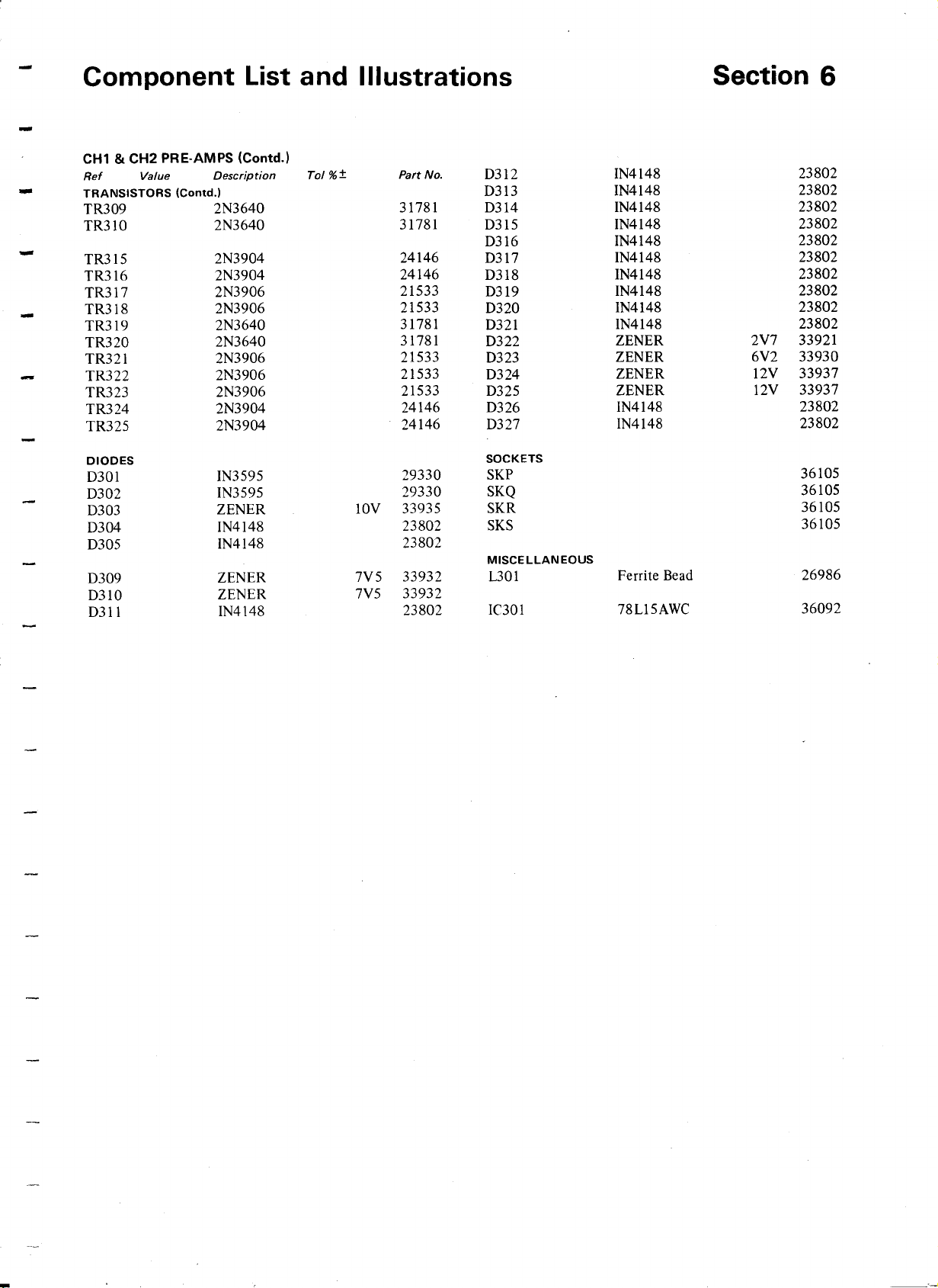
-
-
-
Component List and Illustrations
CH1 & CH2 PRE·AMPS (Contd.l
Ref
TRANSISTORS
TR309
TR310
TR315
TR316
TR317
TR318
TR319
TR320
TR321 2N3906
TR322
TR323 2N3906
TR324 2N3904
TR325 2N3904
Value Description Tal
(Contd.l
2N3640 31781
2N3640 31781
2N3904 24146
2N3904 24146
2N3906 21533
2N3906 21533
2N3640 31781
2N3640 31781
2N3906
%±
Part No.
0313 IN4148
21533
21533
21533
24146
24146
Section 6
0312 IN4148
0314 IN4148
0315 IN4148 23802
0316
0317 IN4148
D318 IN4148 23802
0319 IN4148
D320
D321
0322 ZENER
0323 ZENER
0324
0325 ZENER 12V 33937
0326 IN4148 23802
0327
IN4148 23802
IN4148
IN4148
2V7
6V2
ZENER
IN4148
12V 33937
23802
23802
23802
23802
23802
23802
23802
33921
33930
23802
DIODES
0301
0302
0303
0304
0305
0309
0310
0311
SOCKETS
IN3595
IN3595
ZENER 10V 33935 SKR 36105
IN4148 23802 SKS
IN4148 23802
ZENER 7V5 33932
ZENER 7V5 33932
IN4148 23802 IC301 78Ll5AWC
29330 SKP 36105
29330 SKQ 36105
36105
MISCELLANEOUS
UOl
Ferrite Bead
26986
36092
Page 59

-
-
-
Component List and Illustrations Section 6
ANALOGUE TO DIGITAL CONVERTOR
Ref Value Description
RESISTORS
R101
R102 390
R103
R104 1k2
R105 820
R106 1k
R107 47
10
10
CF
CF
CF
CF
CF
CP
MO
Tol
%±
Part No,
21793
28722 R163
21793
21800
28724
35875
26748
Ref
RESISTORS
R162 5k6
R170 470
R171 1k
Rl72
R173 1k
Value Description Tol
(Contd.)
CF
A.O.T.
CF
CF
1k
CF
CF
%±
Part No,
21806
21797
21799
21799
21799
R110 696R5
RIll
Rl12
Rl13 12k
Rl14
Rl15
Rl16
R120 12k
R121
R122 1k
R123
R124 220
R125
R126
Rl27 12k
R128 6k96
R129 47
R130 1k2
R131 12k
R132 R214
R133
R134
R135
R136
R137 27k8
R138 1k2
R139 8k9
R140 5k6
R141
R142 5k6
R143 47
R144 47
R145 47
R146 10
R147
R148
R149 10
R150 10
R151 10
R152
R156 47
R157 -
R158 47
R159 47
R160 5k6
R161 5k6
330
1k
6k8
1k2
1k2
13k5
1k
330
13k9
1k2
12k
5k6
10
10
10
47
MF
CF
CF
CP
MF
CF
CF
CF
CP
MF
CP
MF
CF
CF
MF
CF
CF
CF
MF
CF
CF
MF
CF
MF
CF
CF
CF
CF
CF
CF
MF
MF
MF
MF
MF
MF
MF
CF
CF
CF
CF
CF
CF
.25 35874
28721
21810
35875
35873
21800
21810
21800
35875 R204 3k9
35872 R205 2k7
35877
36032
28721
21810
35867
28714
21800
21810
35868 R214
21800
21810
35871
21800
35869
21806
21806
21806
28714
28714
28714
27314
27314
27314
27314
27314
27314
27314 R233 100
28714 R235
28714
28714
28714
21806 R240 1k
21806 R241 1k8
R181 2k2
R182
R183 2k2
R184 1k
R185 1k5
R186 220
R201 47
R202 3k9
R203
R206 4k7
R207 100
R208
R209
R210 560
R211 2k2
R212 1k
R213
R215 22
R216 22
R217 4k7
R218 6k8
R219 5k6
R220 3k9
R221 470
R222
R223 3k9
R224 10k
R225 3k9
R226 1k
R227
R228 22
R229
R230
R231 470
R232
R234 1k
R236 100
R237
R239 47
1k2
220
2k7
47
22
22
1k2
47
470
22
680
2k2
68
CF
CF
CF
CF
CF
CF
CF
CF
CF
CF
CF
CF
CF
CF
CF
CF
CF
CF
CF
CF
CF
CF
CF
CF
CF
CF
CF
CF
CF
CF
CF
CF
CF
CF
CF
CF
CF
CF
CF
CF
CF
CF
CF
CF
CF
CF
21802
21802
21799
21801
21796
28714
21804
21800
21804
28726
21805
21794
35881
28726
18547
21802
21799
28714
28710
28710
28710
28710
35879
21807
21806
21804
18546
21802
21804
21809
21804
21799
28714
28710
21797
28710
21797
28723
21794
21799
21802
21794
28716
28714
21799
28725
(
' ..f--··I ~-
, I-- --
"_ V /
\,-.1,.'.
~,\\l \
I-'
t,,'-,
v-
i
Page 60
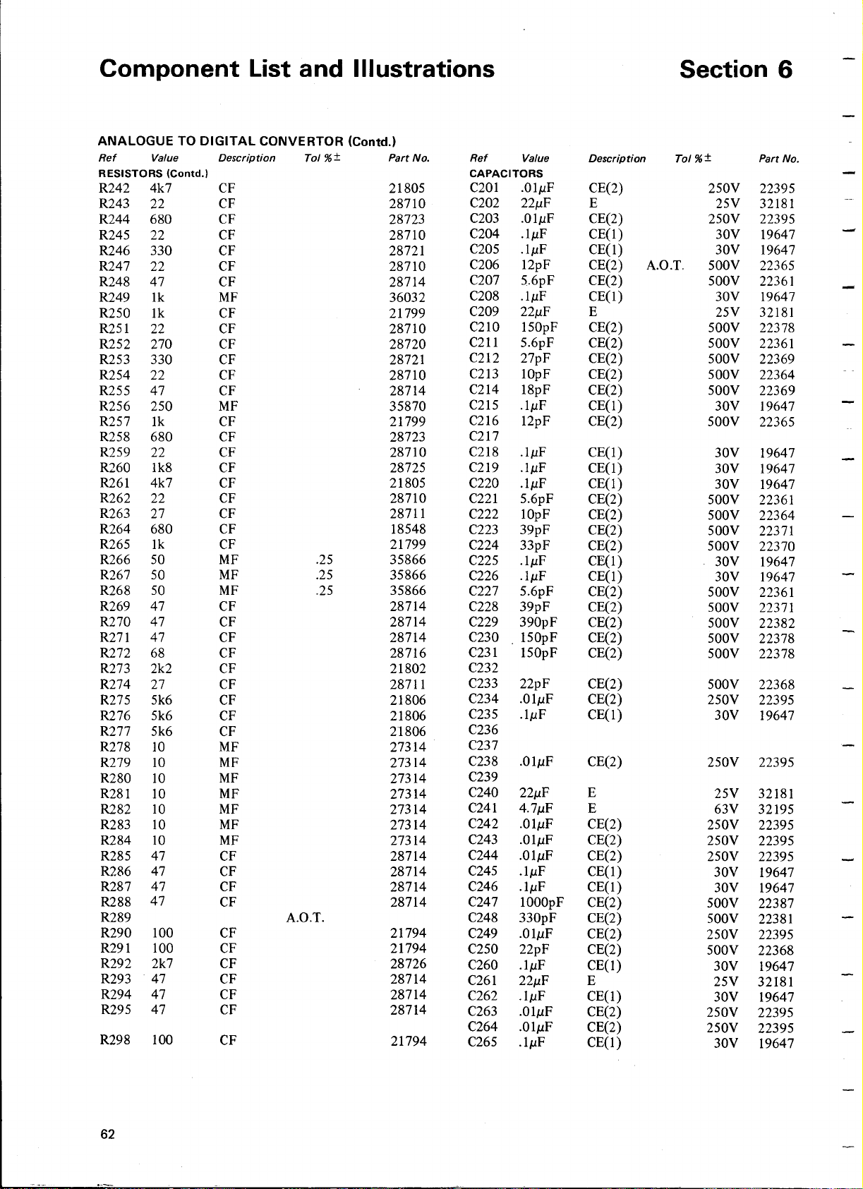
Component List and Illustrations
ANALOGUE TO DIGITAL CONVERTOR (Contd.)
Ref Value
RESISTORS
(Contd.)
R242 4k7 CF 21805
R243 22
R244 680
R245 22 CF 28710
R246 330 CF 28721
R247
R248
22
47 CF 28714
R249 lk MF
R250 lk CF
R251
22
R252 270 CF 28720
R253 330 CF 28721
R254 22 CF 28710
R255
47
R256 250 MF
R257 lk CF
R258 680 CF 28723
R259
22
R260 lk8 CF 28725 C219
R261
R262
R263
R264
4k7 CF 21805
22 CF 28710
27
680
R265 lk
R266 SO MF
R267 SO MF .25
R268 SO MF .25 35866
R269 47 CF 28714
R270 47 CF 28714
R271 47 CF
R272
68
R273 2k2 CF
R274
27 CF 28711
R275 5k6 CF 21806
R276 5k6 CF
R277 5k6
R278
R279
R280
10
10
10
R281 10
R282 10 MF
R283
10
R284 10 MF
R285 47 CF
R286 47
R287
R288
47
47
R289
R290
100
R291 100 CF
R292 2k7 CF 28726
R293 47 CF 28714
R294 47
R295 47
R298 100
Description
Tol
%±
Part No. Ref
CF 28710
CF
28723
CF 28710
36032
21799
CF 28710
CF
28714
35870
21799
CF 28710
CF
28711
CF 18548
CF 21799
.25
35866
35866
28714
CF
28716
21802
21806
CF 21806
MF 27314
MF 27314
MF
27314
MF 27314
27314
MF
27314
27314
28714
CF 28714
CF 28714
CF
A.Q.T.
CF
28714
21794 C249
21794
CF 28714
CF 28714
CF
21794
CAPACITORS
C201
C202
C203
C204
C205
C206 12pF
C207 5.6pF
C208
C209
C210
C211 5.6pF
C212
C213
C214 18pF
C215
C216
C217
C218
C220
C221 5.6pF
C222 lOpF
C223 39pF
C224 33pF
C225
C226
C227
C228
C229 390pF
C230
C231
C232
C233 22pF
C234
C235
C236
C237
C238
C239
C240
C241
C242
C243
C244
C245
C246
C247
C248
C250 22pF
C260
C261
C262
C263
C264
C265
Value
.011lF
221lF
.011lF
.IIlF
.IIlF
Description Tol
CE(2)
E
CE(2)
CE(l) 30V
CE(l)
CE(2)
CE(2) 500V 22361
.IIlF
22IlF
150pF
CE(l) 30V
E
CE(2)
CE(2) 500V 22361
27pF
lOpF
CE(2)
CE(2) 500V
CE(2) 500V
.IIlF
12pF
.IIlF
.IIlF
.IIlF
CE(l)
CE(2) 500V
CE(l)
CE(l)
CE(l)
CE(2)
CE(2)
CE(2) 500V
CE(2)
.IIlF
.IIlF
5.6pF
39pF
CE(l)
CE(l)
CE(2)
CE(2)
CE(2)
. 150pF
150pF
CE(2)
CE(2) 500V 22378
CE(2)
.011lF
.IIlF
.011lF
221lF
4.71lF
.011lF
.011lF
.011lF
.IIlF
.IIlF
1000pF
330pF
.011lF
CE(2) 250V
CE(l)
CE(2) 250V
E
E
CE(2) 250V
CE(2)
CE(2)
CE(l)
CE(l)
CE(2)
CE(2)
CE(2)
CE(2)
.IIlF
22IlF
.IIlF
CE(l)
E
CE(l)
.011lF CE(2)
.011lF
.IIlF
CE(2)
CE(l)
A.Q.T.
%±
250V
250V
25V
Part No.
22395
32181
22395
19647
30V 19647
500V 22365
19647
25V
32181
500V 22378
500V
22369
22364
22369
30V 19647
22365
30V
30V
30V
500V
500V
19647
19647
19647
22361
22364
22371
500V
22370
30V 19647
30V 19647
500V
500V
22361
22371
500V 22382
500V 22378
500V
22368
22395
30V
19647
22395
25V 32181
63V
32195
22395
250V
250V
30V
30V
500V
500V
250V
500V
30V
25V
22395
22395
19647
19647
22387
22381
22395
22368
19647
32181
30V 19647
250V
250V
22395
22395
30V 19647
Page 61
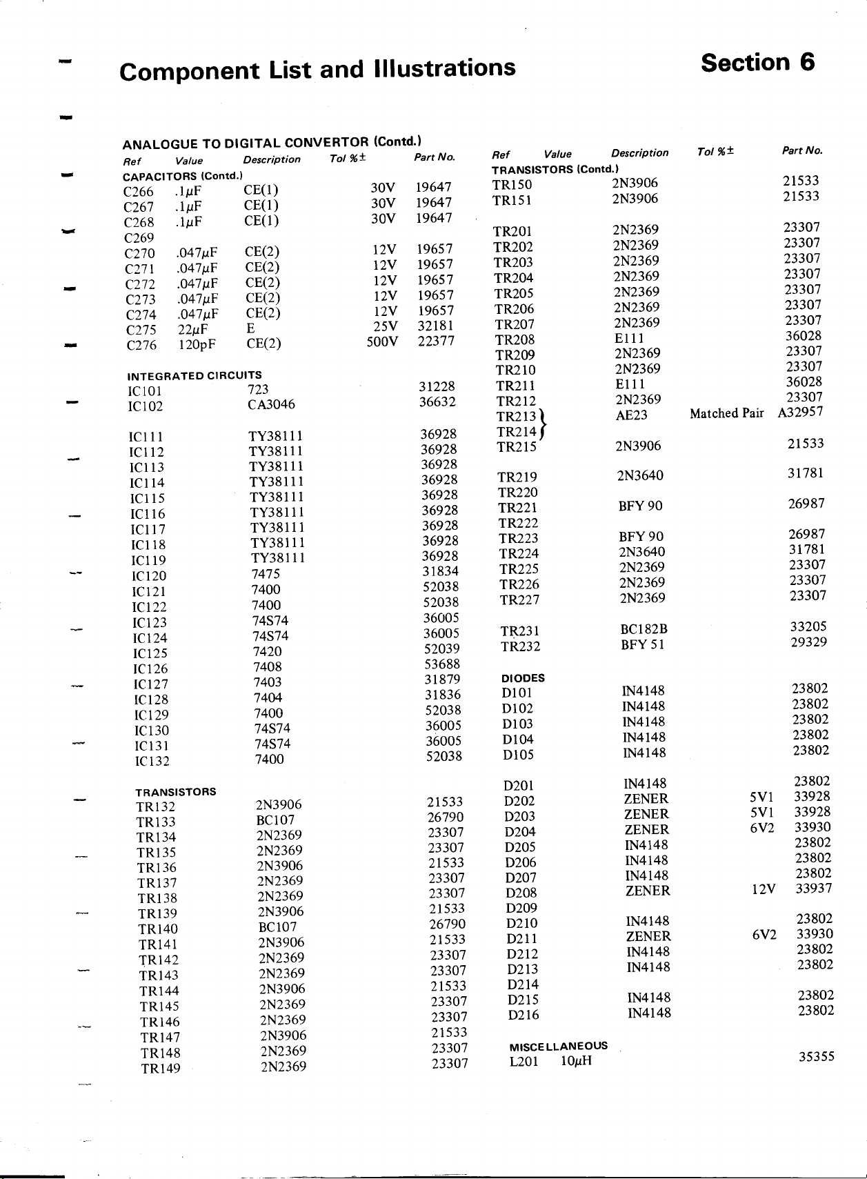
-
-
-
-
-
-
Component List and Illustrations
ANALOGUE TO DIGITAL CONVERTOR (Contd.l
Ref
CAPACITORS IContd.1
C266
C267
C268
C269
C270
C271
C272
C273
C274
C275
C276
INTEGRATED CIRCUITS
lCI0l
lCI02
lC 111
lC 112
lC 113
lC114
lC115
IC116
lC117
IC118
lC119
lC120 7475
lC 121
lC122
IC123 74S74
lC124 74S74
IC125
IC126
lCI27
lC128
lC129 7400
IC130
lC 131 74S74
lC132
Value
.IMF
.IMF
.IMF
.047MF
.047MF
.047MF
.047MF
.047MF CE(2)
22MF
120pF CE(2)
Description
CE(l)
CE(l)
CE(l)
CE(2)
CE(2)
CE(2)
CE(2)
E
723
CA3046
TY38111
TY38111
TY38111
TY381 11
TY38111
TY38111
TY38111
TY38111
TY38111
7400
7400
7420
7408
7403
7404
74S74
7400 52038 DI05
Tol
%±
30V 19647
30V 19647
30V 19647
12V
12V
12V
12V 19657 TR205
12V
25V
500V
Part No.
19657
19657
19657 TR204
19657 TR206
32181
22377
31228
36632
36928
36928
36928
36928
36928
36928
36928
36928
36928
31834
52038
52038
36005
36005
52039
53688
31879
31836
52038
36005
36005
Ref
TRANSISTORS IContd.1
TR150
TR151
TR201
TR202
TR203
TR207
TR208
TR209
TR210
TR211
TR212
TR213 }
TR214
TR215
TR219
TR220
TR221
TR222
TR223
TR224
TR225
TR226
TR227
TR231
TR232 BFY 51
DIODES
DI0l
DI02
DI03
DI04
Value
Section 6
Description
2N3906
2N3906
2N2369
2N2369
2N2369
2N2369
2N2369
2N2369
2N2369
El11
2N2369
2N2369
E11l
2N2369
AE23 Matched Pair
2N3906
2N3640
BFY90
BFY90
2N3640
2N2369
2N2369
2N2369
BC182B
IN4148
IN4148
IN4148
IN4148
IN4148
Tol
%±
Part No.
21533
21533
23307
23307
23307
23307
23307
23307
23307
36028
23307
23307
36028
23307
A32957
21533
31781
26987
26987
31781
23307
23307
23307
33205
29329
23802
23802
23802
23802
23802
TRANSISTORS
TR132
TR133
TR134
TR135
TR136
TR137 2N2369
TR138
TR139 2N3906
TR140 BC107
TR141
TR142 2N2369 23307
TR143
TR144
TR145
TR146
TR147
TR148
TR149
2N3906
BCI07
2N2369 23307
2N2369
2N3906
2N2369
2N3906
2N2369
2N3906
2N2369
2N2369
2N3906
2N2369
2N2369 23307
21533
26790
23307
21533
23307
23307
21533
26790
21533
23307
21533
23307
23307
21533
23307
D201
D202 ZENER
D203 ZENER
D204
D205
D206 IN4148
D207
D208
D209
D210
D211
D212 IN4148
D213
D214
D215 IN4148
D216
MISCELLANEOUS
L20l
IOMH 35355
IN4148
ZENER
IN4148
IN4148
ZENER
IN4148
ZENER
IN4148
IN4148
23802
5Vl
5Vl 33928
6V2
12V 33937
6V2 33930
33928
33930
23802
23802
23802
23802
23802
23802
23802
23802
Page 62
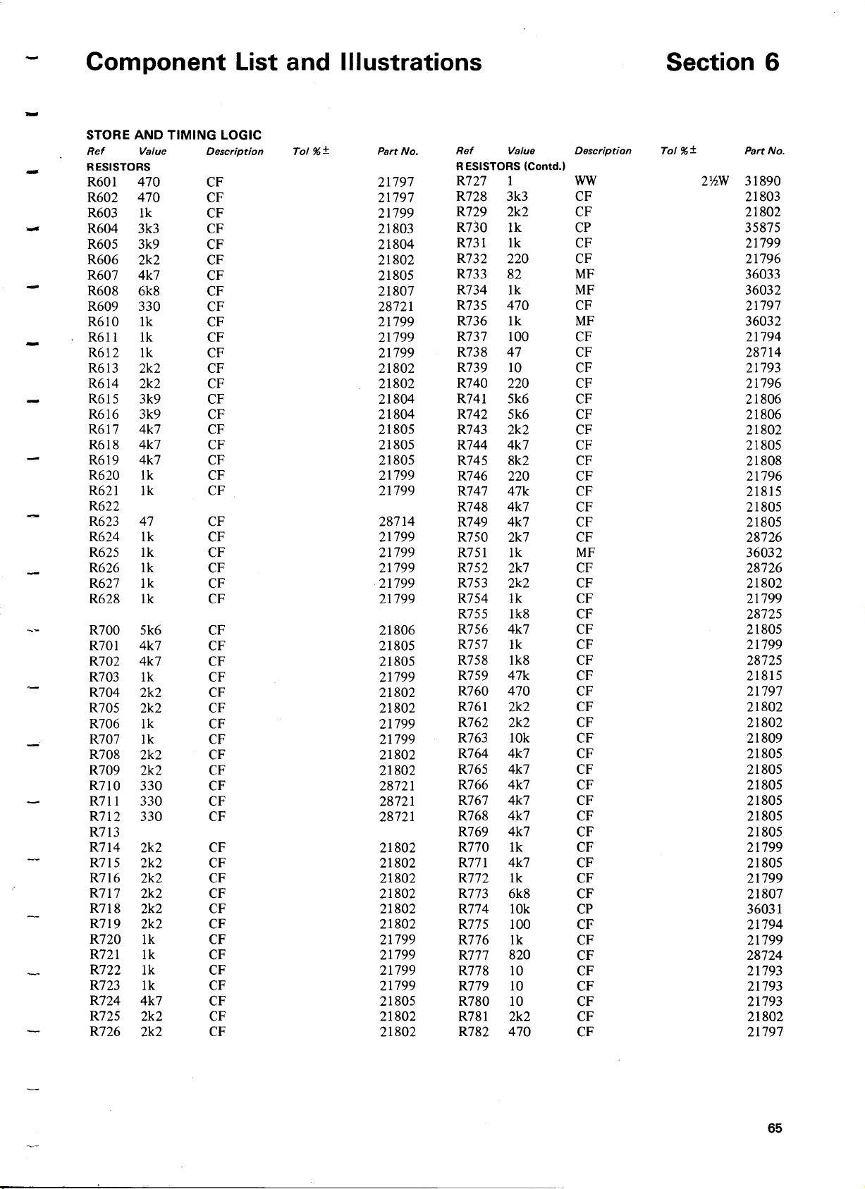
Component List and Illustrations
Section 6
-
-
-
-
STORE AND TIMING LOGIC
Ref Value
RESISTORS
R601 470
R602 470
R603
R604 3k3
R605 3k9
R606 2k2
R607 4k7
R608 6k8
R609 330
R610
R611 1k
R612
R613 2k2
R614
R615 3k9
R616 3k9
R617 4k7
R618
R619 4k7
R620 1k
R621
R622
R623 47
R624 1k
R625 1k
R626 1k
R627 1k
R628 1k
R700 5k6
R701 4k7
R702
R703 1k
R704 2k2
R705 2k2
R706
R707
R708 2k2
R709 2k2
R710
R711 330
R712 330
R713
R714
R715 2k2
R716 2k2
R717
R718 2k2
R719 2k2
R720
R721
R722
R723 1k
R724
R725 2k2
R726
1k
1k
1k
2k2
4k7
1k
4k7
1k
1k
330
2k2
2k2
1k
1k
1k
4k7
2k2
Description
CF
CF
CF
CF
CF
CF
CF
CF
CF
CF
CF
CF
CF
CF
CF
CF
CF
CF
CF
CF
CF
CF
CF
CF
CF
CF
CF
CF
CF
CF
CF
CF
CF
CF
CF
CF
CF
CF
CF
CF
CF
CF
CF
CF
CF
CF
CF
CF
CF
CF
CF
CF
CF
Tol
%±
Part No.
21797
21797
21799
21803
21804
21802
21805
21807
28721
21799
21799
21799
21802
21802
21804 R741 5k6
21804 R742
21805
21805
21805
21799
21799
28714
21799
21799
21799 R752 2k7
21799
21799
21806
21805
21805
21799
21802
21802
21799
21799
21802
21802
28721
28721
28721
21802
21802
21802
21802 R773
21802
21802
21799
21799
21799
21799
21805
21802 R781
21802 R782
Ref Value Description
RESISTORS (Contd.)
R727 1
R728 3k3
R729
R730 1k
R731 1k
R732
R733
R734
R735
R736 1k
R737
R738 47
R739 10
R740
R743 2k2
R744 4k7
R745 8k2
R746
R747
R748 4k7
R749 4k7
R750 2k7
R751 1k
R753 2k2
R754 1k
R755 1k8
R756 4k7
R757
R758 1k8
R759 47k
R760
R761 2k2
R762 2k2
R763 lOk
R764 4k7
R765 4k7
R766 4k7
R767 4k7
R768 4k7
R769 4k7
R770
R771
R772 1k
R774 10k
R775
R776 1k
R777 820
R778 10
R779 10
R780 10
2k2
220
82
1k
470
100
220
5k6
220
47k
lk
470
1k
4k7
6k8
100
2k2
470
WW
CF
CF
CP
CF
CF
MF
MF
CF
MF
CF
CF
CF
CF
CF
CF
CF
CF
CF
CF
CF
CF
CF
CF
MF
CF
CF
CF
CF
CF
CF
CF
CF
CF
CF
CF
CF
CF
CF
CF
CF
CF
CF
CF
CF
CF
CF
CP
CF
CF
CF
CF
CF
CF
CF
CF
Tol
%±
2YzW
Part No.
31890
21803
21802
35875
21799
21796
36033
36032
21797
36032
21794
28714
21793
21796
21806
21806
21802
21805
21808
21796
21815
21805
21805
28726
36032
28726
21802
21799
28725
21805
21799
28725
21815
21797
21802
21802
21809
21805
21805
21805
21805
21805
21805
21799
21805
21799
21807
36031
21794
21799
28724
21793
21793
21793
21802
21797
Page 63
Component List and Illustrations
STORE AND TIMING LOGIC (Contd.)
Ref
RESISTORS
R783
R784 330
R785
R786 2k2
R787
R788
R789 2M2
R790
R791 4k7
R792
R793
R794 1k
R795
R796 1k
R797
R798
R799 56
CAPACITORS
C601 15pF
C602
C603
C604
C605
C606
C607
C608 100pF CE(2)
C609
C610
C611
C612
C613
C614
C615
C616
C617
C618
C619
C620
C621
C622
C623
C624
C625
C626
C627 220pF
C628
C629
C701
C702 47pF
C703 680pF
C704
C705
C706 56pF
C707 220pF
Value Description
IContd.)
4k7
CF
CF
2k2
CP
CP
100 CF
180 CF
CC
2k2 CF
CF
1k
2k2
CF
CF
CF
560
CF
CF
1k8
1k8
CF
CF
MF
TRIMMER
22pF
.047,uF
.047,uF
.047,uF
.047,uF
.047,uF
.047,uF
.047,uF
.047,uF
.047,uF
.047,uF
.047,uF
.047,uF
.047,uF
lO,uF
CE(2) 34348
CE(l) 12V
CE(l)
CE(l)
CE(l)
CE(l)
CE(l)
CE(l)
CE(l)
CE(l)
CE(l)
CE(l)
CE(l) 12V
CE(l)
E
CE(2)
.l,uF
.01,uF
CE(l) 30V 19647
CE(2) 250V
CE(2)
CE(2) 500V 22385
1000pF
330pF
CE(2) 500V
CE(2) 500V 22381
CE(2)
CE(2) 500V
Tol
%±
Part No.
21805
28721
36030
3603.0
21794
21795
1180
21802
21805
21799
21802
21799
21798
21799
28725
28725
36034
36227
19657
12V 19657
12V
19657 C732
12V 19657 C733
500V
12V
12V
22376 C734
19657 C735
19657
12V 19657
12V 19657
12V
12V
19657
19657
12V 19657
19657
12V
25V
500V
19657
32180
22379
22395
250V 22372
22387
500V
22373
22379
Ref Value
CAPACITORS
C708
C709
C710 lOpF
C711
C712 3/lOpF TRIMMER
C713
C714 560pF
C715 560pF
C716 100pF
C717 220pF
C718
C719
C720
C721
C722
C723
C724
C725
C726
C727
C728
C729
C730
C731
C736
C737
C738·
C739
C740 1500pF
C741
C742
C743
INTEGRATED CIRCUITS
IC602
IC603
IC604
IC605
IC606
IC607
IC608
IC609
IC610
IC611 7404
IC612
IC613
IC614
IC615
IC616
IC617
IC618
IC619
(Contd.)
.1,uF
560pF
.1,uF
12/75pF
.01,uF
.01,uF
22,uF
.1,uF
.1,uF
.01,uF
22,uF
.047,uF
.047,uF
.047,uF
.047,uF
1,uF
.047,uF
.047,uF
.047,uF
.047,uF
.1,uF
.047,uF
.047,uF
100pF
.01,uF
.01,uF
Section 6
Description
CE(2) 30V
CE(2) 500V
CE(2) 500V 22364
CE(l) 30V
TRIMMER
CE(2)
CE(2)
CE(2) 500V
CE(2) 500V
CE(2) 250V
CE(2) 250V 22395
E
CE(l) 30V
CE(l)
CE(2)
E
CE(l)
CE(l) 12V
CE(l)
CE(l) 12V
PE
CE(l)
CE(l) 12V
CE(l)
CE(l) 12V
CE(l)
CE(l)
CE(l) 12V
CE(2)
CE(2)
CE(2) 250V
CE(2)
74874
7420
7400
7403
7400
74874
7475
8242 OR 9386
7400
7475
7475
Tol
%±
25V 32181
30V
250V 22395
25V 32181
12V 19657
12V
63V
12V
12V
30V
12V
500V 22376
500V 22388
250V 22395
Part No.
19647
22394
19647
32669
36091
36093
36093
22376
22379
22395
19647
19647
19657
19657
19657
31364
19657
19657
19657
19657
19647
19657
19657
22395
36005
52039
52038
31879
52038
36005
31836
31834
35679
52038
31834
31834
Page 64

Component List and Illustrations
Section 6
-
-
-
-
-
-
STORE AND TIMING LOGIC (Contd.)
Tol
Ref
INTEGRATED CIRCUITS
lC620
lC621
lC622
lC623
lC624 lC719
lC625
lC626
lC627
lC628
lC629
lC630
lC631 7482
lC632
lC633
lC634
lC635
lC636
lC637
lC638
lC639
lC640
lC641
lC642
lC643
lC644
lC645
lC646
lC647
lC648
lC650
lC651
lC652
lC653
lC654
lC655
lC656
lC657
lC658 TR702
lC659
lC701
lC702
lC703
lC704
lC705
lC706
lC707
lC708
lC709
lC710
lC711
lC712
lC713
lC714
Value
Description
(Contd.)
7476
7475
8242 OR 9386
8242 OR 9386
7400
4102-1 OR 2102-1
4102-1 OR 2102-1
7474
7400
7410
4102-1 OR 2102-1 35680
4102-1 OR 2102-1
4102-10R2102-1
7474
74157
8242 OR 9386
7476
7476
4102-1 OR 2102-1
4102-1 OR 2102-1
4102-1 OR 2102-1
7475
74157
8242 OR 9386
7493
7493
7495A
7475
74157
8242 OR 9386
7493
7493
7495A
7400
7400
7404
7400
7400
7476
7400
7403
MOSTEK 5009
7403
%±
Part No. Ref
INTEGRATED CIRCUITS
33448
31834
35679
35679
52038
35680
35680
52098
52038
35678
52043
35680
35680
52098
36007
35679
33448
33448 lC735
35680
35680
35680
31834
36007
35679
52341
52341
36006
31834
36007
35679
52341
52341
36006
52038
52038
31836
52038
52038
33448
52038
31879 TR714
34952 TR715
31879
lC715
lC716
lC717
lC718
lC720
lC721
lC722
lC723
lC724
lC725
lC726
lC727
lC728
lC729
lC730
lC731
lC732
lC733
lC734
lC736
lC739
lC740
lC741
lC742
lC743
lC744
lC745
TRANSISTORS
TR601
TR602
TR603
TR701
TR703
TR704
TR705
TR706
TR707
TR708
TR709
TR710
TR711
TR712
TR713
TR716
TR717
TR718
Value
Description
(Contd.)
7403
7410
7476
7400
7410
7476
7476
7476
7400
7476
7405
7400
7400
7400
7410
7400
7474
7403
7400
7476
7400
7476
7476
SL702C
702C
1408-8
2N2369
2N3640
2N3640
BC212
BCI08
BN2369
2N2369
El11
2N2369
2N2369
BC214C
BC212
El11
BC212
El11
2N2369
2N2369
2N2369
Tol
%±
Part No.
31879
52043
33448
52038
52043
33448
33448
33448
52038
33448
53637
52038
52038
52038
52043
52038
52098
31879
52038
33448
52038
33448
33448
30214
24789
35683
23307
31781
31781
29327
26110
23307
23307
36028
23307
23307
36019
29327
36028
29327
36028
23307
23307
23307
Page 65

Component List and Illustrations
STORE AND TIMING LOGIC (Contd.l
Ref
DIODES
D601
D602
D603
Value Description Tol
%±
Part No.
35202
35202
35202
Ref Value
SWITCHES
S601
S602
S603
Description
Section 6
Tol%±
Part No
35344
35343
35344
D701 6V2 ZENER
D702 IN4148
D703 11'V ZENER
D704
D705
D706
D707
D708
IN4148
IN4148
IN4148
IN4148
IN4148
D709 5V6 ZENER
D710 IN4148
D711 12V
D712
0713
ZENER
IN4148
IN4148
33930
23802
33936
23802
23802
23802
23802
23802
33929 SKB 36096
23802
33937
23802
23802
D714
D715
D719 IN4148 23802
DnO
Dnl
1701
6V2
33pH
IN4148
ZENER
23802
33930 SKM
33204
S701
S702
S703
S704
SOCKETS
SKA
35341
35341
35342
35342
36096
SKD 36096
SKE 36096
SKH 36096
SKJ 36096
SKK
SKL
36096
36096
36096
SKY
36105
Page 66

Component List and Illustrations
TIMEBASE
Ref
RESISTORS
R900
R901
R902
R903
R904
R905
R906
R907
R908
R909
R910
Value
47 CF
10 CF
390
lk2
lk2 CF
47 CF
15 CF
15 CF
3k3 CF
82 CF
10
R911
R912
R913
R914
R915
R916
R917
560 CF
220
220
560
2k2 CF
22k CF
R918 820k
R919
R920
R921
R922
R923
R924
R925
R926
330 CF
120 CF
270 CF
22k CF
22k CF
820k CF
330
lk8 CF
R927
R928
R929
270k CF
3k9 CF
R930 2k7 CF
R931
R932
R933
10 CF
220
lk5 CF
R934 3k3
R935
4k7 CF
R936 lk CF
R937
R938
10k CF
lk CF
R939 IM
R940 lk
R941
R942
R943
R944
22k
270 CF
3k3 CF
2k2 CF
R945 2k2
R946
R947
R948
2k2 CF
4k7 CF
56k
R949 82k
R950
R951
R952
R953
R954
R955
22k CF
12k CF
18k CF
3k9 CF
3k9 CF
47k CF
Description
Tol
%±
PartNo.
28714
21793
CF
CF
28722
21800
21800
28714
28708
28708
18556
28717
CF
21793
21798
CF
CF
CF
21796
21796
21798
21802 R972 4k7
21812
CF
32360
28721
28718
28720
21812
21812
32360 R980 3k9 CF
CF
28721 R981
28725
32356
21804
28726
21793
CF
21796
21801
CF
21803
21805
21799
21809
21799
CF
CF
CF
31840
21799
21812
28720
21803
21802
CF
21802
21802
21805
CF 28729
CF
21818 RI005 22k
21812
21810 RI007
21811 RI008 43k
21804 RI009
21804
21815
Ref Value Description
RESISTORS
R956 56k CF
R957
R958 lOOk CF
R9S9 12k CF
R960
R961
R962 6k8
R963
R964
R965
R966 2k2
R967
R968 2k2 CF
R969 2k2
R970
R971
R973
R974
R975
R976
R977 56k
R978 68k
R979
R982 56k CF
R983
R984
R985
R986 lk6
R987
R988
R989
R990
R991 120
R992
R993 10k
R994
R995 lk8 CF
R996 lk3 MO
R997
R998 lk8 CF
R999
RI000
RI00l
RI002 27k
RI003 22k
RI 004 4k7 CF
RI006
RIOI0 4k3
RIOll 2.5k
Section 6
Tol
%±
(Cont.)
lOOk CF
22k CF
CF
27k CF
lk2 CF
CF
2k2 CF
CF
27k CF
3k9 CF
CF
IOk CF A.O.T.
22k CF A.O.T.
2M2 CC
100 CF
CF
CF
100
100
CF
CF
lk8 CF
IOk WW
100 CF
MO
3k9 CF
10k PCP
180 CF
250 PCP
CF
100 CF
ww
56k CF
lk6 MO
100 CF
15k CF
15k CF
CF
CF
CF
27k CF
lOOk MF
MO
2.5k PCP
MO
PCP
lW 19058
lW
4W
4W 29481
lW
Part No.
28729
21819
21819
21810
21812
21807
21813
28100
21802
21802
21802
21802
21813
21804
21805
21809
21812
1180
21794
21816
21794
21804
21794
19058
28725
29481
21794
28793
21804
39265
21795
40355
28718
21794
19058
28725
28792
28793
28725
21794
28727
28727
21813
21812
21805
21812
21813
29476
26723
40354
26723
40354
Page 67

Component List and Illustrations
Section 6
-
-
TIMEBASE
Ref
RESISTORS (Cont.)
R1012 2.5k PCP
R1013
R1014
R1015 3k3 CF
R1016 4k7 CF
R1017 2.5k PCP
R1018 2k7
R1019 900
R1020
R1021 10k CF
R1022 1k CF
R1023 2k2 CF
R1024 10 CF
CAPACITORS
C901
C902 33pF CE(2)
C903 33pF CE(2)
C904
C905 27pF CE(2)
C906
C907
C908 470pF CE(2)
C909
C910
C911 270pF CE(2)
C912 .00~F
C913
C914 27pF CE(2)
C915 27pF CE(2)
.
C916 27pF
C917
C918
C919
C920 220pF CE(l)
C921
C922
C923
C924
C925
C926 27pF CE(2)
C927 1000pF CE(2)
C928 220pF CE(2)
DIODES
D900 IN4148
0901
D902 IN4148
D903 IN4148
D904
D905
D906 IN4148
D907 IN4148
D908 IN4148
D909
D910
(Cont.)
Value Description
CF
MF
100
.Q1~F
.01~F
.47~F
.47~F
4700pF
.01~F
.01~F
.01~F
0.047~F
.1~F
.1~F
.l~F
.01~F
.047~F
.01~F
8V2
MF
CE(2)
CE(2)
CE(2)
CE(2)
CE(2)
CE(2)
CE(2)
CE(2)
CE(2)
CE(2)
CE(2)
CE(2)
CE(2)
CE(2)
CE(2)
CE(2)
CE(2)
IN3595
IN4148
ZENER
IN4148
IN4148
Tal
%±
250V 22395
500V 22370
250V 22395
500V
3V 35352 TR903 2N2369
160V 31381 TR904
500V 22383
500V 22393
250V
500V 22380
250V 22395 TR909
250V 22395
500V 22369
500V 22369
500V 22369
250V 22395
30V 19647
30V 19647
30V 19647
1%
30V
250V 22395
500V 22369
500V 22387
500V 22379
Part No.
40354 0911
21803
21805
40354
28726
35582
35581
21809
21799
21802
21793
500V
22370
22369
22395
12V 19657
11587
24886
2793
23802
29330
23802
23802
23802
33933 TR933
23802
23802
23802
23802
23802
Ref
DIODES (Contd.)
D912
D913
0914
0915
D916
D917
D919
INTEGRATED CIRCUITS
IC901
IC902
IC903
IC904
IC905
IC906
TRANSISTORS
TR901 2N2369
TR902
TR905
TR906
TR907
TR908
TR910
TR911
TR912
TR913
TR914
TR915
TR916
TR917
TR918
TR919
TR920
TR921
TR922
TR923
TR924
TR925
TR926
TR927
TR928
TR929 MPF102
TR930
TR931
TR932
TR934
SWITCHES
S900
S901
Value Description
Tal
%±
IN4148
IN4148
IN4148
IN4148
ZENER
OA47
IN4148
7403
7400
7476
7403
7400
7410
2N2369
2N2369
BC212
BC182B
BC212
2N2369
2N2369
BC21'2
2N2369
2N2369
2N2369
BC108
2N2369
2N2369
BC108
2N2369
2N2369
2N2369
BC212B 36900
BC212
BC182B
BC212
BF258
BF258
BC212
MPF102
2N2369
2N2369
BC212
BC212 29327
BC212
5V6
Part No.
23802
23802
23802
23802
33929
35202
4468
23802
31879
52038
33448
31879
52038
52043
23307
23307
23307
23307
29327
33205
29327
23307
23307
29327
23307
23307
23307
26110
23307
23307
26110
23307
23307
23307
29327
' 33205
29327
31490
31490
29327
25870
25870
23307
23307
29327
29327
35999
35343
Page 68

-
-
-
-
-
Component List and Illustrations
INTERCONNECTIONS
Ref Value Description Tol
RESISTORS
RI 22k CP
R2 22k CP A4/35986
R3 470 CP
R4 470 CP
R5
R6 5k CP PartofS6
R7 22k
R8 lk+lk
R22 22 CF
R23 22
R24 990k
R25 22 CF 28710
R26 470k CC
R27 IM MF 26346
R28 18 CF
R29 16k MF
R30 15k8 MF
R31 5k23 MF
R32
R33 787 MF 3328& SI A3/31292
R34 360 MF
R35
R42
R43 22 CF
R44 990k
R45
R46
R47 IM
R48
R49 16k MF
R50 15k8 MF 33291
R51
R52 lk72 MF
R53 787 MF 33288
R54
R55
R57
R58 68k
R59
R90 lOOk CF lW 19061
R91
Rn
R93/98 RESISTOR NETWORK A3/36455
lk72
22
27
470k CC 10
18 CF 28709
5k23 MF 33290
360
270
150k
470 CF
4k7 CF 21805
CP With S7 A4/35338
CP R8a+R8b A4/36069
CF
MF
MF 33289
CF 28710
MF
CF 28711
MF
MF 33287
CF
CF
CF
%±
With S13 A4/36070
With S14 A4/36070
~
Y4W
~
Y4W
Part No.
A4/35986
28710
28710
31927
4906
28709 BR53 W04
29361
33291
33290
33287
28710
31927
4906
26346
29361
33289
28720
21816
21821
21797
Ref
CAPACITORS IContd.)
C45
C51 47
C90
C91
C92
C93
C94
C95
C96
RECTIFIERS
BR51 W04
BR52 W04
BR54 W04
BR55
SWITCHES
S2
S3 35998
S4
SS
S6 With R6 35345
S7
S13
S14 Partof R4
S51
S52 29057
DIODES
D53 IN4003
D54 IN4003
090 OA47
D91
SOCKETS
SKY
SKW
SKX
SKZ
Value
.001lF
0001l
5600pF
4.71lF
.0471lF
11lF
.011lF
6/25pF TRIMMER
47pF
Description
CE(2)
E
F
CE(2)
E
CE(2) 30V 2793
CE(2)
PE
CE(2)
VH148
OA47
Section 6
Tol
%±
500V 24902
10V 36024
500V 22394
63V 32195
63V
160V
Partof R7
PartofR3
Part No.
24888
24886
23593
685
29367
29367
29367
29367
36281
A3/31292
35998
A4/36232
32771
32771
4468
4468
1222
1222
1222
24913
CAPACITORS
C20
C25
C40
.11lF
.011lF
.11lF
PE
CE(2)
PE
400V
500V
400V
29495
24902
29495
MISCELLANEOUS
L20
L21
L22
L23
L24
L25
FX1242 26986
FX1242 26986
FX1242
FX1242 26986
FX1242 26986
FX1242 26986
26986
 Loading...