

Page 1
054001
OUTPUT UNIT
Instruction Manual
-} GOULD ADVANCE
Telephone 01-5001000
Telegrams Attenuate Ilford
Telex 263785
Page 2
SECTION 1
SECTION 2
SECTION
SECTION
Introduction
Specification
Operating Instructions
3
General
3.1
Chart recorder speed
3.2
Driving a chart recorder 5
3.3
The Read-out cycle 5
3.4
Remote start
3.5
Function Generation
3.6
3.7 Digital Outputs
Circuit Description
4
4.1 General
D-A Converter
4.2
Latches and latch control 9
4.3
4.4
X-ramp counter 9
4.5 Data Selector
4.6 Clock delay
10
3
SECTION 5
4
5
Maintenance
Fitting the 4001 to the OS4000
5.1
5.2 Access
Fault finding
5.3
Setting up Procedure
5.4
12
12
13
14
15
5
5
SECTION
Circuit Diagrams and Components
6
Schedules 17
5
SECTION
7
7
8
8
9
Fig. 1
Fig. 2
Fig. 3 Block diagram
Fig. 4
Fig. 5
9
Fig. 6
Fig. 7
Fig. 8
Guarantee and Service Facilities
7
ILLUSTRATIONS
Typical read-out cycle
Connections to back panel socket
Data Selector - mechanical
equivalent
Clock delay - timing diagram
Internal view of 4001
Fixing details
Circuit diagram
21
6
7
8
10
11
12
13
19
Page 3
Introduction
The 400 I option is designed to be added to a standard
OS4000 Digital Storage Oscilloscope to enable the infor-
mation in store to be retransmitted in both analogue and
digital form. Two analogue outputs are provided, and
these are intended primarily to drive strip chart and X-V
recorders. Channel I and 2 signals are available simultan-
eously at a read-out rate which can be varied to suit the
chart recorder, with a slowest time of 200 seconds
representing the 10 division display. In addition, a
corresponding X-ramp signal is provided for X-Y recorder
use. The unit also incorporates relay contacts for pen lift
or chart motor control. There is a variable delay between
the closing of these contacts and the start of read out
which can be preset to allow a chart drive motor to
accelerate.
.A socket on the rear panel presents the output infor-
mation in digital form as two eight bit parallel signals for
Y and one ten bit parallel signal for the X ramp. Control
facilities for remote start and continuous readout are also
provided. The latter can be used for continuous
generation of a recorded transient or frequency shift of
recorded waveforms.
Page 4
Specification
Section 2
ANALOGUE OUTPUTS Via B.N.C. connectors
Channels 1 and 2
Amplitude lOOmV per cm of screen height.
Bipolar with OV corresponding to
middle of screen
Accuracy Output voltage per cm of display±3%
Output to input voltage (ca!)
X Ramp
Amplitude
Time output accuracy of Y Channel outputs±1%
(Record to replay ratio)
Output Impedance CHI, CH2 and X-ramp
DIGITAL OUTPUTS Via back panel socket
Channels I and 2
X Ramp
Accuracy
lOOmV per cm of screen width.
Positive ramp resetting to OV
Output voltage/cm of display±J%
Output voltage/unit time recorded±3%
100H/0.IJ.lF
Continuous short circuit protected
All outputs true binary from open
collector T.T.L. buffers
8 bit parallel, negative logic
10 bit parallel, negative logic
Y Channel full scale=9cm of display±5%
X Ramp full scale=II.3cm of display ± 5%
±
3%
Remote continuous read-out by T.T.L. low or contact
closure to ground.
Delay between start command and
initiation of read-out cycle set by front
panel preset control from <20msec to
> I sec.
(lOJ.lsec. to lOsec. by internal component
change)
Front panel access via 4mm sockets to
isolated single pole contact which closes
from start command to end of read-out
cycle
Contact rating 200V D.C. 0.5 A D.C.
IOWD.C. Isolation 400V max.
OUTPUTS
Oocks I and 2
Negative T.T.L. pulses, 100nsec.
duration marking the change of
each digital word.
T.T.L. low, commencing at the end
of delay, for the duration of the
read-out cycle.
READ OUT RATE
Set on OS4000 time base range switch
Range 20sec/cm to
Read-out bandwidth D.C. - 16kHz (-3dB)
CONTROLS
Front panel start button to initiate single read-out cycle.
Remote start by T.T.L.low or contact closure to ground.
200J.ls/cm
DIMENSIONS 3.75cm extra height to OS4000
WEIGHT 570gm extra (l
ACCESSORIES 36 way plug Ampheno157-30360
%
Ib) to OS4000 approx.
2 x 4mm plugs
Handbook PN 36896
Page 5
Operation
3.1
ANALOGUE OUTPUTS
The 4001 may be used to drive strip-chart, T-Y or X-V
recorders. Both Y channels are available simultaneously
for chart recorders with two pens. Alternatively, the two
channels may be reproduced sequentially on single pen
recorders. A synchronised X-ramp is available to drive
X-V recorders as Y-t. Alternatively, the CHI and CH2
outputs can drive an X-Y display directly.
The internal contacts can be used to control chart motor
and/or pen lift if required.
3.2
CHART RECORDER SPEED
The 4001 offers a very wide range of read-out rates to suit
the recorder being used. The rate should be chosen by
considering the following:
1) A slow read-out rate, while faithfully reproducing
the stored signal, will also show the discrete levels
in the output waveform, (there is no dot-joining on
the 4001 outputs). A faster read-out rate and chart
recorder speed will tend to smooth the output wave·
form.
2) If too high a read-out rate is chosen, the chart
recorder may be unable to follow any large ampli-
tude fast change of the signal. This is slew-rate
limitation of the recorder.
The optimum read out speed for any particular
stored waveform is thus the maximum at which the
chart recorder is capable of tracking the signal. This
may be determined by increasing the readout/chart
recorder speed each sweep until waveform degrad-
ation can be observed.
The bandwidth of the output amplifier is d.c. to
16kHz (-3d B) which is well above the limitation of
most chart recorders. However this limitation may
be reached if the output is required for other
purposes when the replay frequency is a function
of recorded waveform and replay rate.
(See Function Generator)
3.3
DRIVING A CHART RECORDER
1) Connect to the CHI, CH2 and X-ramp sockets as
reqUired. In single trace operation, the same signal
will be present at CHI and CH2 outputs.
Set the sensitivity of the chart recorder inputs to
accommodate±400rn V f.s. on CHI and CH2 and
o
to 1V on the X-ramp.
When the 4001 is not reading out, the CHI and 2
and the X-ramp outputs return to
V-channel output corresponds to mid-screen on the
OS4000 display and thus the chart recorder pen
should be set to mid-scale unless specifically
required otherwise.
The X-ramp moves positive fromOVand thus the
OV.
Ov on the
pen should be positioned to allow at least 1V
positive travel.
2) Connect, if required for remote start/pen lift.
NOTE: The relay contacts are unprotected and
inductive loads should be suppressed to stay within
the contact rating.
3) The delay time (from closing of relay contacts to
start of read-out) is set by a front panel screwdriver
preset. The minimum delay time of < 20rns is
sufficiently short for recorders for which no delay
is required. The preset control range allows the
delay time to be set to a maximum of 1 second but
this can be increased to approx. 10 sec. by increasing
the internal capacitor C80I to I5tlF.
4) Obtain the required trace on the OS4000 and
STORE or LOCK it. If the 50% hold facility is
being used, the trace stored by the 50% hold will
appear at the CH2 output, the other trace appearing
at CHI.
5) Set the required read-out rate on the timebase range
switch.
6) Press the start switch to initiate the read-out cycle.
Note the display is inhibited during read-out. At
slow read-out rates, this will result in a blank screen
for considerable periods. Similarly the OS4000 is
prevented from accepting new data into the store
during this period.
7) At the end of the read-out cycle, reset the timebase
range switch as required to record subsequent data.
3.4
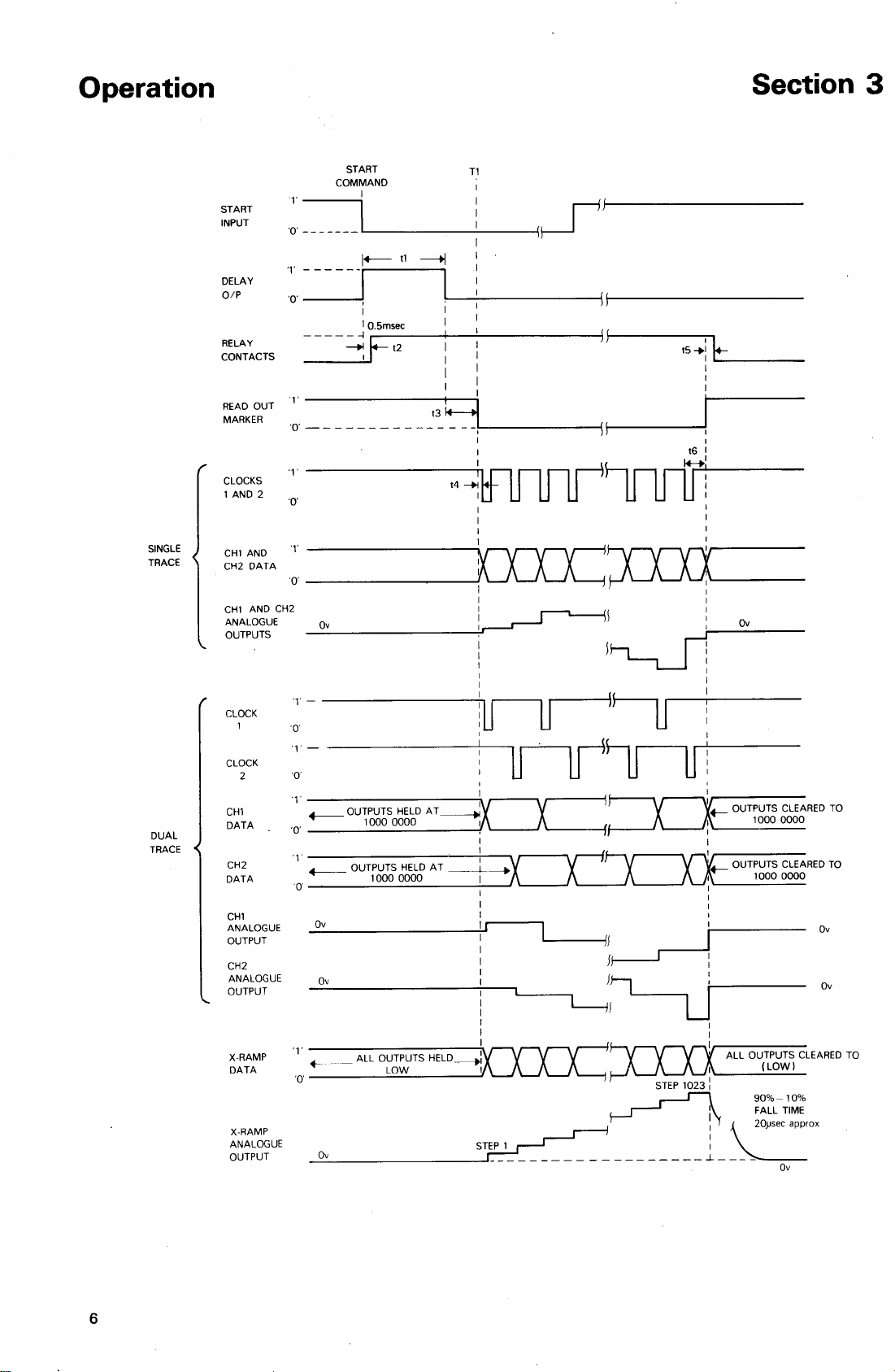
THE READ-OUT CYCLE
Fig. 1 shows a typical read-out cycle. The cycle is
initiated by a negative edge on the start input produced
by the push button or by remote start (see section 3.5).
The relay contacts close within 0.5msec. of the start
command and the preset delay period is started. At the
end of this delay, the read-out is primed to start at T1
the end of the current display sweep on the 0S4000.
Period t3 has any value from 0 to I.2msec. depending
on when the button was pushed but is unlikely to be a
significant delay at chart recorder speeds. If required,
the read-out marker, available at the back panel socket
SK A.C. pin 2, can be connected to the chart recorder
event marker to indicate the exact start of read-out. At
the end of read-out, the relay contacts open again within
0.5ms and all analogue outputs return to
3.5
REMOTE START
The remote start input appears on contact 3 on the back
panel socket SK AC. Read-outs may be initiated by a
T.T.L.low on this contact or by connecting it to contact
4 which is logic earth. This action has the identical effect
to pushing the front panel button.
OV.
Page 6
Operation
DELAY
OIP
START
COMMAND
,~:--------j-----<\~:
1__
11
----.j
',~,------I
I I
10.5msec I
----~Ft2
1--------<\1----1 ----
i
I
I
I
I I
Section 3
SINGLE
TRACE
CLOCKS
1 AND 2
CHl AND
CH2 DATA
CHl AND CH2
ANALOGUE
OUTPUTS
CH'
ANALOGUE
OUTPUT
CH2
ANALOGUE
OUTPUT
X-RAMP
ANALOGUE
OUTPUT
'~', -- -- _I~
'0'
'1'
'0'
Dv
...-- OUTPUTS HELD AT --------.: .- OUTPUTS CLEARED TO
'" ID;:
'0' 1000 0000 '. . _
". I I
..---- OUTPUTS HELD AT
_Ov II- ----
'1'
f- __
'0' LOW i~~ (LOW)
1000 0000 I
ALL OUTPUTS HELD---,~r-y-y--y-y ALL OUTPUTS CLEARED TO
9~---------<\1-----
I
,
I
14 -+I
I
I
I
,
I
I
: Qv
j~
iUlJ
lJlr~
I
, I
l~
---1-----. ~
I I
I :
I
: :1
I
I
i
I I
I
STEP'
___________________ ..L _
J~
~Ir-,
STEP 1023 :
~
I
I
I
I
I
I
r---
I
LJ
I
i
: ~o}Jsec
I
1000 0000
OUTPUTS CLEARED TO
1000 0000
90%-10%
FALL TIME
approx
Dv
Dv
Page 7

Operation
3.6 FUNCTION GENERATION
Although primarily intended to be used to drive chart
recorders, the analogue outputs can be used for other
applications. In the continuous run mode, the 4001 acts
as a function generator, continuously repeating the one or
two waveforms stored.
Thus a single transient can be recorded at one speed and
regenerated continuously at another faster or slower
speed, within the available stepped range of timebase
sweep speeds. (20 sec/cm to 200~s/cm.) As the scan
length is approx. 11.5 cm, this range is equivalent to 230
seconds to 2.3ms for a full cycle. For example a slow
stimulus into a servo system could be recorded and
replayed faster for analysis in an electrical analogue of
the servo.
Alternatively functions can be "written" manually on the
screen of the OS4000 by use of the shift control or
externally controlled input during a very slow scan in the
refreshed mode.
Such a single scan can be started by operation of the
trigger level control and frozen at any point by the 'Lock
Store' button. The latter is necessary at some point
during a scan for operation of the X shift control so that
the end of scan can be brought on screen. When the
'Lock Store' button is released the scan continues from
the point at which it was frozen. To write a second trace
in this mode, the Lock Alt. Samples button should be
pressed and the writing process repeated. The two
patterns will be generated simultaneously from the CHI
and CH2 outputs. Such outputs could be used for XY
display on another oscilloscope or chart recorder.
Continuous readout is obtained by shorting Pin 1 on the
rear panel socket to Pin 4 (ground).
3.7
DIGITAL OUTPUTS
The chart in Fig.2 shows the'digital outputs and controll-
ing inputs available at back panet socket SKAC. These
outputs come from open collector T.T.L. buffers without
pull-up resistors.
Fig.l shows a typical read-out cycle. The read-out cycle
is initiated by a negative edge on the start input, which
triggers the delay period t1. This delay may be set in the
range 20ms to 1 sec. by the front panel control or if
required it can be reduced to less than 50~sec.by changing
C801 to 1000pF.
Read-out will commence at Tl, the end of the current
display sweep on the OS4000. Thus there will be a period
t3, after the end of the initial delay, of 0 to 1.2msec.
approx. according to the relative timing of the start
command and the OS4000 sweep before the read-out is
enabled.
There will be a further delay, t4, between the read-out
enable and the first clock pulse, where t4 is dependent
upon the read-out rate chosen. For a read-out rate of
N sec./cm, t4 will be in the range 0 to N x 11 X
10-3sec,
Section 3
Th~ problems due to the uncertainty of these delays are
reduced (or removed) by clocks 1 and 2, whose negative
edges indicate when the data is updated in channels 1 and
2 respectively. These clocks may be used to latch the
data at the receiving digital equipment.
CHI data is shown as changing first when in dual channel
operation. This is only in the case when the 084000 is in
the 'Refreshed' mode. In the 'Roll' mode, each sweep
does not start at the beginning of store (see 0S4000
handbook). This results in an uncertainty as to which
channel output will appear first. Again, recourse should
be made to clocks 1 and 2.
Pin No.
1
2
3
4
5
6
7
8
9
10
11
12
13
14
15
16
17
18
19
20
21
22
23
24
25
26
27
28
29
30
31
32
33
34
35
36
Connection
Continuous read-out input
Read-out marker
Remote start input
Logic earth (OV)
Clock 1
Clock 2
Dl (Most Significant)
D2
D3
D4
D5
D6
D7
D8
D9
DlO (Least significant)
Not connected
Not connected
Dl (Most significant)
D2
D3
D4
D5
D6
D7
D8 (Least significant)
D1 (Most significant)
D2
D3
D4
D5
D6
D7
D8 (Least significant)
Not connected
Not connected
Page 8

Circuit Description
4.1 GENERAL
Fig.8 shows the full circuit detail0f the 4001.
References of components on the P.C.B. are in the range
800 to 899.
Components in the range 80 to 89 are on the front panel
of the 4001.
Interconnection between the 0S4000 and the 4001 is
obtained by breaking the direct links SKK to SKD and
SKA to SKH in the OS4000 and reconnecting SKA to
SKAA, SKD to SKDD etc. (see Fig.26 of 0S4000 hand-
book). This provides access to the Y-Channel data and
permits 0S4000 control signals to be modified by the
4001.
+
5V WRITE
RELAY RATE
x::::::::::=:
GATE
&
DELAY
Section 4
PULSES
BUFFERS
[>0
START BUTION ~
.l
READ-OUT WRITE
ENABLE RATE
B-BIT DATA
\ IN
In essence, operation of the start button initiates the
delay period. At the end of this period the control
circuitry is primed to start a read-out at the end of the
current display sweep of the OS4000. During read-out,
the clock to the OS4000 read address counter is changed
to the slower rate determined by the timebase range
switch. At the end of the slow read-out scan, the control
circuit is reset and the OS4000 returns to normal
operation.
(a) CH1 and CH2
Y channel data is obtained from the OS4000 in the form
of an 8 bit word as read out from the stores.
Consider the circuit when operating in dual trace mode.
Channel 1 information is contained in odd store locations
and Channel 2 information in even locations. In order to
PULSES
j
BUFFERS
[>0
1
separate the two channels and present them simultan-
eously, the incoming data is held in two sets oflatches,
one clocked on even addresses, the other on odd. The
latched information is then passed on to the digital to
analogue converters (D to A) and also to the buffers,
which protect the internal data from external effects
such as short circuits or line reflections. At the end of
read-out, the latches are cleared to binary 1000,0000
which produces
(b) X Ramp
The X-ramp is produced digitally by a 10 bit counter
clocked at each change of data input. The counter is
cleared to all zeros at the end of read-out. The output of
this counter feeds a third D to A and is buffered as is the
Y data for the digital output.
av
(mid range) at the analogue outputs.
CHl
OUT
CH2
OUT
Page 9

Circuit Description
(c)
Timing
The start of read-out is initiated by triggering the delay.
This immediately energises the relay. At the end of the
delay period, the start latch is set, holding the relay and
putting a '1' on the D of the enable latch. The next
sweep reset from the OS4000 clocks this' l' to the out-
put and enables the read-out.
The start latch is cleared after two clock pulses putting a
'0' on the D of the enable latch. The relay is now held on
by theQof the enable latch. When the next 'sweep reset'
pulse arrives at the end of the slow scan, this '0' is clocked
to the output and the read-out enable goes low clearing
the Y channel latches and resetting the X-ramp, thus
terminating read-out.
The NORM input inhibits read-out when the OS4000 is in
the normal mode, by putting a '0' on the D input of the
start latch and on the clear input of the enable latch.
4.2 D/A CONVERTERS
The D/ A converters, IC821, 822, 823, are similar to those
used in the OS4000. The output current produced at
Pin 4 is converted into an output voltage by the following
operational amplifiers, IC 824, 825, 826. The current
injected into Pin 14 of the D to A defines the output
scaling, and the external current injected into Pin 4 of the
D to A, sets the zero. Each has a preset control to com-
pensate for component tolerances. Both pins are virtual
earth points and so the currents can be completely
defined by a reference voltage and a series resistor. The
reference voltage is provided by regulator, IC827. The
resistor and capacitor on the output remove any high
frequency pick up. Each channel has a half scale offset
current introduced by R848, 849 and R841, 842 such
that mid-screen on the display produces OV out.
The X-ramp operates on 10 bits. The least significant
eight are converted to an analogue current by IC821.
The two most significant bits are generated separately for
current summation at the input of IC824.
These additional binary weighted currents are provided
by R822, R823 and R824 representing bit Dl, and R832,
R833 and R834 representing bit D2.
Transistors, TR802 and TR803, when switched on,
reverse bias diodes, D807 and D805/D806 respectively,
diverting the current from the summing junction. D804
is included in series with R854 to ensure thermal tracking
between the current from IC821 and the two additional
currents. IC821 draws a current toward -6V from the
summing junction, proportional to the digital input.
Correspondingly the two additional currents are normally
on when their digital inputs are zero and their total
current is balanced by that through R825 and R827.
R824 and R834 adjust the currents representing D2 and
Dl respectively. R829 adjusts the overall scaling without
changing the matching between the three currents.
4,3
LATCHES AND LATCH CONTROL
Refer to the circuit diagram, Fig.8.
The incoming data stream enters two 4-bit latches in each
Channel, IC819, 815 and IC814, 818. TheQoutputs are
used for all but the most significant bit, which arrives
inverted by IC804 (d) and is taken out from theQoutput.
This ensures that at the end of read-out when the clear is
taken low and all the latches cleared, the digital infor-
mation presented to the D/A is binary 1000,0000 which
is half full scale (OV at the analogue output).
IC807 gates the clock pulses such that:-
(a) In dual trace or 'Lock alternate samples' mode,
information from odd and even locations is clocked into
CHI and CH2 latches respectively.
(b) Information from all store locations is clocked into
both channels when in single trace operation.
The operation is as follows:-
The signal arriving at Pins 13 and 2 of IC807 is the clock
to be gated. The signal arriving at Pins 5 and 9 is the read-
out enable. When low it inhibits clocks to both latches
and clears them. When high, it enables clocks.
The input 'dual trace' is inverted by IC802 (b). In single
trace operation it puts a '0' on IC805 Pins 13 and 9 which
in turn puts a '1' on IC807 Pins 12 and 1. This allows
clocks to reach both Y Channel latches simultaneously,
fulfilling condition (b) above.
In dual trace operation or 'lock alt. samples', IC802 Pin 4
is high, enabling the read address LSB to arrive at IC807
Pin 1 and its inverse at Pin 12. Thus when the LSB is
High, the CHI latches receive clocks, when it is low CH2
receive clocks. This fulfils conditions (a).
4.4 X
IC817 and IC820 are each four bit synchronous binary
counters and with IC816 are cascaded to form a 10 bit
divider. They are cleared to zero at the end of each sweep
and stepped with each change of Y Channel data, Le.
following the read address through the read-out cycle.
4.5
Switches shown with '0' on select.
The data selector, IC808 functions as 4 changeover
switches as shown in FigA.
The OS4000 normally reads out from the stores at a fixed
RAMP COUNTER
DATA SELECTOR
Page 10

Circuit Description
rate. Switch (a) changes this rate to one set by the Time-
base switch, i.e. the write-rate pulses. The flip-flop,
IC805 (a) and (b), retimes the write-rate pulses from P2
to PI to drive the read address counter. (See Fig.5.)
In dual trace operation, the OS4000 normally reads even
store locations only on one sweep and odd only on the
next. (See section 4.5.4 of 0S4000 handbook.)
In the read-out mode, switch (c) ensures that the LSB
address is taken from Cl rather than Cl', retaining read-
out from all the store location. Switch (b) sends logic '0'
to the dot-joiner gating circuitry of the OS4000 in place
of Cl during read-out, while (d) sends logic to the read/
write control to inhibit writing into store.
4.6
CLOCK DELAY
Fig.5 shows the retimed write rate pulses which arrive at
IC803 Pin 3. These are sent to step the read address
counter but there is an inherent delay within the OS400C
before the data changes. Because of this delay of data it
is necessary to delay the start of clock pulses to the X-
ramp counter and to the Y-Channellatches by three P4
pulses.
The write-rate pulses are entered at the serial i.!l.Putof the
shift register, IC812, and clocked through by P4. Using
the output from the third stage of the register produces
the required delay. At the end of read-out, the shift
register is cleared to zero by parallel loading.
Page 11

Circuit Description
T
ORIGINAL READ
COUNTER PULSE
'0'
t
WRITE RATE PULSE
SLOW READ
COUNTER PULSE
IC808
pin
3
1ST STAGE CLOCK
DELAY
READ STORE
ADDRESS
DATA FROM STORE
P4
TJl
'0'
TJ
'Q'
T
0'
0
T
'Q'
T
'0
t
n
X
n
~
n
n n
r1
Fig.
NEW DATA
AT
alP
LATCH
2ND STAGE CLOCK
DELAY
3RD STAGE CLOCK
DELAY
IC812
pin
11
CLOCK TO RAMP
COUNTER
LA TCH GA TING
X DATA alP
5
Clock Delay - Timing Diagram
&
T
'0
T
'0'
T
'0'
T
'Q'
'1'
'Q'
~
U
~
Page 12

Section 5
5.1 FITTING THE 4001 TO THE 084000
The 4001 kit to be fitted to an OS4000 comprises:
Part Number
1 4001 assembly
2 Cable and plug assy 'A'
2 Cable and plug assy 'B'
4 Nut special
4 Pillar clamping
10 Washer 4-40 'Wavey'
1 Cover Bottom
6 Screws 4-40 x ~" Pan Head
A3/36892
A3/36893
A4/36827
A4/36826
4591
A2/36823
22694
Taptite
Fitting procedure
(1) Disconnect the OS4000 from the supply and
stand it on the back cover.
(2) Remove both covers of the OS4000, plus 4 feet.
(3) Unplug the ribbon cables connecting SKA to
SKH and SKK to SKD and plug in the four
ribbon cables supplied to each of the above
sockets as shown in Figs. 6 and 7b. (Long cables to
sockets A and H, short to K and D.) It is possible
to achieve this without removing the store and
timing logic boards, but if any difficulty is
encountered refer to the OS4000 handbook
section 5.2.2 to remove these boards.
(4) Place the special nuts on the OS4000 frame
extrusion, with the threaded hole inside as shown
in Fig.7a.
(5) Place the 4001 chassis in position and insert the
threaded pillars.
(6) Connect the power supplies as shown in Fig.7c.
The connectors are a push fit onto the supply pins.
(7) Plug in the four ribbon cables to the sockets on the
4001, connecting
SK A to SK AA
SK D to SK DD
SK H to SK HH
SK K to SK KK
POWER SUPPLY
CONNECTIONS
(SEE F;g 7)
DELAY
TIMING
COMPONENTS
C80l
• CHASSIS FIXINGS
• BOARD FIXING SCREWS
R 825
X ZERO
R 829
X CAL
Page 13

(8) The 4001 is now ready for setting up as detailed in
section 5.4. It should not be necessary to make any
adjustment to the OS4000.
(9) Fit the bottom cover to the 4001 with the ventil-
ation holes at the rear. The original bottom cover
of the OS4000 is not required when the 4001 is
fitted.
(l0) Fit 4 feet to the 4001.
4001
BACK/FRONT
PANEL
5;2 ACCESS
Access to the 4001 is obtained by unscrewing the six
retaining screws and removing the bottom cover. Fig.6
shows the location of the preset controls and test points.
Access to both sides of the board and to the preset
controls in the OS4000 may be obtained in the following
manner.
(l) Unplug PLC and PLG.
(2) Remove the three screws marked (.) in Fig.6.
The board is now free to hinge about the central bar.
OUTPUT UNIT
4001
,
.-
OS 4000
STORE LOGIC
BOARD
METHOD FOR CONNECTING
CABLES DD AND AA
TIMING LOGIC
BOARD
STORE LOGIC
BOARD
METHOD FOR CONNECTING
CABLES HH AND KK
TIMING LOGIC
BOARD
Page 14

+170V
Section E
+20V
~ b
GREY
5.3 FAULT FINDING
(a) All voltage measured with respect to OV as in Table 1
Supply
+5.V +4.8 to +5.2V Pin 1 with respect to
+12V
-6V
6.2V ref. 5.9 to 6.5V
With the exception of the 6.2V reference, the supplies are
derived from the 084000. If any disagreement with
Table 1 is encountered, disconnect the supplies at Pins 1,
2 and 11, 12 and 13 and check the incoming supplies. If
the fault lies with the main frame, refer to section 5 of
the OS4000 manual.
(b)
logic Levels
le's with the exception of IC's 802, 809, 810, 811, 813.
Logic '1', 2 to 4.5V
Logic '0', 0.15 to 0.7V
1C's 802, 809, 810, 811, 813 have open collector outputs
which require a pull-up resistor to +5V to attain the levels
indicated above.
(c) Fault Location
The following guide assumes that there is no fault in the
0S4000. This can be checked by by-passing the 4001
completely as follows:-
Measured
Voltage
11.5 to 12.5V Pin 12 w.r.t. Pin 13
5.75 to 6.25V
~!
BOTTOM EDGE
Location
Pin 2
Pin 11 w.r.t. Pin 13
Wiper of R834 w.r.t.
Pin 13
(a) Disconnect the four ribbon cables between the
4001 and the OS4000.
(b) Use two of these cables to connect SK A
directly to SK Hand SK K directly to SK D.
First check the supplies, then set the delay period to
maximum.
The following chart offers guidance on fault localisation;-
(i)
Digital read-out
but one or more
analogue outputs
inoperative.
(ii)
No read-out cycle
(OS4000 display
not interrupted)
but the L.E.D.
comes on for the
delay period.
(iii) L.E.D. perman-
ently on, no SKDD/KK Pin 1.
0S4000 display.
(1) +12V and -6V supplies.
(2) D/ A convertors.
(3) Operational Amplifiers.
(1) Sweep reset pulse on
SKDD/KK Pin 16 and
1C806 Pin 11.
(2) Clear inputs of
IC808.
(1) P4 clock pulses on
(2) Write rate pulses
(related to timebase
switch setting) on in-
put Pin 3 and output
Pin 4 of IC808.
(3) Check clocks to ramp
counter and ensure
count. Read-out
cannot terminate
untilQofIC816 (b)
clears IC806 (a).
Page 15

(iv) Both CH1 and
CH2 outputs
chopping between
CHI and CH2
signals at approx.
100 cycles per
displayed cm.
(v) Discontinuities in
the X-ramp.
SETTING UP PROCEDURE
Test Equipment
1. Calibrated dual trace oscilloscope.
2. Square wave generator.
Channels 1 and 2
Set the square-wave generator to 1kHz and the
0S4000 to CHI, 0.2ms/div. X expansion Xl.
Adjust the generator frequency and amplitude
display an 8 div peak to peak waveform with two
cycles occupying 10 div. Press "Full Store Lock".
Connect the 4001 CHI output to an oscilloscope
via the front panel BNC connector. Set the OS4000
timebase switch to 2ms/div. Connect TPl or its
remote on SK AC Pin 3, to logic earth to produce a
continuous read-out. Adjust R846 to produce an
800mV pk-pk output. Remove the earth on TPl
(1) SKDD/KK Pin 3 is
LO in dual trace
mode.
(1) Data bits missing.
(2) Mis-match between
IC821 current and
additional currents
see 5Ad.
and adjust R849 to produce OV d.c. out. Connect
the oscilloscope to the CH2 output and repeat
adjusting R839 and R842.
X-ramp
With the same stored display as in 5A(b) connect
an oscilloscope to the X-ramp output. Earth TPl
to produce continuous read-out. Connect the
second channel of the oscilloscope to the Channel
1 output. One cycle of the stored square wave,
representing 5 Div. of displayed trace, should also
correspond to 500m V of X ramp. Adjust R829 to
this effect.
Remove the earth on TPl and adjust R825 to
produce OV d.c. out.
X-ramp current matching
If any discontinuity is visible at the 14and/or72and
%
way points of the ramp, this means that the two
additional currents are no longer matched to the
current from IC821.
On one channel of an oscilloscope, display the
X-ramp in continuous read-out as in 5A(c).
Connect the other channel to R812.
R824 should be used to remove any step at the
quarter way point (coincident with the first positive
edge of D2) expanding the trace to view it if
possible. Adjust R834 to remove any step at the
half way point (negative edge of D2). When these
two are correctly adjusted there should be no
discontinuity at the three-quarter way point
(coincident with the second positive edge ofD2).
Repeat (c) above.
Page 16

Component List and Illustrations
ABBREVIATIONS USED FOR COMPONENT DESCRIPTIONS
Section 6
RESISTORS
CC
Carbon Composition
CF Carbon Film
MO Metal Oxide
MF
WW
CP
Metal Film
Wire Wound
Control Potentiometer
PeP Preset Potentiometer
CAPACITORS
CE(l)
CE(2)
SM
PF
Ceramic
Ceramic
Silver Mica
Plastic Film
PS Polystyrene
PE Polyester
Pe Polycarbonate
E
T
Electrolytic (aluminium)
Tantalum
1/
W
2
l/
W
S
1/
W
2
1/4W
6W
500V
10%
5%
2%
1%
5%
20%
20%
+
80%
- 25%
±
10%
10%
±
±
10%
+
50%
-
10%
+
50%
-
10%
unless otherwise stated
unless otherwise stated
unless otherwise stated
unless otherwise stated
unless otherwise stated
unless otherwise stated
unless otherwise stated
unless otherwise stated
unless otherwise stated
unless otherwise stated
Page 17

Component List and Illustrations Section 6
OUTPUT UNIT 4001
Ref Value DescriPtion Tol
RESISTORS
%±
Part No.
R81 1M CP A4/37898
R801 6k8 CF 21807
R802 4k7 CF
R803 lOk
R804
1M CF
R805 lOk
R806
4k7
CF
CF
CF 21805
R807 4k7 CF
R808
R809 4k7
470 CF
CF 21805
21805
21809
31840
21809
21805
21797
R810
R811 4k7
R812
8k2 CF
R813 8k2
R814
10
R815 2k7
R816 3k3
R817
10 CF
R818 3k3
R819
10 CF 21793
R820 3k3
R821
10
R822 180 CF
R823
3k MO
R824 220 PCP
R825 220 PCP
R826
R827
4k7
lkl
CF
21805 C809 lOnF
21808 C810
CF
CF
21808 C811 lOnF
21793
CF 28726
CF
21803
21793
CF
CF
CF
21803
21803
21793
21795
26727
35881
35881
CF
MO
21805
28791
R828 120 CF 28718
R829 100 PCP
R830
R831 2k7
100 CF
CF
R832 100 CF
R833
1k5 MO
R834 100 PCP
R835 680 CF
R836
R837
R838
R839
560 CF
560 CF
100 CF
lk CP
R840 3k3 CF
R841
R842
R843
R844
R845
R846
R847
6k8 CF
2k2 PCP
560
CF 21798
560 CF
100 CF
lk
3k3
PCP
CF
R848 6k8 CF
R849
2k2 PCP
36958
21794
28726
21794
26733
36958
28723
21798
21798
21794
35880
21803
21807
36868
21798
21794
35880
21803
21807
36868
R850.
R851
R852 4k7
R853
180 CF
R854 3k3
CF
MO
21805
21795
26726
Ref Value Description Tol
CAPACITORS
C81
.C82
C83
C801
C802
C803 lOnF
C804
C805 lOnF
C806
C807 1nF
C808 lOnF
.1J.lF
.1J.lF
.1J.lF
1.5J.lF
.68J.lF
2n2F
lOnF
CE(2)
CE(2)
CE(2)
PE
E 63V
CE(2) 250V 22395
CE(2)
CE(2) 250V 22395
CE(2)
CE(2) 500V 22387
CE(2) 250V 22395
CE(2) 250V 22395
33J.lF
E 16V
CE(2) 250V
C812
C813 lOnF
C814 lOnF
C815
C816 lOnF
C817
C818 lOnF
C819 lOnF
C820 100nF
C821 100nF
C822 100nF
INTEGRATED CIRCUITS
IC801
IC802'
IC803
IC804
IC805
IC806
33J.lF
10nF
lOnF
E 16V 32173
CE(2)
CE(2)
CE(2)
CE(2) 250V 22395
CE(2)
CE(2)
CE(2)
CE(2)
CE(2) 36709
CE(2)
555V
74LS05
74LSlO
74LS04
74LSOO
74LS74
IC807 74LSOO
IC808
IC809
IC810
IC811
IC812
IC813
IC814
IC815
IC816
IC817
IC818
IC819
IC820
IC821
IC822
IC823
IC824
IC825
IC826
IC827
74S157
74LS05
74LS05
74LS05
74LS95 36734
74LS05
74LS175
74LS175
74LS76
74LS161 36727
74LS175
74LS175
74LS161
1408-8
1408-8
1408-8
741
741
741
78L06
%±
Part No.
25V 36709
25V 36709
25V 36709
63V 31365
500V 22389
250V 22395
250V 22395
250V 22395
250V 22395
250V 22395
250V 22395
250V 22395
36813
36879
36867
36731
36730
36732
36730
36735
36879
36879
36879
36879
36728
36728
36733
36728
36728
36727
35683
35683
35683
36736
36736
36736
36959
32162
32173
22395
36709
36709
Page 18

Component List and Illustrations
OUTPUT UNIT 4001 (Contd.l
Ref
TRANSISTORS
Value
TR801
TR802
TR803
Description Tol%±
BC182B
2N2369
2N2369
Part No. Ref
33205
23307
23307
Value
MISCELLANEOUS
S81
RL801
Description
REED RELAY
Section 6
Tol
%±
Part No.
A4/35341
26755
DIODES
D81
D801
D802
D803
D804
D805
D806
D807
D808
L.E.D. TIL209A
IN4148
IN4148
IN4148
IN4148
IN4148
IN4148
IN4148
35202
23802
23802
23802
23802
23802
23802
23802
SKAC
SKAD
SKAE
SKAF
SKAG
SKAH
Ampheno157-40360
27513
26587
26587
26587
36946
36946
Page 19

Guarantee and Service Facilities
Section 7
This instrument is guaranteed for a period of two years
from its delivery to the purchaser, covering faulty work-
manship and replacement of defective parts other than
cathode ray tubes and batteries (where fitted). Cathode
ray tubes are subject to the manufacturers guarantee.
This assumes fair wear and tear and usage in the specified
environment and does not cover routine recalibrations
and mechanical adjustments.
Wemaintain comprehensive after sales facilities and the
instrument should be returned to our factory for servicing
if this is necessary. The type and serial number of the
instrument should always be quoted, together with full
details of any fault and service required.
Equipment returned for servicing must be adequately
Service Dept.,
Roebuck Road,
Hainault,
Essex,
IG63UE
Tel: 01-500 1000
Telex: 263785
Telegrams: Attenuate Ilford
packed, preferably in the box in which the instrument
was supplied and shipped with transportation charges
prepaid. We accept no responsibility for instruments
arriving damaged. Should the cause of failure during the
guarantee period be due to misuse or abuse of the instru-
ment, or if the guarantee has expired the repair will be
put in hand without delay and charged unless other
instructions are received.
Our Sales, Service and Engineering Departments are ready
to assist you at all times.
The Service Department can provide maintenance and
repair information by telephone or letter, if required.
Note: Please check fuses before returning instruments
for service.
 Loading...