

Page 1

http://www.
goepel.com
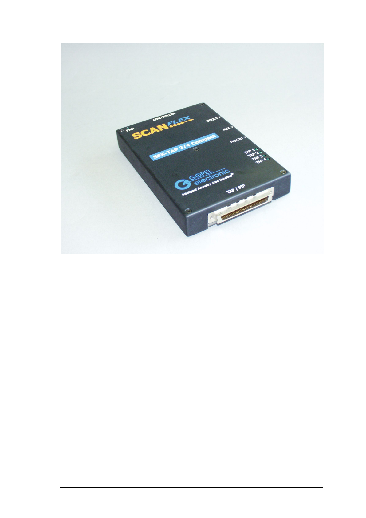
Desktop Transceiver
SFX-TAP4/C
SFX-TAP2/C
Technical Description
Version 0.1
Intelligent Boundary Scan Solutions®
GÖPEL electronic GmbH
Göschwitzer Str. 58/60
D-07745 Jena
Tel.: +49-3641-6896-0
Fax: +49-3641-6896-44
E-Mail: support@goepel.com
Page 2

© 2005 GOEPEL electronic GmbH. All rights reserved.
The software described in this manual as well as the manual itself are supplied under
license and may be used or copied only in accordance with the terms of the license.
The customer may make one copy of the software for safety purposes.
The content of the manual is subject to change without notice and is supplied for
information only.
In case of inaccuracies or errors appearing in this manual,
GOEPEL electronic GmbH assumes no liability or responsibility.
Without the prior written permission of GOEPEL electronic GmbH, no part of this
documentation may be transmitted, reproduced or stored in a retrieval system in
any form or by any means as well as translated into other languages (except as
permitted by the license).
printed: 02.08.2005
Rev.: 07/05
Author: Dietmar Beltz
Page 3

Table of Contents
1 Definition ........................................................................................................................ 5
1.1 Versions of the Desktop Transceiver...................................................................... 5
1.2 Scope of Delivery.................................................................................................... 6
2 Technical Data ............................................................................................................... 6
2.1 General Information ................................................................................................ 6
2.2 Dimensions ............................................................................................................. 6
2.3 Characteristics ........................................................................................................ 6
2.4 ESD / Latch up Strength ......................................................................................... 7
2.5 Current Input ........................................................................................................... 7
3 Device Structure............................................................................................................. 7
3.1 Interfaces ................................................................................................................ 7
3.2 Structure of the Desktop Transceivers SFX-TAP4/C (SFX-TAP2/C) ..................... 7
3.3 AUX Connector ....................................................................................................... 8
3.4 PwrCtrl Connector .................................................................................................. 8
3.5 TAP/PIP Connector ................................................................................................ 8
4 Hardware Components .................................................................................................. 9
4.1 Voltage Supply........................................................................................................ 9
4.2 PIP Complex ........................................................................................................... 9
4.3 Analog IO Signals ................................................................................................... 9
4.4 Digital IO Signals .................................................................................................... 9
4.5 Trigger Signals...................................................................................................... 10
4.6 Output Voltages .................................................................................................... 11
4.6.1 Output Voltages on TAP/PIP Connector: ...................................................... 11
4.6.2 Switch for the function of the PwrCtrl Connector:.......................................... 11
4.7 Boundary Scan Interface ...................................................................................... 12
4.8 Output Driver......................................................................................................... 12
4.8.1 Absolute Maximum Ratings........................................................................... 12
4.8.2 Recommended Operating Conditions ........................................................... 13
4.8.3 Electrical Characteristics ............................................................................... 13
4.9 Input Stage............................................................................................................ 15
5 Software Settings of the Testbus Interface.................................................................. 15
5.1 TCK Frequency..................................................................................................... 15
5.2 TAP Specific Settings ........................................................................................... 17
5.2.1 TIC Type........................................................................................................ 21
5.2.2 Output Voltage............................................................................................... 21
5.2.3 Input Voltage ................................................................................................. 21
5.2.4 Inline Resistor................................................................................................ 22
5.2.5 Pull Down Resistor ........................................................................................ 22
5.2.6 Power Relays ................................................................................................ 22
5.2.7 ADYCS II™.................................................................................................... 22
5.2.8 Testbus Signals on TAP/PIP User Interface ................................................. 25
5.2.9 SCP Controller............................................................................................... 25
6 Appendix ...................................................................................................................... 26
6.1 TAP/PIP : User Interface SFX-TAP4/C ................................................................ 26
6.2 TAP/PIP : User Interface SFX-TAP2/C ................................................................ 27
7 Order Information ......................................................................................................... 28
8 References................................................................................................................... 28
Desktop Transceiver SFX-TAP4_2/C, V0.1, Technical Description 3
Page 4

Page 5
1 Definition
The Desktop Transceiver SFX-TAP4/C (SFX-TAP2/C) is a Hardware product of the company
GÖPEL electronic GmbH and belongs to the product group Boundary Scan test tools. It can
only be operated together with the „SYSTEM CASCON“ and „POLARIS“ [1] software or a
respective dynamic link library (DLL) of version 4.2.1 or higher from GÖPEL electronic.
The SFX-TAP4/C (SFX-TAP2/C) is a Desktop Transceiver. In combination Host Controller
connected via a SFX cable, it forms a highly flexible Boundary Scan test system with:
• 4 (2) independent voltage and impedance programmable TAP’s
• ADYCS™ (Active Delay Compensation)
• Fast In System Programming (ISP)
• 32 Bit PIP (Parallel Interface Port)
• Trigger Signals (C-Bus)
• SCP-TAP on SFX-TAP2/C
• 2 analog I/O
• 4 (2) Power outputs, relay-connectable
1.1 Versions of the Desktop Transceiver
There are two versions available. Despite of their identical body structure, the performance is
different:
- Desktop Transceiver SFX-TAP2/C --> Compact Transceiver with 2TAP and one SCP-TAP
- Desktop Transceiver SFX-TAP4/C --> Compact Transceiver with 4TAP
Desktop Transceiver SFX-TAP4_2/C, V0.1, Technical Description 5
Page 6

1.2 Scope of Delivery
• SFX-TAP2/C or SFX-TAP4/C
• Power supply 5.0 V / 2.4 A
• SFX Cable
• this manual
2 Technical Data
2.1 General Information
The Desktop Transceiver SFX-TAP4/C (SFX-TAP2/C) forms together with the Host Controller a
Boundary Test System that allows versatile kind of connections the Unit-Under-Test (UUTs).
The following device properties allow maximum flexibility of the interface to the UUT:
• voltage-programmable Testbus interface in the range of 1.8V-4.5V, inputs (TDI
signals) in the range of 0V-3.0V
• 3-array impedance programming of the Testbus interface
• ADYCS™ (Active Delay Compensation)
• voltage-programmable 32 Bit Parallel Interface Port (PIP) in the range of 1.8V- 4.5V
• relay output (5V) or a logic signal at each TAP(2 or 4) on connector PwrCtrl for UUT
power control
• 2 analog I/O with 10 Bit resolution, (AD and DA converter on 2 pins of the AUX
connector)
• 3 digital I/O on AUX connector
• SFX/LS interface
• Trigger lines (2 output, 1 input) on AUX and on TAP/PIP connector
• SCP-TAP on SFX-TAP2/C
2.2 Dimensions
The Desktop Transceiver SFX-TAP4/C (SFX-TAP2/C) has following dimensions:
(L x W x H) 152 mm x 102.5 x 22 mm
2.3 Characteristics
Symbol Name Min. Typical Max. Unit
VDD Operating Voltage 4.75 5.0 5.25 V
T
Storage temperature -40 125 °C
stg
Ta Operating temperature 0 35 °C
6 Desktop Transceiver SFX-TAP4_2/C, V0.1, Technical Description
Relative storage humidity, not
condensing
Relative operating humidity,
not condensing
10 90 %
20 85 %
Page 7
2.4 ESD / Latch up Strength
All pins of the output drivers have an ESD strength of >1500V and a Latch up Strength of ±100
mA.
2.5 Current Input
The quiescent current is 700 mA.
The current input during operation depends on output driver loads, clock frequency as well as
the load of the power supply pins at connector.
3 Device Structure
3.1 Interfaces
Controller interface
SFX/LS interface
Testbus IEEE 1149.1 : TAP/PIP connector (68-pole, SCSI)
Parallel I/O interface : TAP/PIP connector (68-pole, SCSI)
C-Bus interface : TAP/PIP connector (68-pole, SCSI)
2 analog I/O : AUX connector
PowerCtrl OUT : PwrCtrl connector
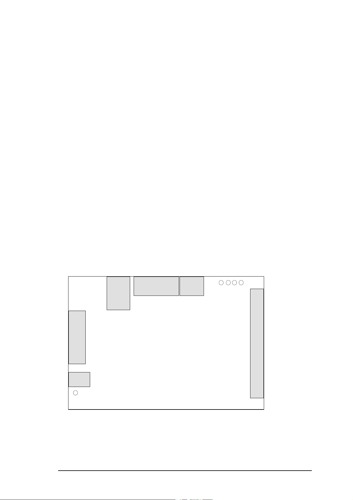
3.2 Structure of the Desktop Transceivers SFX-TAP4/C (SFX-TAP2/C)
AUX
SFX/LS
Controller
PWR
Figure 1: Assignment of the Connector and LED of the Desktop Transceiver SFX-TAP4/C (SFX-TAP2/C)
PwrCtrl
TAP1
TAP2
TAP3
TAP4
TAP/PIP
Desktop Transceiver SFX-TAP4_2/C, V0.1, Technical Description 7
Page 8
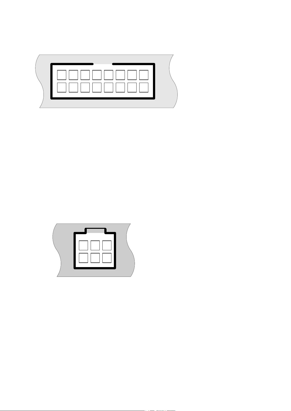
3.3 AUX Connector
35 171113 915
46 281214 1016
Figure 2: AUX connector on the side panel of the Compact Transceiver
Assignment of the AUX connector:
1 TRG0
3 TRG1
5 TRG2
7 D-AUX1
9 D-AUX2
11 D-AUX3
13 A-AUX1
15 A-AUX2
2, 4, 6, 8, 10, 12, 14, 16 GND
3.4 PwrCtrl Connector
35 1
46 2
Figure 3: PwrCtrl connector on the Side panel of the Compact Transceiver
Assignment of the PwrCtrl connector:
1 PWR1
2 PWR2
3 PWR3
4 PWR4
5 GND
6 GND
3.5 TAP/PIP Connector
For assignment see Appendix TAP/PIP – User Interface
8 Desktop Transceiver SFX-TAP4_2/C, V0.1, Technical Description
Page 9
4 Hardware Components
4.1 Voltage Supply
Die voltage supply of the Desktop Transceiver SFX-TAP4/C (SFX-TAP2/C) is obtained by using
the wall power supply. Connect it to the PWR plug of the Transceiver.
4.2 PIP Complex
Count of I/O: 32
Formatting: 4 x 8, 2 x 16
Input voltage range: 0 V – 5,0 V
Output voltage range: 1.8 – 4.5 V
For the PIP unit, there are no handshake signals available. The user must ensure a safe data
transmission.
The output driver of the PIP‘s are activatable group-wise which means 8 or 16 Bit each can be
in tristate or active mode.
The PIP complex is designed with the same driver circuitries as for TAPs. For further
information refer to chapter 4.8 and [2].
4.3 Analog IO Signals
Analog signals can be provided ore measured on pin 13 and 15 of the AUX connector. Signal
generation and Measuring are based on 10-bit converter technique. The voltage range covers 0
and 4.096 V with a maximum rating of - 0.3 to +5.0 V.
The analog output serves an inline resistor of 1 kOhms.
4.4 Digital IO Signals
The AUX connector has 3 general purpose digital I/O signals on pins 7, 9, and 11. All of them
have a 22 Ohm in-line resistor. The connected logic IC is PCA9555. Input voltage range is -0.5
V to 6 V, following is the data sheet of that IC type.
Desktop Transceiver SFX-TAP4_2/C, V0.1, Technical Description 9
Page 10

The output current must not exceed 25 mA. Input signals < 1.0 V will be seen as LOW, > 2.4 V
as HIGH.
Refer to PCA9555 [3] for further details to signal properties of these digital IO signals.
4.5 Trigger Signals
The signals on the pins 1, 3, and 5 of the AUX connector are trigger signals. TRG0 (pin1) and
TRG1 (pin3) are output signals and TRG2 (pin5) is an input. The voltage limits on all these pins
is -0.3 V to 5.0 V. Load current is limited to 10 mA. Signals < 0.7V are seen a LOW, voltages >
2.0V as HIGH.
Two of the 3 trigger signals are in use: TRG0 and TRG1, TRG2 is reserved.
Capture Update der Daten
TRG0
TRG1
Figure 4: Trigger signals
5
21 3 4
Lines have LVTTL level
io
H and ioL
max. 12 mA
VCC=3.3±0.3V
Symbol Parameter Min Max Unit
1 Time for early update 20 ns
2 Time for late update 20 ns
3 Time to second clock 40 ns
4 unstress clock high time 40 ns
5 Time between update and capture 40 ns
Table: Min. Timing for Trigger signals
10 Desktop Transceiver SFX-TAP4_2/C, V0.1, Technical Description
Page 11

4.6 Output Voltages
4.6.1 Output Voltages on TAP/PIP Connector:
On TAP/PIP-Connector, two voltages are provided: +5.0V (pin 68) and +3.3V (pin 1). Both are
equipped with self-restoring fuses. This means the voltages are available again after solving the
reason of a possible overcurrent. The nominal value for the fuses is 500 mA.
The pins 1 and 68 of the TAP/PIP connector are not protected against wrong
polarization! The current consumption must not exceed 100 mA.
4.6.2 Switch for the function of the PwrCtrl Connector:
Switch for function of PwrCtrl pin:
1. Switch at left position: - Default setting
Left Position
+5V
PwrCtrlConnector
Figure 5: Switch at left Position and Block Diagram
Is the switch on the left position, 5V / 50 mA is available via relay on PwrCtrl connector. The
relay is active only during the test execution. Condition is the activation of the feature Power
Relay enabled. See chapter software settings.
The pins of the PwrCtrl connector are not protected against short circuit and
wrong polarization! The maximum current consumption must not exceed 50 mA
in the “Left Position” and 50 mA in the “Right Position”.
2. Switch is in Right Position: - Change possible only after open the box.
Right Position
PwrCtrlConnector
GND
Figure 6: Switch in right Position and Block Diagram
Is the switch on the left position, an open collector transistor is activated. The maximum switch
parameters are 50 mA / 20V. The Transistor is active only during the test execution. Condition
is the activation of the feature Power Relay enabled. See chapter software settings.
Desktop Transceiver SFX-TAP4_2/C, V0.1, Technical Description 11
Page 12

The pins of the PwrCtrl connector are not protected against short circuit and
wrong polarization! The maximum current consumption must not exceed 100
mA in the “Left Position” and 50 mA in the “Right Position”.
4.7 Boundary Scan Interface
The Desktop Transceiver SFX-TAP4/C (SFX-TAP2/C) allows Boundary Scan Test according to
the Std IEEE 1149.1.
It is not allowed to connect or disconnect the Interface Connector (TAP/PIP
SCSI 68) during power ON state. Otherwise short circuit between output
voltages and GND may happen.
It is recommended to design the Testbus signals as twisted pair with GND.
Note: Connect the TDI line(s) of the Desktop Transceiver SFX-TAP4/C (SFX-TAP2/C) with TDO
lines of the UUT(s). Connect TDO line(s) of the SFX-TAP4/C (SFX-TAP2/C) with the TDI
input(s) of the UUT.
4.8 Output Driver
The output driver for the TAPs is realized by the CION [2] chip. The voltage programming is
done by changing the supply voltage of it. The output current changes over the supply voltage,
see also data sheet [2].
4.8.1 Absolute Maximum Ratings
Supply Voltage I/O Pads (VCC Pads) -0.5V to +5.5V
DC Input Voltage I/O Pads (VI Pads) -0.5V to +5.5V
Output Voltage I/O Pads (VO Pads)
Outputs 3-Stated -0.5V to +5.5V
Outputs active -0.5V to VCC+0.5V
DC Output Source/ Sink Current
I/O Pads (IOH/IOL)
DC VCC or GND Current per Supply Pin
(ICC or GND)
Storage temperature (T
Maximum power dissipation at T
) -65°C to +100°C
STG
= 60°C
A
Table absolute maximum ratings: See [2]
±135mA
±100mA
1.2W
12 Desktop Transceiver SFX-TAP4_2/C, V0.1, Technical Description
Page 13

4.8.2 Recommended Operating Conditions
Supply Voltage I/O Pads (VCC Pads) +1.8V to +5.0V
DC Input Voltage I/O Pads (VI Pads) -0.2V to +5.0V
Output Voltage I/O Pads (VO Pads)
Outputs 3-Stated 0V to +5.0V
Outputs Active 0V to VCC+0.5V
Output Current in IOH / IOL
Vcc=5.0V
Vcc=3.3V
Vcc=2.5V
Vcc=1.8V
Free Air Operating Temperature (TA) 0°C to +70°C
Input capacity (27°C) 8pF
Output capacity (27°C) 10pF
Table Recommended Operating Conditions: See [2]
±24mA
±24mA
±12mA
±6mA
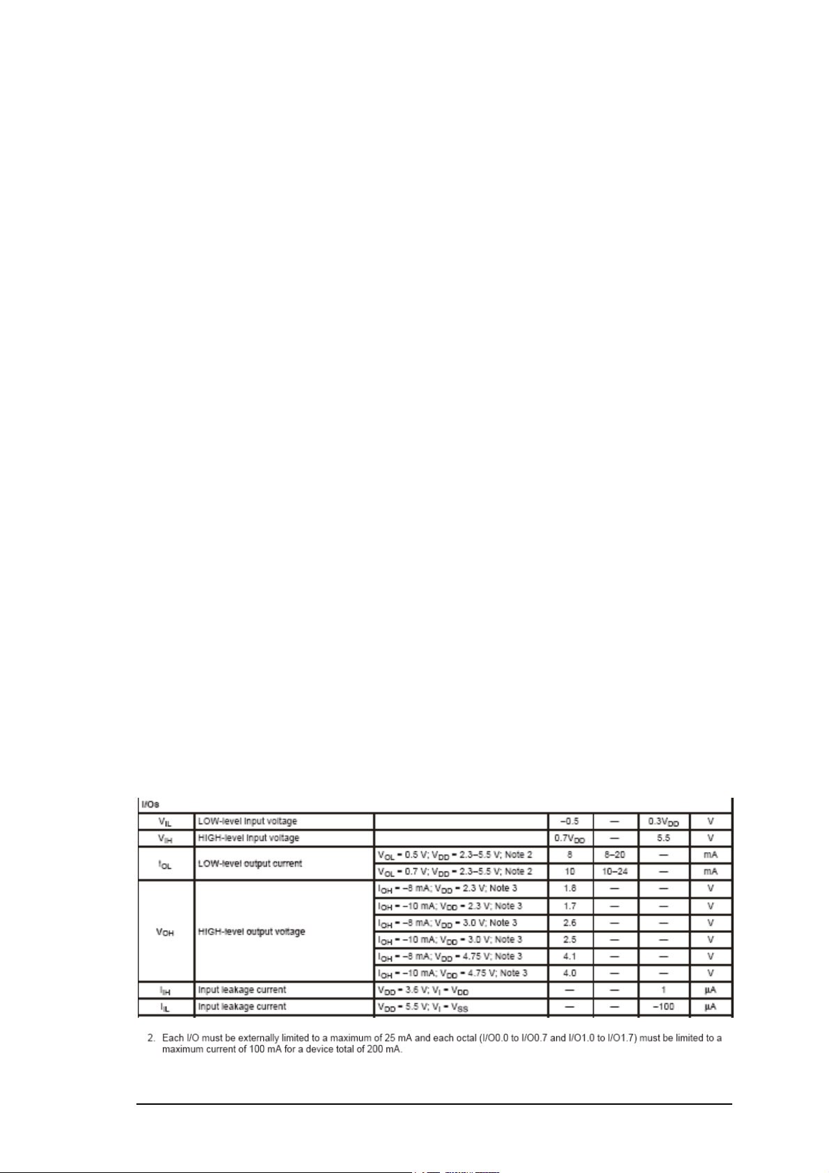
4.8.3 Electrical Characteristics
Electrical Characteristics (3.6 V < VCC ≤≤≤≤ 5.0 V) für I/O Pins
Symbol Conditions Vcc [V] Min. Max. Unit
VIH 4.0 to 5.0 2.0 V
VIL 4.0 to 5.0 0.8 V
VOH
VOH IOH=-12mA 4.0 2.4 V
VOH IOH=-18mA 5.0 2.4 V
VOH IOH=-24mA 5.0 2.4 V
VOL
VOL IOL=12mA 5.0 0.4 V
VOL IOL=18mA 5.0 0.4 V
VOL IOL=24mA 5.0 0.5 V
Table Electrical Characteristics 1: See [2]
IOH=-100µA
IOL=100µA
5.0 Vcc-0.5 V
5.0 0.2 V
Desktop Transceiver SFX-TAP4_2/C, V0.1, Technical Description 13
Page 14

Electrical Characteristics (2.7 V < V
≤≤≤≤ 3.6 V) for I/O Pins
CC
Symbol Conditions Vcc [V] Min. Max. Unit
VIH 2.7 to 3.6 2.0 V
VIL 2.7 to 3.6 0.8 V
VOH
IOH=-100µA
2.7 to 3.6 Vcc-0.2 V
VOH IOH=-12mA 2.7 2.4 V
VOH IOH=-18mA 3.0 2.4 V
VOH IOH=-24mA 3.0 2.4 V
VOL
IOL=100µA
2.7 to 3.6 0.2 V
VOL IOL=12mA 2.7 0.4 V
VOL IOL=18mA 3.0 0.4 V
VOL IOL=24mA 3.0 0.55 V
Table Electrical Characteristics 2: See [2]
Electrical Characteristics (2.3 V ≤≤≤≤ VCC ≤≤≤≤ 2.7 V) for I/O Pins
Symbol Conditions Vcc [V] Min. Max. Unit
VIH 2.3 to 2.7 1.6 V
VIL 2.3 to 2.7 0.7 V
VOH
IOH=-100µA
2.3 to 2.7 Vcc-0.2 V
VOH IOH=-6mA 2.3 2.0 V
VOH IOH=-12mA 2.3 1.8 V
VOH IOH=-18mA 2.3 1.7 V
VOL
IOL=100µA
2.3 to 2.7 0.2 V
VOL IOL=12mA 2.3 0.4 V
VOL IOL=18mA 2.3 0.6 V
Table Electrical Characteristics 3: See [2]
Electrical Characteristics (1.8 V ≤≤≤≤ VCC < 2.3 V) for I/O Pins
Symbol Conditions Vcc [V] Min. Max. Unit
VIH 1.8 to 2.3 0.65xVCC V
VIL 1.8 to 2.3 0.35xVCC V
VOH
IOH=-100µA
1.8 to 2.3 Vcc-0.2 V
VOH IOH=-6mA 1.8 1.3 V
VOL
IOL=100µA
1.8 to 2.3 0.2 V
VOL IOL=6mA 1.8 0.3 V
Table Electrical Characteristics 4: See [2]
V
V
HIGH Level Input Voltage V
IH
HIGH Level Output Voltage V
OH
LOW Level Input Voltage
OL
LOW Level Output Voltage
OL
14 Desktop Transceiver SFX-TAP4_2/C, V0.1, Technical Description
Page 15

4.9 Input Stage
The input stage consists of a High-Speed comparator. Following operating conditions are
recommended:
VCC 5.0 V
Programmable Threshold 0.0 to 3.0 V
Max. Input Voltage Range -0.3 V to 5.5 V
5 Software Settings of the Testbus Interface
5.1 TCK Frequency
The effective test speed is defined by software access time and frequency of TCK. The TCK
frequency can be freely programmed in the range of 500 Hz ... 20/50/80 MHz. Thee maximum
TCK frequency is given by the SCANFLEX controller type.
Controller Type Max. TCK
[MHz]
A
B
C
Die TCK frequency is generated following this formula: x*(12MHz+n*0.25MHz)/2
Frequency
Range
1
2
3
4
The values of m, n, and x are regarding the set TCK frequency calculated by software SYSTEM
CASCON/ POLARIS and limited by the controller type.
The TCK frequency is set as follow:
Move the mouse cursor to OPTIONS / UUT. Select the index card Testbus. Type-in the wanted
frequency. Red colour indicates a wrong parameter.
Min.
[MHz]
50 80 0.5 2% 0 112
12.0 50.0 0.25 2% 0 0...152
6 12.0 0.125 2% 1 0...47
0.0005 6 0.25/2m 2% 2..15 0..47
20
50
80
Max.
[MHz]
Resolution
[MHz]
Tolerance Value
for m
Value
for m
m
Value
for x
2
1
1
1
Desktop Transceiver SFX-TAP4_2/C, V0.1, Technical Description 15
Page 16

Valid parameters (black) are accepted here even in cases outside the controller
specific range as they are depending on the setting of the UUT.
All settings in this index card don’t have any impact to SCANFLEX products.
Voltages and delay values are defined in a further entry field.
Figure 7: TCK Setting
16 Desktop Transceiver SFX-TAP4_2/C, V0.1, Technical Description
Page 17

5.2 TAP Specific Settings
The system SCANFLEX supports up to 8 independent TAPs. The SFX-TAP2(4)/C supports two
or four TAPs respectively. Each TAP can be configured in its properties individually. These are
the TAP specific settings:
• Aktivierung der TAPs
• Testbus output and Input voltages
• Inline resistor for outputs
• Pull down resistor for inputs
• activation of the power relay
• ADYCS II ™ - the UUT-TCK-TDO delay
The TAP specific settings are made as follow:
First go to View / Tester Configuration. Alternatively, you may use the icon. The purpose
is to create a configuration for a given hardware constellation. In cases, no Tester
Configuration is existing yet, it must be created. For this, press Configuration in the left panel.
Press the button ‚new’ in the right panel. Type in the name of the new configuration. In this case
use SFX_TAP4. Confirm with OK.
Desktop Transceiver SFX-TAP4_2/C, V0.1, Technical Description 17
Page 18

Figure 8: Define a new Configuration
Now select the just defined configuration.
On the right side, select SFX Contoller in the group Modul types. Press button Insert.
Figure 9: Insert Controller
Select SFX_controller in the left panel.
Press the button Auto detect on the right.
18 Desktop Transceiver SFX-TAP4_2/C, V0.1, Technical Description
Page 19

Figure 10: Auto Detection
The result of successful detection is shown in the right panel. The recognized SCANFLEX
hardware is inserted under SFX-HS (SFX-LS1 and SFX-LS2).
In our example, a SFX-TAp4 has been recognized which appears as SFX_TAP_splitter_4_1 in
the left panel. Again, select the recognized hardware and after pressing the Enable button it is
activated for the current UUT.
Figure 11: Enable der Configuration
Desktop Transceiver SFX-TAP4_2/C, V0.1, Technical Description 19
Page 20

As a result of successful enable, you can see in the right panel a further register named Project
Parameters. There, all current parameters are displayed. They can be modified there by Edit.
Figure 12: Overview of project parameters
The TAP settings can be changed by selecting the register TAP. The next figure shows the TAP
specific parameters.
Figure 13: Entry Mask for TAP Parameter
20 Desktop Transceiver SFX-TAP4_2/C, V0.1, Technical Description
Page 21

Since in the example one SFX-TAP4 is connected with the SCANFLEX controller, four sub
registers appear in the register TAP, one per TAP. This allows TAP related definition of the
values.
Moving the mouse cursor to an entry area and waiting 1 sec, the allowed value
range is displayed. Wrong Parameters are displayed in red and automatic
limitation to minimum / maximum are set for those.
Parameters shown in figure 13 are default. They are chosen for each new
configuration. All parameters max be changed by the user.
For more information about configuration refer to SYSTEM CASCON documentation [1].
5.2.1 TIC Type
Using the scrollbar Type (see figure 13), you can select the TIC type. Type 01 must be selected
for operation.
For de-activation, select None. It removes a TAP from the configuration without deleting it from
the SFX-TAPx. For this purpose, it is switched off and no other values can be defined.
5.2.2 Output Voltage
The output voltage can be defined within following limits:
Parameter Min.
[V]
Output Voltage
The voltage entry is set in DH (see figure 13). The applicable output driver is given by the
defined voltage. More information can be found in chapter 4.8.
1.8 4.5 0.05 3.3 0.1
Max.
[V]
Resolution
[V]
Default
[V]
Accuracy
[V]
5.2.3 Input Voltage
The Input voltage is applicable within following limits:
Parameter Min.
[V]
Input voltage
The voltage entry is set in EH (see figure 13). It is a HIGH threshold. Voltages above will be
understood as logic High, otherwise Low.
0.0 3.0 0.05 1.0 0.1
Max.
[V]
Resolution
[V]
Default
[V]
Accuracy
[V]
Desktop Transceiver SFX-TAP4_2/C, V0.1, Technical Description 21
Page 22

5.2.4 Inline Resistor
The Inline resistors are applied to all TAP outputs (TCK, TMS, TDO and /TRST) with the same
value. Following values can be selected (see figure 13):
• Tristate --> the driver stays in tristate mode during test execution
• 33Ω
• 22Ω (default)
• 15Ω
These resistors form with possibly existing resistors on the UUT voltage divider
and can affect the operation. Those cases can be compensated by increasing the
output voltage.
5.2.5 Pull Down Resistor
The Pull Down resistor affects the TDI input only. The following values can be set:
• Open --> no Pull down
• 1kΩ (default)
• 330Ω
• 220Ω
5.2.6 Power Relays
The Power Relays is activated by the Checkbox Power relay (see figure 14). With activation, all
power relays are controlled to the on-state with execution start. The following delay parameter
ensures stable relay contact position and power-up of the UUT before the test itself starts. Since
the delay time can be defined per TAP individually, the largest time determines the starting time
of the test when using more than one TAP. After finishing the test, the relays return to the off
state. For further information about Power Relays refer to chapter 4.6.
5.2.7 ADYCS II™
ADYCS™ (Active Delay Compensation) allows data transmission along the TAP cable
independent from the distance to UUT. The UUT and cable design determine the maximum
TCK frequency. The Feature ADYCS™ II is supported by all types of SCANFLEX controllers.
For correct setting, notify the time delay of the UUT. Enter the value in Delay below EH, see
figure 13. Delay corresponds to t
(∆t) is entered in the text field TCK TDO delay delta. That value is global for all TAPs.
For better understanding see the timing diagram in figure 14.
in figure 14. The inaccuracy / tolerance of the time delay
delay
22 Desktop Transceiver SFX-TAP4_2/C, V0.1, Technical Description
Page 23

T
TCK
TCK
t
delay
TDO
TDO mit ∆t
+ ∆t + ∆t- ∆t - ∆t
f
= 1 / T
TCK
Figure 14: Timing diagram for UUT TCK-TDO delay
TCK
t
delay
The delay time Delay (t
) to be entered is the elapsing time between falling TCK edge on the
delay
TAP/PIP connector of the SFX-TAP4 (SFX-TAP2) until arriving the UUT’s TDO response on the
same connector.
Note, Delay (t
) covers both, time delay of the UUT and cable.
delay
TCK TDO delay delta (∆t) is the tolerance of the time delay. The higher the wanted TCK
frequency is, the more precise ∆t has to be. The software calculates the TCK frequency
following this formula:
F
<= 1 / (4 x (∆∆∆∆t + 2 ns))
TCK
Maximum values of TCK TDO delay delta (∆t), in order to get a particular TCK frequency:
• TCK 20 MHz --> max TCK TDO delay delta = 10 ns
• TCK 30 MHz --> max TCK TDO delay delta = 6 ns
• TCK 50 MHz --> max TCK TDO delay delta = 3 ns
• TCK 80 MHz --> max TCK TDO delay delta = 1 ns
Figure 14 shows a window defined by +∆t and - ∆t. Within this window the TDO is expected.
Due to the nature of Boundary Scan a rising edge must appear only after that window. The
timing difference must be in the minimum as the window itself in order to get an independence
from the time delay.
The conclusion is: The SW has to reduce the TCK frequency depending on ∆t.
Desktop Transceiver SFX-TAP4_2/C, V0.1, Technical Description 23
Page 24

Example:
Target frequency: 30 MHz
Tolerance: 8 ns
Software setting: 25 MHz (1 / (4 x (8 ns + 2 ns)) = 25 MHz)
The typical time delay value fort he cable is about 5 ns / m. Multiply this by to
because of the to and from signal propagation.
Example 1:
Hardware configuration: Scan Trainer II (GOEPEL) as UUT plus 50 cm flat cable to controller:
Cable delay + UUT delay = 2 x 2.5 ns + 10 ns = 15 ns
The UUT delay was theoretically calculated and proved by measuring: 10 ns.
Note: Measure the UUT delay:
- set the TCK frequency <= 1 MHz in SYSTEM CASCON
- scope channel 1 to TDO of the UUT
- scope channel 2 to TCK of the UUT
- trigger the scope with channel 1 (no matter which edge)
The t
is the time between falling edege of the TCK and a change of TDO
delay
TCK
t
delay
TDO
Figure 15: Measure the UUT TCK-TDO delay
24 Desktop Transceiver SFX-TAP4_2/C, V0.1, Technical Description
Page 25

5.2.8 Testbus Signals on TAP/PIP User Interface
All Testbus signals are provided on the connector TAP/PIP (SCSI68) (see TAP/PIP User
interface).
5.2.9 SCP Controller
The Desktop Transceiver SFX-TAP2/C allows the control of „SCP Modules“. These modules
typically provide additional BScan test resources in order to increase the test coverage of a
board. Typical application is testing through edge connectors.
Desktop Transceiver SFX-TAP4_2/C, V0.1, Technical Description 25
Page 26

6 Appendix
6.1 TAP/PIP : User Interface SFX-TAP4/C
GND
PIP 4.6
PIP 4.4
PIP 4.2
PIP 4.0
PIP 3.6
PIP 3.4
PIP 3.2
PIP 3.0
GND
PIP 2.6
PIP 2.4
PIP 2.2
PIP 2.0
PIP 1.6
PIP 1.4
PIP 1.2
PIP 1.0
D-AUX3
TRG0
TRG1
RSV
TDI3
TCK3
GND
TDI4
TDI2
TCK2
GND
TCK4
TDI1
TCK1
/TRST
34
33
32
31
30
29
28
27
26
25
24
23
22
21
20
19
18
17
16
15
14
13
12
11
10
68
67
66
65
64
63
62
61
60
59
58
57
56
55
54
53
52
51
50
49
48
47
46
45
44
9
8
7
6
5
3
2
1+ 3.3V
43
42
41
40
39
38
37
36
35
+ 5.0V
PIP 4.7
PIP 4.5
PIP 4.3
PIP 4.1
PIP 3.7
PIP 3.5
PIP 3.3
PIP 3.1
GND
PIP 2.7
PIP 2.5
PIP 2.3
PIP 2.1
PIP 1.7
PIP 1.5
PIP 1.3
PIP 1.1
GND
GND
GND
GND
GND
TDO3
TMS3
D-AUX2
D-AUX1
TDO2
TMS2
TDO4
TMS44
TDO1
TMS1
GND
Figure 16: Pin assignment User Interface TAP/PIP connector for SFX-TAP4/C
26 Desktop Transceiver SFX-TAP4_2/C, V0.1, Technical Description
Page 27

6.2 TAP/PIP : User Interface SFX-TAP2/C
GND
PIP 4.6
PIP 4.4
PIP 4.2
PIP 4.0
PIP 3.6
PIP 3.4
PIP 3.2
PIP 3.0
GND
PIP 2.6
PIP 2.4
PIP 2.2
PIP 2.0
PIP 1.6
PIP 1.4
PIP 1.2
PIP 1.0
D-AUX3
TRG0
TRG1
RSV
SCP-TDI
SCP-TCK
GND
RSV
TDI2
TCK2
GND
RSV
TDI1
TCK1
/TRST
34
33
32
31
30
29
28
27
26
25
24
23
22
21
20
19
18
17
16
15
14
13
12
11
10
68
67
66
65
64
63
62
61
60
59
58
57
56
55
54
53
52
51
50
49
48
47
46
45
44
9
8
7
6
5
3
2
1+ 3.3V
43
42
41
40
39
38
37
36
35
+ 5.0V
PIP 4.7
PIP 4.5
PIP 4.3
PIP 4.1
PIP 3.7
PIP 3.5
PIP 3.3
PIP 3.1
GND
PIP 2.7
PIP 2.5
PIP 2.3
PIP 2.1
PIP 1.7
PIP 1.5
PIP 1.3
PIP 1.1
GND
GND
GND
GND
GND
SCP-TDO
SCP-TMS
D-AUX2
D-AUX1
TDO2
TMS2
RSV
RSV4
TDO1
TMS1
GND
Figure 17: Pin assignment User Interface TAP/PIP connector for SFX-TAP2/C
Desktop Transceiver SFX-TAP4_2/C, V0.1, Technical Description 27
Page 28

7 Order Information
Desktop Transceiver SFX-TAP4/C STT-010
Desktop Transceiver SFX-TAP2/C STT-011
8 References
[1] - User Manual „SYSTEM CASCON“, GÖPEL electronic GmbH - 2005
[2] - CION: Configurable I/O Network, V1.4, Data Sheet GOEPEL electronic GmbH 2002
[3]..- PCA9555 Product data sheet, Supersedes the data of 2004 Jul 27, Philips
Semiconductors, 2004 Sep 30
28 Desktop Transceiver SFX-TAP4_2/C, V0.1, Technical Description
 Loading...