

MEMORY MODULE
GOODRAM zastrzega prawo do zmian w specyfikacji i opisach produktu w każdej chwili bez uprzedniej informacji.
Product Sheet | IRDM X | V1.0 | © Wilk Elektronik S.A. - GOODRAM
IR-XR 3000 D4 64 L16 S 8G
IRDM X RED
DDRIV MODULE
PART NUMBERING
SYSTEM
SPEED / DATA TRANSFER 3000Mhz / PC4-24000
MODULE TYPE DDR4 SDRAM DIMM
MODULE DATA WIDTH 64
CAS LATENCY 16
SINGLE RANK
MODULE DENSITY 8GB
PART NUMBER
IR-XR3000D464L16S/8G
MODULE TYPE
DDR4 SDRAM DIMM
MODULE DENSITY
8GB
MODULE DATA WIDTH
64
DRAM COMPONENT ORAGNIZATION
1024Mx8
NUMBER OF DRAM COMPONENTS
8 NUMBER OF MODULE RANKS
1 NUMBER OF MODULE SIDES
1
REGISTERED
NO
ECC SUPPORT
NO PIN COUNT
288 PIN
SUPPLY VOLTAGE
1,2V-1,35V
INTERFACE
PSEUDO OPEN DRAIN 1.2V (POD12)
CAS LATENCY
16 RAS# TO CAS# DELAY, tRCD
18 ROW PRECHARGE TIME, tRP
18 ACTIVE TO PRECHARGE TIME, tRAS
36
PCB TYPE
DDR4 SDRAM DIMM
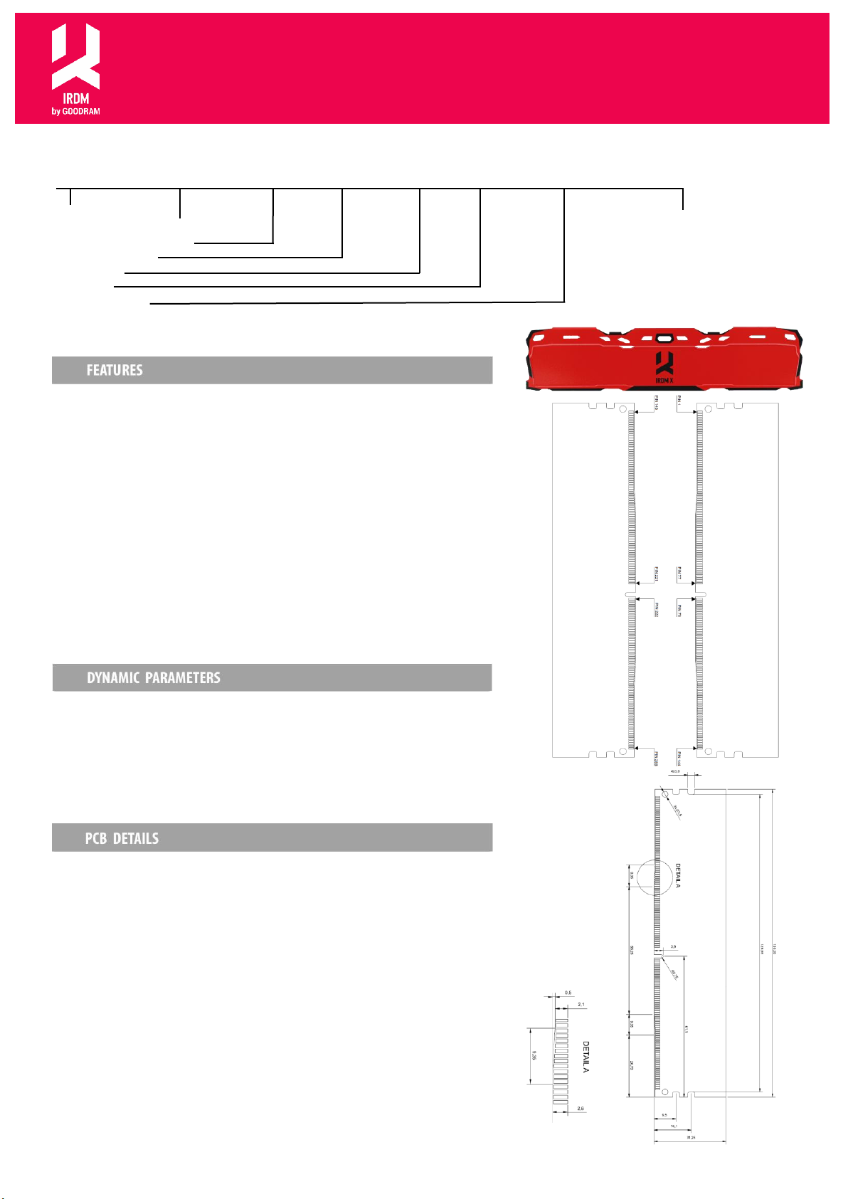
BOARD DIMENSIONS
133,35 x 31,25mm ± 0,1mm
BOARD THICKNESS
1,4mm ± 0,1mm
DRAM PACKAGE INFORMATION
FBGA, x8bit
CONTACT PADS (PIN)
GOLD PLATED

MEMORY MODULE
GOODRAM zastrzega prawo do zmian w specyfikacji i opisach produktu w każdej chwili bez uprzedniej informacji.
Product Sheet | IRDM X | V1.0 | © Wilk Elektronik S.A. - GOODRAM
Byte
Description
HEX
DEC
0
Number of Serial PD Bytes Written / SPD Device Size / CRC Coverage 1 2
0x23
35
1
SPD Revision
0x11
17
2
Key Byte / DRAM Device Type
0x0c
12 3 Key Byte / Module Type
0x02
2 4 SDRAM Density and Banks
0x85
133
5
SDRAM Addressing
0x21
33
6
SDRAM Package Type
0x00
0
7
SDRAM Optional Features
0x08
8 8 SDRAM Thermal and Refresh Options
0x00
0 9 Other SDRAM Optional Features
0x40
64
10
Reserved -- must be coded as 0x00
0x00
0
11
Module Nominal Voltage, VDD
0x03
3
12
Module Organization
0x01
1
13
Module Memory Bus Width
0x03
3
14
Module Thermal Sensor
0x00
0
15
Extended module type
0x00
0
16
Reserved -- must be coded as 0x00
0x00
0
17
Timebases
0x00
0
18
SDRAM Minimum Cycle Time (tCKAVGmin)
0x06
6
19
SDRAM Maximum Cycle Time (tCKAVGmax)
0x0d
13
20
CAS Latencies Supported, First Byte
0xf8
248
21
CAS Latencies Supported, Second Byte
0x3f
63
22
CAS Latencies Supported, Third Byte
0x00
0
23
CAS Latencies Supported, Fourth Byte
0x00
0
24
Minimum CAS Latency Time (tAAmin)
0x6e
110
25
Minimum RAS to CAS Delay Time (tRCDmin)
0x6e
110
26
Minimum Row Precharge Delay Time (tRPmin)
0x6e
110
27
Upper Nibbles for tRASmin and tRCmin
0x11
17
28
Minimum Active to Precharge Delay Time (tRASmin), Least Significant Byte
0x00
0
29
Minimum Active to Active/Refresh Delay Time (tRCmin), Least Significant Byte
0x6e
110
30
Minimum Refresh Recovery Delay Time (tRFC1min), LSB
0xf0
240
31
Minimum Refresh Recovery Delay Time (tRFC1min), MSB
0x0a
10
32
Minimum Refresh Recovery Delay Time (tRFC2min), LSB
0x20
32
33
Minimum Refresh Recovery Delay Time (tRFC2min), MSB
0x08
8
34
Minimum Refresh Recovery Delay Time (tRFC4min), LSB
0x00
0
35
Minimum Refresh Recovery Delay Time (tRFC4min), MSB
0x05
5
36
Minimum Four Activate Window Time (tFAWmin), Most Significant Nibble
0x00
0
37
Minimum Four Activate Window Time (tFAWmin), Least Significant Byte
0xa8
168
38
Minimum Activate to Activate Delay Time (tRRD_Smin), different bank group
0x18
24
39
Minimum Activate to Activate Delay Time (tRRD_Lmin), same bank group
0x28
40
40
Minimum CAS to CAS Delay Time (tCCD_Lmin), same bank group
0x28
40
41-59
Reserved -- must be coded as 0x00
0x00
0

MEMORY MODULE
GOODRAM zastrzega prawo do zmian w specyfikacji i opisach produktu w każdej chwili bez uprzedniej informacji.
Product Sheet | IRDM X | V1.0 | © Wilk Elektronik S.A. - GOODRAM
60
Connector to SDRAM Bit Mapping
0x16
22
61
Connector to SDRAM Bit Mapping
0x36
54
62
Connector to SDRAM Bit Mapping
0x16
22
63
Connector to SDRAM Bit Mapping
0x36
54
64
Connector to SDRAM Bit Mapping
0x16
22
65
Connector to SDRAM Bit Mapping
0x36
54
66
Connector to SDRAM Bit Mapping
0x16
22
67
Connector to SDRAM Bit Mapping
0x36
54
68
Connector to SDRAM Bit Mapping
0x00
0
69
Connector to SDRAM Bit Mapping
0x00
0
70
Connector to SDRAM Bit Mapping
0x16
22
71
Connector to SDRAM Bit Mapping
0x36
54
72
Connector to SDRAM Bit Mapping
0x16
22
73
Connector to SDRAM Bit Mapping
0x36
54
74
Connector to SDRAM Bit Mapping
0x16
22
75
Connector to SDRAM Bit Mapping
0x36
54
76
Connector to SDRAM Bit Mapping
0x16
22
77
Connector to SDRAM Bit Mapping
0x36
54
78-116
Reserved -- must be coded as 0x00
0x00
0
117
Fine Offset for Minimum CAS to CAS Delay Time (tCCD_Lmin), same bank group
0x00
0
118
Fine Offset for Minimum Activate to Activate Delay Time (tRRD_Lmin), same bank group
0x9c
156
119
Fine Offset for Minimum Activate to Activate Delay Time (tRRD_Smin), different bank group
0x00
0
120
Fine Offset for Minimum Activate to Activate/Refresh Delay Time (tRCmin)
0x00
0
121
Fine Offset for Minimum Row Precharge Delay Time (tRPmin)
0x00
0
122
Fine Offset for Minimum RAS to CAS Delay Time (tRCDmin)
0x00
0
123
Fine Offset for Minimum CAS Latency Time (tAAmin)
0x00
0
124
Fine Offset for SDRAM Maximum Cycle Time (tCKAVGmax)
0xe7
231
125
Fine Offset for SDRAM Minimum Cycle Time (tCKAVGmin)
0x00
0
126
CRC for Base Configuration Section, Least Significant Byte
0x74
116
127
CRC for Base Configuration Section, Most Significant Byte
0x73
115
128-511
Module Specific SPD Bytes
 Loading...