

Goodram IR-W2400D464L15S-16GDC Technical data
MEMORY MODULE
IR-W 2400 D4 64 L15 S 16GDC
GOODRAM IRDM WHITE
DDRIV MODULE PART
NUMBERING SYSTEM
SPEED / DATA TRANSFER 2400MHz / PC4-19200
MODULE TYPE DDR4 SDRAM DIMM
MODULE DATA WIDTH 64
CAS LATENCY 15
SINGLE RANK
MODULE DENSITY 16GB DUAL CHANNEL
PART NUMBER
IR-W2400D464L15S/16GDC
MODULE TYPE
DDR4 SDRAM DIMM
MODULE DENSITY
2x8GB
MODULE DATA WIDTH
64
DRAM COMPONENT ORAGNIZATION
1024Mx8
NUMBER OF DRAM COMPONENTS
8 NUMBER OF MODULE RANKS
1 NUMBER OF MODULE SIDES
1
REGISTERED
NO
ECC SUPPORT
NO
PIN COUNT
288 PIN
SUPPLY VOLTAGE
1,2V INTERFACE
PSEUDO OPEN DRAIN 1.2V (POD12)
CAS LATENCY
15 RAS# TO CAS# DELAY, tRCD
15 ROW PRECHARGE TIME, tRP
15 ACTIVE TO PRECHARGE TIME, tRAS
38
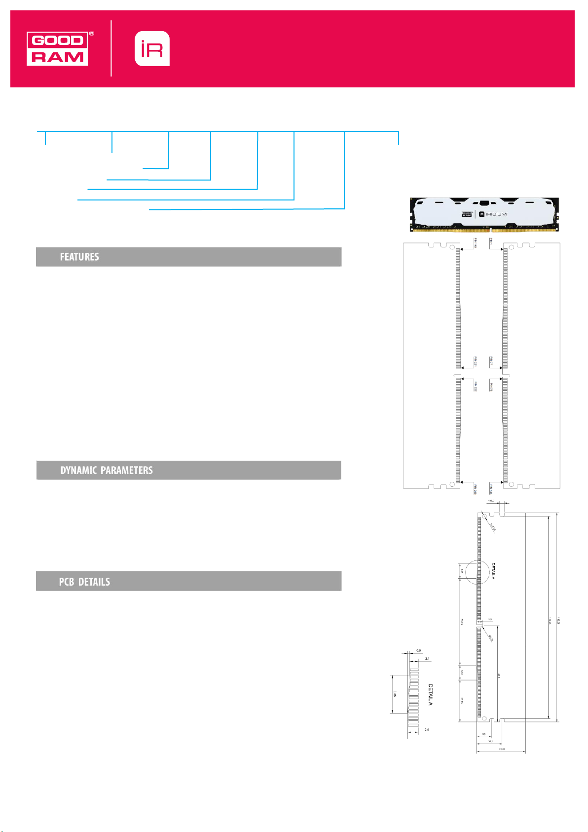
PCB TYPE
DDR4 SDRAM DIMM
BOARD DIMENSIONS
133,35 x 31,25mm ± 0,1mm
BOARD THICKNESS
1,4mm ± 0,1mm
DRAM PACKAGE INFORMATION
FBGA, x8bit
CONTACT PADS (PIN)
GOLD PLATED
GOODRAM may make changes to specifications and product descriptions at any time, without notice.
Product Sheet | IRDM | V0.1 | © Wilk Elektronik SA – GOODRAM

MEMORY MODULE
Byte
Description
HEX
DEC
0
Number of Serial PD Bytes Written / SPD Device Size / CRC Coverage 1 2
0x23
35
1
SPD Revision
0x11
17
2
Key Byte / DRAM Device Type
0x0c
12 3 Key Byte / Module Type
0x02 2 4
SDRAM Density and Banks
0x85
133
5
SDRAM Addressing
0x21
33
6
SDRAM Package Type
0x00 0 7
SDRAM Optional Features
0x08 8 8
SDRAM Thermal and Refresh Options
0x00 0 9
Other SDRAM Optional Features
0x60
96
10
Reserved -- must be coded as 0x00
0x00 0 11
Module Nominal Voltage, VDD
0x03 3 12
Module Organization
0x01 1 13
Module Memory Bus Width
0x03 3 14
Module Thermal Sensor
0x00 0 15
Extended module type
0x00 0 16
Reserved -- must be coded as 0x00
0x00 0 17
Timebases
0x00 0 18
SDRAM Minimum Cycle Time (tCKAVGmin)
0x07 7 19
SDRAM Maximum Cycle Time (tCKAVGmax)
0x0c
12
20
CAS Latencies Supported, First Byte
0xfc
252
21
CAS Latencies Supported, Second Byte
0x03 3 22
CAS Latencies Supported, Third Byte
0x00 0 23
CAS Latencies Supported, Fourth Byte
0x00 0 24
Minimum CAS Latency Time (tAAmin)
0x64
100
25
Minimum RAS to CAS Delay Time (tRCDmin)
0x64
100
26
Minimum Row Precharge Delay Time (tRPmin)
0x64
100
27
Upper Nibbles for tRASmin and tRCmin
0x11
17
28
Minimum Active to Precharge Delay Time (tRASmin), Least Significant Byte
0x00 0 29
Minimum Active to Active/Refresh Delay Time (tRCmin), Least Significant Byte
0x64
100
30
Minimum Refresh Recovery Delay Time (tRFC1min), LSB
0xf0
240
31
Minimum Refresh Recovery Delay Time (tRFC1min), MSB
0x0a
10
32
Minimum Refresh Recovery Delay Time (tRFC2min), LSB
0x20
32
33
Minimum Refresh Recovery Delay Time (tRFC2min), MSB
0x08 8 34
Minimum Refresh Recovery Delay Time (tRFC4min), LSB
0x00 0 35
Minimum Refresh Recovery Delay Time (tRFC4min), MSB
0x05 5 36
Minimum Four Activate Window Time (tFAWmin), Most Significant Nibble
0x00 0 37
Minimum Four Activate Window Time (tFAWmin), Least Significant Byte
0xa8
168
38
Minimum Activate to Activate Delay Time (tRRD_Smin), different bank group
0x1e
30
39
Minimum Activate to Activate Delay Time (tRRD_Lmin), same bank group
0x2b
43
40
Minimum CAS to CAS Delay Time (tCCD_Lmin), same bank group
0x2b
43
41-59
Reserved -- must be coded as 0x00
0x00
0
GOODRAM may make changes to specifications and product descriptions at any time, without notice.
Product Sheet | IRDM | V0.1 | © Wilk Elektronik SA – GOODRAM
 Loading...