

GOOD-ARK 1N759, 1N758, 1N757, 1N756, 1N755 Datasheet
...
Features
Silicon Planar Zener Diodes
Standard Zener voltage tolerance is 10%. Add suffix A
for
5% tolerance. Other tolerances, non standard and
higher Zener voltages upon request.
1N746 THRU 1N759
SILICON PLANAR ZENER DIODES
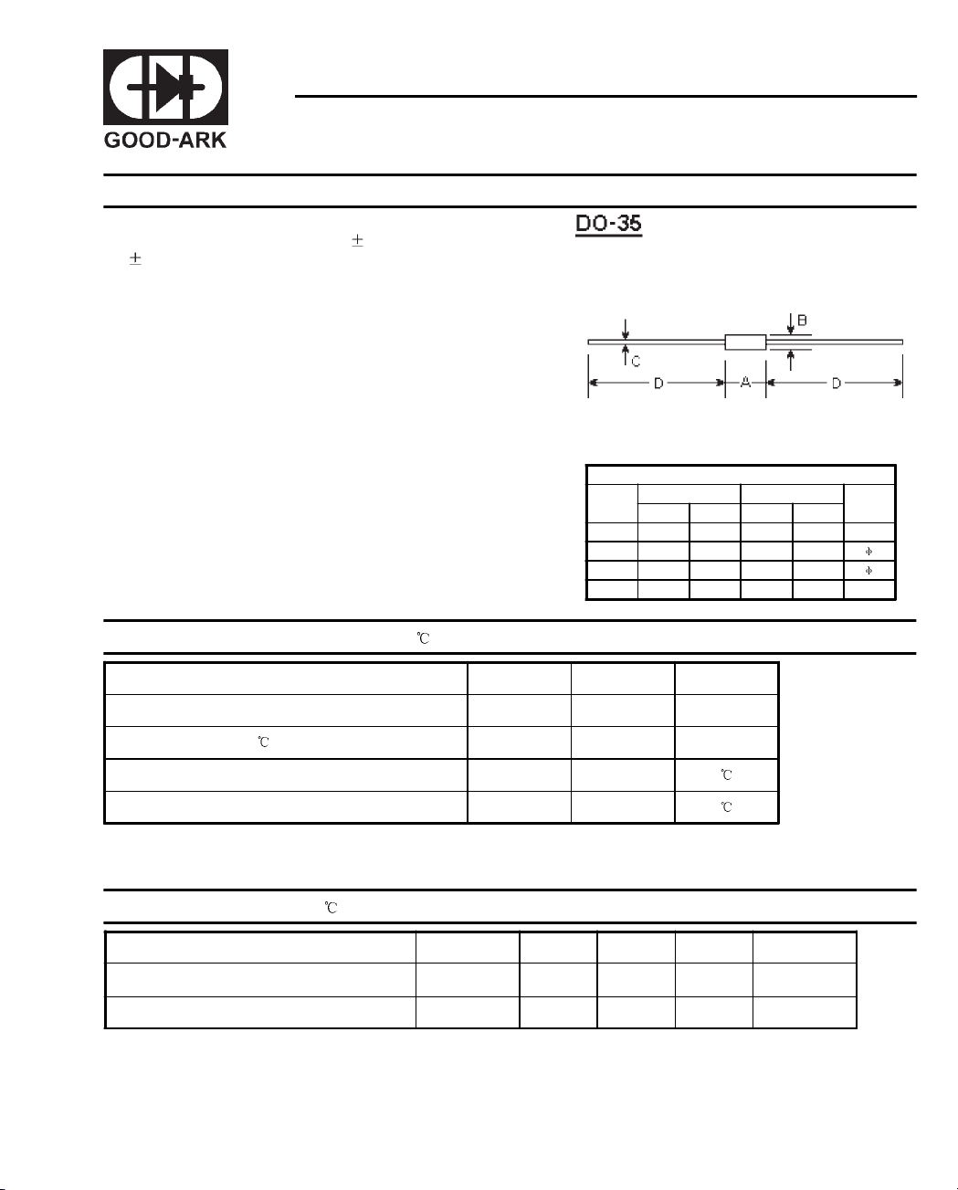
DIMENSIONS
DIM
A - 0.154 - 3.9
B - 0.075 - 1.9
C - 0.020 - 0.52
D 1.083 - 27.50 -
inches mm
Min. Max. Min. Max.
Note
Absolute Maximum Ratings (T
Zener current see Table "Characteristics"
Power dissipation at T
Junction Temperature T
Storage temperature range T
Note:
(1) Valid provided that leads at a distance of 8 mm from case are kept at ambient temperature.
Characteristics
Thermal resistance
junction to ambient Air
Forward voltage at I
Note:
(1) Valid provided that leads at a distance of 8 mm from case are kept at ambient temperature.
=50 P
amb
T
=25
at
amb
=200mA V
F
=25 )
a
Symbols Values Units
tot
j
S
Symbols Min. Typ. Max. Units
R
thA
F
1
1)
400
175
-65 to +175
- - 0.3
--1.2 V
mW
1)
K/mW

1)
Type
Zener voltage range
V
I
znom
Maximum
Zener
Impedence
at I
Z
ZT
ZT
ZT
Typica l
Temperature
coefficient
Maximum reverse leakage
2) at VR=1V
current I
R
T
=25 TA=150
A
Maximum
Regulator
current
I
ZM
VmA %/ uA uuA mA
1N746 3.3 20 28 -0.062 10 30 110
1N747 3.6 20 24 -0.055 10 30 100
1N748 3.9 20 23 -0.049 10 30 95
1N749 4.3 20 22 -0.036 2 30 85
1N750 4.7 20 19 -0.018 2 30 75
1N751 5.1 20 17 -0.008 1 20 70
1N752 5.6 20 11 +0.006 1 20 65
1N753 6.2 20 7 +0.022 0.1 20 60
1N754 6.8 20 5 +0.035 0.1 20 55
1N755 7.5 20 6 +0.045 0.1 20 50
1N756 8.2 20 8 +0.052 0.1 20 45
1N757 9.1 20 10 +0.056 0.1 20 40
1N758 10.0 20 17 +0.060 0.1 20 35
1N759 12.0 20 30 +0.060 0.1 20 30
Notes:
(1) Test with pulse tp=20ms.
(2) Valid provided that leads are kept at ambient temperature at a distance of 8 mm from case.
2
 Loading...