

GMT G9611DP1U, G9611DP1T, G9611CP1U, G9611CP1T, G9611BP1U Datasheet
...
Global Mixed-mode Technology Inc.
G9611
Low-Dropout, 300mA Linear Regulator with Reset
Features
300mA Output Current, with Foldback Current
Limiting
High Ripple Rejection
1.5% Output Accuracy
±±±±
2% Reset Threshold Accuracy
±±±±
Externally Programmable Reset Time Delay
Generator
Internal 300mA P-Channel Pass Transistor
320µA quiescent Current
Thermal Overload Protection
SOP 8 Package
Applications
CD ROM or DVD ROM
Slim-Type CD/DVD
DVD Player
General Description
The G9611 are low-dropout, linear regulator with
reset function supply 3.4V, 3.3V or 2.5V output for
currents up to 300mA. They are available in a
700mW SOP 8 package. Typical dropouts are
320mV at 300mA. Shutdown turns off linear regulator function. Other features include foldback current
limiting and thermal overload protection.
The reset function in G9611 detect V
hysteresis, keeping it asserted for time delay determined by external capacitor. The reset output is active low open-drain output. The detection threshold
are 3.9V or 4.2V.
The output is preset at 3.4V for the G9611A, 3.3V
for the G9611B/C, and 2.5V for G9611D. The reset
threshold is preset at 4.2V for G9611 A/B/D and
3.9V for G9611C.
level with
CC
Ordering Information
PART
NUMBER
G9611AP1x G9611A 3.4 4.2 -40°C to +85°C SOP 8L
G9611BP1x G9611B 3.3 4.2 -40°C to +85°C SOP 8L
G9611CP1x G9611C 3.3 3.9 -40°C to +85°C SOP 8L
G9611DP1x G9611D 2.5 4.2 -40°C to +85°C SOP 8L
MARKING
REGULATOR
OUTPUT VOLTAGE
Note: X Specify the packing type
U: Tape & Reel T: Tube
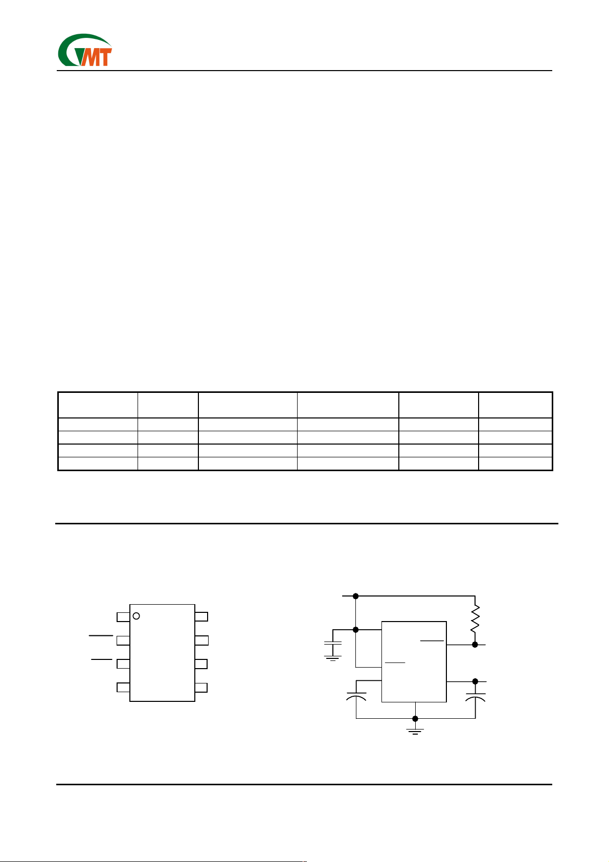
Pin configuration
RESET THRESHOLD
VOLTAGE
TEMP.
RANGE
Typical Operation Circuit
PIN-
PACKAGE
V
V
CC
CC
R
R
pull-high
pull-high
Ω
Ω
10k
10k
V
V
IN
1µF
1µF
IN
SHDN
SHDN
C
C
D
D
G9611
G9611
GND
GND
RESET
RESET
V
V
OUT
OUT
OUTPUT
OUTPUT
VOLTAGE
VOLTAGE
10µF
10µF
(Tantalum or Aluminum)
(Tantalum or Aluminum)
N.C
N.C
RESET
RESET
SHDN
SHDN
V
V
G9611
G9611
8
C
8
1
1
2
2
3
3
4
4
IN
IN
8Pin SOP
8Pin SOP
C
D
D
GND
7
GND
7
N.C
N.C
6
6
5
5
V
V
OUT
OUT
Ver: 1.2
Feb 13, 2003
TEL: 886-3-5788833
http://www.gmt.com.tw
1
Global Mixed-mode Technology Inc.
G9611
Absolute Maximum Ratings
Supply Voltage (IN or OUT to GND……..-0.3V to +6.5V
Output Short-Circuit Duration…………….…………1 min
Input Voltage …………………..…-0.3V to the greater of
(IN+0.3V) or (OUT + 0.3V)
Continuous Power Dissipation (T
Stresses beyond those listed under "Absolute Maximum Ratings" may cause permanent damage to the device. These are stress rat-
ings only, and functional operation of the device at these or any other conditions beyond those indicated in the operational sections of
the specifications is not implied. Exposure to absolute maximum rating conditions for extended periods may affect device reliability
= +25°C)…...700mW
A
Operating Temperature Range……..…. -40°C to +85°C
Junction Temperature……………….……………+160°C
Storage Temperature Range…..…..….-65°C to +160°C
Lead Temperature (soldering, 10sec)…...….…..+300°C
Electrical Characteristics
VIN=5V, CIN=1µF, C
regulators are at V
PARAMETER SYMBOL CONDITIONS MIN TYP MAX UNITS
Input Voltage VIN 2.5 6.0 V
Output Voltage (Note 1) V
Load Regulation
Line Regulation
Dropout Voltage (Note 2)
Parameter Tempco V
Ripple Rejection PSRR
Output Noise en 20Hz to 100kHz, I
Quiescent Current IQ 320 450 µA
OFF Quiescent Current I
Foldback Current Limit I
Foldback Voltage V
Thermal Shutdown Temperature TSD 160 °C
Thermal Shutdown Hysteresis
SHDN Pin Input High Threshold
SHDN Pin Input Low Threshold
Reset Threshold V
Reset Threshold Hysteresis V
Reset Threshold Tempco 40 ppm/°C
CD Delay Pin Threshold Voltage V
CD Pin Sink Current ICD VCC=1.5V, VCD=0.5V 3 4.3 mA
CD Pin Pullup Resistance RD 100 200 400 kΩ
RESET Output Current Low IOL
RESET Function Operating Voltage VOP
Note 1: (VIN-V
OUT
limits.
Note 2: Dropout Voltage is (V
example, the G9611 is tested by measuring the V
100mV below the measured value. The difference (V
Note 3: Low duty pulse techniques are used during test to maintain junction temperature as close to ambient as possible.
=10µF, SHDN =VIN, TJ =TA=25°C (Note3), unless otherwise noted. Typical values for
OUT
=5V.
IN
G9611A 3.35 3.4 3.45
G9611B/C 3.25 3.3 3.35
OUT
V
G9611D 2.45 2.5 2.55
V
I
∆
LDR
V
∆
LNR
VDO I
∆
40 ppm/°C
OUT
QOFF
LIM
FOLDBACK
TSD 30 °C
∆
V
IH_
SHDN
V
IL_
SHDN
TH-
HYS
TCD
) is limited to keep the product (I
- V
IN
) when V
OUT
=1mA to 300mA, VIN=V
OUT
(V
+0.5V) ≤ V
OUT
=300mA 320 400 mV
OUT
f=120HZ, I
f=120HZ, I
SHDN
V
OUT<VFOLDBACK
V
OUT>VFOLDBACK
0.4V
≤
OUT
OUT
6V, I
≤
IN
=30mA 70
=300mA 65
=30mA. 350
OUT
260 400 580
650 900 1200
0.6 0.78 0.95 V
1.8 2 2.3 V
0.6 0.8 1.1 V
G9611A/B/D 4.11 4.2 4.29
G9611C 3.81 3.9 3.99
G9611A/B/D 150
G9611C 130
VCC = 5V 3.5 3.9 4.3 V
V
=2.5V, V
CC
RESET
sink current>10µA
x (VIN - V
OUT
falls to 100mV below its nominal value at VIN = V
OUT
RESET
OUT
=0.4V
OUT
at VIN = V
- V
IN
+1V 6 15 mV
OUT
=25mA -8 0.3 8 mV
OUT
dB
µVRMS
140 200 µA
mA
V
mV
8 11.5 mA
0.7 0.85 V
)) from exceeding the package power dissipation
+1V. For
OUT
+1V, then VIN is lowered until V
OUT
) is then measured and defined as ∆VDO.
OUT
OUT
falls
Ver: 1.2
Feb 13, 2003
TEL: 886-3-5788833
http://www.gmt.com.tw
2
Global Mixed-mode Technology Inc.
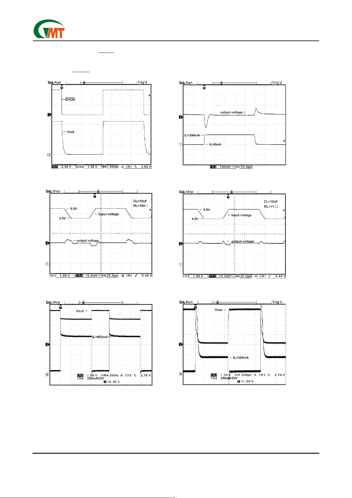
Typical Performance Characteristics
(VIN=5V,CIN=C
=10µF, SHDN =VIN, TJ=25°C, unless otherwise noted)
OUT
SHDN Pin vs. Output
Line Transient Line Transient
Load transient
G9611
Ver: 1.2
Feb 13, 2003
Over Current Response Short Circuit Response
3
TEL: 886-3-5788833
http://www.gmt.com.tw
 Loading...