

GMT G950T55U, G950T55T, G950T55D, G950T45U, G950T45T Datasheet
...
Ver: 1.6
Dec 31, 2002
TEL: 886-3-5788833
http://www.gmt.com.tw
1
G950
Global Mixed-mode Technology Inc.
2.5V 1A Regulator
Features
Output current in excess of 1A
Output voltage accuracy +3%/-1%
Quiescent current, typically 600µA
Internal short circuit current limit
Internal over temperature protection
Applications
PC motherboard
ADSL/Cable Modem
Set-Top-Box
LAN switch/Hub
Router
General Description
The G950 positive 2.5V voltage regulator features
the ability to source 1A of output current. The typical
quiescent current is 0.6mA.
Familiar regulator features such as over temperature and over current protection circuits are provided to prevent it from being damaged by abnormal operating conditions.
Ordering Information
PIN OPTION
ORDER NUMBER PACKAGE TYPE
1 2 3
G950T45U TO 252 V
IN
GND V
OUT
G950T55U TO 263 V
IN
GND V
OUT
G950T63U SOT 223 GND V
OUT
V
IN
G950T64U SOT 223 GND VIN V
OUT
G950T65U SOT 223 V
IN
GND V
OUT
G950T66U SOT 223 VIN V
OUT
GND
* For other package types and pin options, please contact us at sales @gmt.com.tw
Order Number Identification
GXXX XX X X
Packing Type
Pin Option
Package Type
Part Number
PACKAGE TYPE PIN OPTION PACKING
T3 : TO 220
1 2 3
U & D : Tape & Reel Direction
T4 : TO 252 1 : V
OUT
GND VIN T : Tube
T5 : TO 263 2 : V
OUT
VIN GND
T6 : SOT 223 3 : GND V
OUT
VIN
4 : GND V
IN
V
OUT
5 : V
IN
GND V
OUT
6 : V
IN
V
OUT
GND
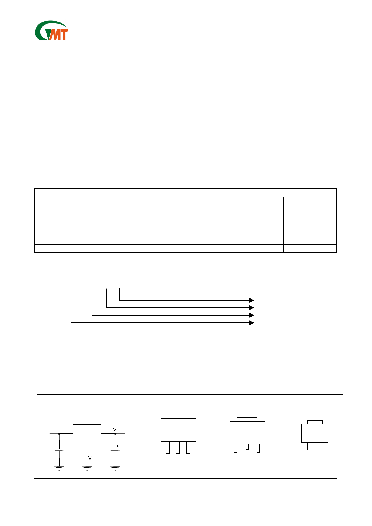
Typical Application Package Type
[Note 4] : Type of C
OUT
G950
C1
1µF
IQ
V
IN
V
OUT
I
O
C
OUT
10µF
Top View
1
3
TO 220
2
Top View
1
2
3
SOT 223
Top View
1
2
3
TO252
、、、、
263
Top View
1
3
TO 220
2
Top View
1
3
TO 220
2
Top View
1
2
3
SOT 223
Top ViewTop View
1
2
3
SOT 223
Top View
1
2
3
TO252
、、、、
263
Top View
1
2
3
TO252
、、、、
263
Ver: 1.6
Dec 31, 2002
TEL: 886-3-5788833
http://www.gmt.com.tw
2
G950
Global Mixed-mode Technology Inc.
Absolute Maximum Ratings
(Note 1)
Input Voltage……………………………………..…..…7V
Power Dissipation Internally Limited …. (Note 2)
Maximum Junction Temperature…..…………… …..150°C
Storage Temperature Range….…..-65°C ≤ T
J
≤+150°C
Lead Temperature, Time for Wave Soldering
TO 220 Package………………………………260°C, 10s
TO 252, TO 263, SOT 223 Package…….…...260°C, 4s
Continuous Power Dissipation (T
A
= + 25°C)
SOT 223
(1)
……………………….….……….………..0.8W
TO 252
(1)
………..……………….……….….………..1.0W
TO 263
(1)
………..……………….……….….………..1.6W
Note
(1)
: See Recommended Minimum Footprint.
Operating Conditions
(Note 1)
Input Voltage…………………………………….3.3V~6V
Temperature Range……………………0°C ≤ T
J
≤125°C
Electrical Characteristics
VIN =5V, IO = 1A, CIN = 1µF, C
OUT
=10 µF, All specifications apply for TA = TJ = 25°C. [Note 3]
PARAMETER CONDITIONS MIN TYP MAX UNITS
V
IN
= 5V, 10mA < IO < 1A
Output Voltage
V
IN
= 3.3V, 10mA < IO < 500mA
2.475 2.50 2.575 V
Line Regulation 3.3V < VIN < 6V, IO = 10mA 3 30 mV
V
IN
= 5V, 10mA < IO < 1A 35 50 mV
Load Regulation
V
IN
= 3.3V, 10mA < IO < 500mA 25 mV
Output Impedance 200mA DC and 100mA AC, fo = 120Hz 80
mΩ
Quiescent Current V
IN
= 5V 0.6 mA
Ripple Rejection fi = 120Hz,V
ripple
=2V
P-P,
Io = 100mA 46 dB
IO = 1A 1.15 V
IO = 500mA 420 mV
Dropout Voltage
I
O
= 100mA 200 mV
Short Circuit Current 1.6 A
Over Temperature 150
°C
Note 1:
Absolute Maximum Ratings are limits beyond which damage to the device may occur. Operating
Conditions are conditions under which the device functions but the specifications might not be guaranteed. For
guaranteed specifications and test conditions see the Electrical Characteristics.
Note 2:
The maximum power dissipation is a function of the maximum junction temperature, T
Jmax
; total thermal re-
sistance,
θ
JA
, and ambient temperature TA. The maximum allowable power dissipation at any ambient tem-
perature is T
jmax-TA
/
θ
JA
. If this dissipation is exceeded, the die temperature will rise above 150°C and IC
will go into thermal shutdown. For the G950 in SOT 223 package,
θ
JA
is 156°C/W; in TO 263 package,
θ
JA
is 75°C/W, and in the TO 252 package,
θ
JA
is 125°C/W (See recommend minimum footprint). The safe
operation in SOT 223,TO 252 & TO 263 package, it can see “Typical Performance Characteristics” (Safe
Operating Area).
Note3:
Low duty pulse techniques are used during test to maintain junction temperature as close to ambient as possible.
Note4:
The type of output capacitor should be tantalum or aluminum.
Definitions
Dropout Voltage
The input/output Voltage differential at which the
regulator output no longer maintains regulation against
further reductions in input voltage. Measured when the
output drops 100mV below its nominal value. Dropout
voltage is affected by junction temperature, load current and minimum input supply requirements.
Line Regulation
The change in output voltage for a change in input
voltage. The measurement is made under conditions
of low dissipation or by using pulse techniques such
that average chip temperature is not significantly affected.
Load Regulation
The change in output voltage for a change in load
current at constant chip temperature. The measurement is made under conditions of low dissipation or by
using pulse techniques such that average chip temperature is not significantly affected.
Maximum Power Dissipation
The maximum total device dissipation for which the
regulator will operate within specifications.
Quiescent Bias Current
Current which is used to operate the regulator chip
and is not delivered to the load.
Ver: 1.6
Dec 31, 2002
TEL: 886-3-5788833
http://www.gmt.com.tw
3
G950
Global Mixed-mode Technology Inc.
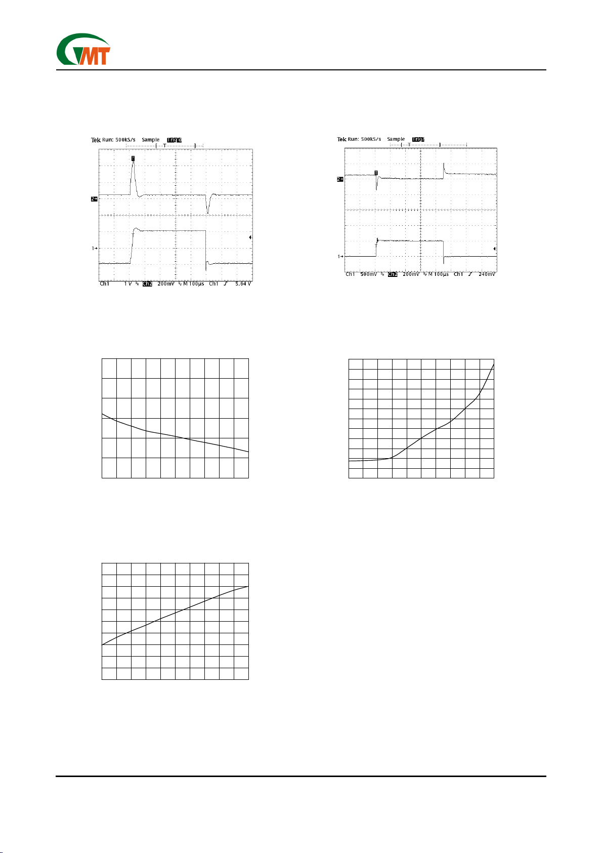
Typical Performance Characteristics
(VIN= +5V, CIN=1µF, C
OUT
=10µF, TA=25°C, unless otherwise noted.)
Ground Current vs. Load Current
0.00
0.20
0.40
0.60
0.80
1.00
1.20
1.40
1.60
1.80
2.00
0 100 200 300 400 500 600 700 800 900 1000
Load Current (mA)
Ground Current (mA)
Output Voltage vs. Load Current
2.480
2.500
2.520
2.540
2.560
2.580
2.600
0 100 200 300 400 500 600 700 800 900 1000
Load Current (mA)
Ootput Voltage (V)
Dropout Voltage vs. Load Current
0
100
200
300
400
500
600
700
800
900
1000
1100
1200
0 100 200 300 400 500 600 700 800 900 1000
Load Current (mA)
Dropout Voltage (mV)
Line Transient Load Transient
Ch1: Vin (offset=5.0V)
Ch2: Vout (offs et=2.50V)
CIN = 1uF
Iout=100mA
Ch1: Iout (1A/div)
Ch2: Vout (offs et=2.50V)
 Loading...