

GMT G936T65D, G936T65B, G936T24T, G936T24D, G936T24B Datasheet
...
Ver: 1.5
May 13, 2002
TEL: 886-3-5788833
http://www.gmt.com.tw
1
G936
Global Mixed-mode Technology Inc.
3.6V 500mA/400mA+ Low Dropout Regulator
Features
Dropout voltage typically 0.9V @ IO = 500mA
Output current in excess of 500mA/400mA+
Output voltage accuracy
±±±±
2%
Quiescent current, typically 0.6mA
Internal short circuit current limit
Internal over temperature protection
General Description
The G936 positive 3.6V voltage regulator features the
ability to source 500mA/400mA
+
of output current with
a dropout voltage of typically 0.9V/0.65V. A low quiescent current is provided. The typical quiescent current
is 0.6mA.
[+
For SOT-89 package only
]
Familiar regulator features such as over temperature
and over current protection circuits are provided to
prevent it from being damaged by abnormal operating
conditions.
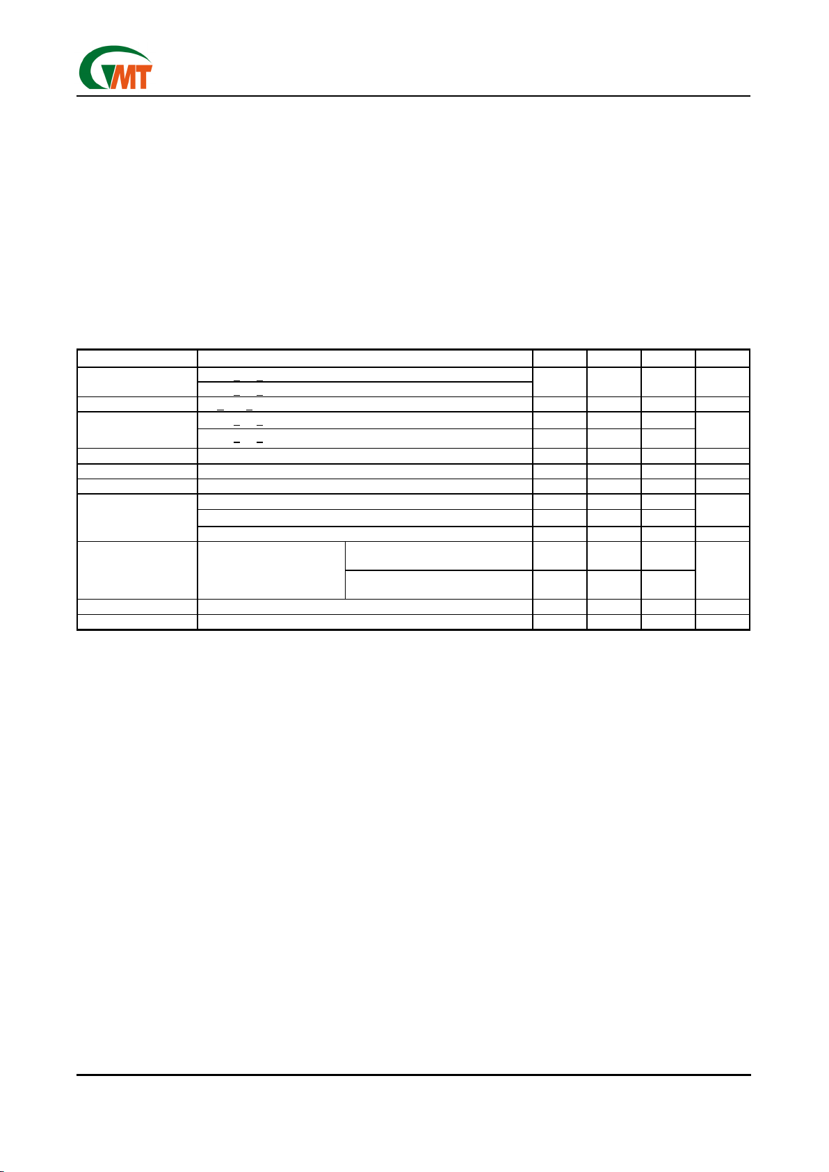
Ordering Information
PIN OPTION
ORDER NUMBER PACKAGE TYPE
1 2 3
G936T24U SOT89 GND V
IN
V
OUT
G936T65U SOT223 VIN GND V
OUT
* For other package types, pin options and package, please contact us at sales @gmt.com.tw
Order Number Identification
GXXX XX X X
Packing Type
Pin Option
Package Type
Part Number
PACKAGE TYPE PIN OPTION PACKING
T2 : SOT 89
1 2 3
U & D : Tape & Reel Direction
T6 : SOT 223 1 : V
OUT
GND VIN T : Tube
T7 : SOT 23 2 : V
OUT
VIN GND B : Bag
T8 : µTO92 3 : GND V
OUT
VIN
4 : GND V
IN
V
OUT
5 : V
IN
GND V
OUT
6 : V
IN
V
OUT
GND
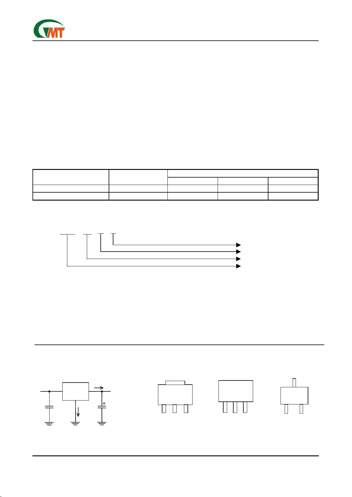
Typical Application Package Type
[Note 4] : Type of C
OUT
Top View
1
2
3
Top View
1
3
µTO 92
Top View
SOT 23
1
3
2
Top ViewTop View
1
2
3
SOT 89
、、、、
223
Top View
2
V
IN
G936
C1
1µF
IQ
V
OUT
I
O
C
OUT
10µF
Top ViewTop View
1
2
3
Top View
1
3
µTO 92
Top View
SOT 23
1
3
2
Top ViewTop View
1
2
3
SOT 89
、、、、
223
Top View
2
V
IN
G936
C1
1µF
IQ
V
OUT
I
O
C
OUT
10µF
Ver: 1.5
May 13, 2002
TEL: 886-3-5788833
http://www.gmt.com.tw
2
G936
Global Mixed-mode Technology Inc.
Absolute Maximum Ratings
(Note 1)
Input Voltage……………………………….………….10V
Power Dissipation Internally Limited
(Note2)
Maximum Junction Temperature………….………130°C
Storage Temperature Range..….…-65°C ≤ T
J
≤+150°C
Lead Temperature, Time for Wave Soldering
SOT 89, SOT 223 Package……………….…..260°C, 4s
Continuous Power Dissipation (T
A
= + 25°C)
SOT 89
(1)
……………..………………………….….0.42W
SOT 223
(1)
………………….……………………….0.65W
Operating Conditions
(Note 1)
Input Voltage………………………………………4V ~ 7V
Temperature Range………………….…0°C ≤ T
J
≤125°C
Note
(1)
: See Recommended Minimum Footprint.
Electrical Characteristics
VIN = 5V, IO = 500mA/400mA+, CIN=1µF, C
OUT
=10µF. All specifications apply for TA = TJ = 25°C. [Note 3]
PARAMETER CONDITIONS MIN TYP MAX UNITS
10mA < IO <500mA
Output Voltage
10mA <
IO <400mA+
3.528 3.6 3.672 V
Line Regulation 4V < VIN < 7V, IO = 50mA 5 mV
10mA < IO <500mA 58
Load Regulation
10mA <
IO <400mA+ 50
mV
Output Impedance 200mA DC and 100mA AC, fO = 120Hz
140
mΩ
Quiescent Current VIN = 5V 0.6 mA
Ripple Rejection fi = 120 Hz, 1V
P-P
, Io = 100mA 42 dB
IO = 500mA 0.9
IO =400mA+ 0.65
V
Dropout Voltage
I
O
= 50mA 80 mV
VIN = 5.1V, Mounted on SOT 223
Recommended Minimum Footprint
400
Output Current
Continuous Test
TA = 25°C, TJ < 125°C,
V
OUT
within ±2% (Note 2)
V
IN
= 4.8V, Mounted on SOT 89
Recommend Minimum Footprint
300
+
mA
Short Circuit Current 0.77 A
Over Temperature 125 °C
[
+
for SOT-89 Package only
]
Note 1:
Absolute Maximum Ratings are limits beyond which damage to the device may occur. Operating
Conditions are conditions under which the device functions but the specifications might not be guaranteed. For
guaranteed specifications and test conditions see the Electrical Characteristics.
Note 2:
The maximum power dissipation is a function of the maximum junction temperature, T
Jmax
; total thermal re-
sistance,
θ
JA
, and ambient temperature TA. The maximum allowable power dissipation at any ambient
temperature is T
jmax-TA
/
θ
JA
. If this dissipation is exceeded, the die temperature will rise above 130°C and
the G936 will go into thermal shutdown. For the G936 in SOT 89 package,
θ
JA
is 250°C/W and in the
SOT223 package is 156°C/W (See Recommend Minimum Footprint). The safe operation in SOT 89 &
SOT 223 package of G936, it can see “Typical Performance Characteristics” (Safe Operating Area).
Note3:
Low duty pulse techniques are used during test to maintain junction temperature as close to ambient as possible.
Note4:
The type of output capacitor should be tantalum or aluminum.
Definitions
Dropout Voltage
The input/output Voltage differential at which the regulator output no longer maintains regulation against
further reductions in input voltage. Measured when the
output drops 100mV below its nominal value, dropout
voltage is affected by junction temperature, load current and minimum input supply requirements.
Line Regulation
The change in output voltage for a change in input voltage. The measurement is made under conditions of low
dissipation or by using pulse techniques such that average chip temperature is not significantly affected.
Load Regulation
The change in output voltage for a change in load
current at constant chip temperature. The measurement is made under conditions of low dissipation or by
using pulse techniques such that average chip temperature is not significantly affected.
Maximum Power Dissipation
The maximum total device dissipation for which the
regulator will operate within specifications.
Quiescent Bias Current
Current which is used to operate the regulator chip
and is not delivered to the load.
Ver: 1.5
May 13, 2002
TEL: 886-3-5788833
http://www.gmt.com.tw
3
G936
Global Mixed-mode Technology Inc.
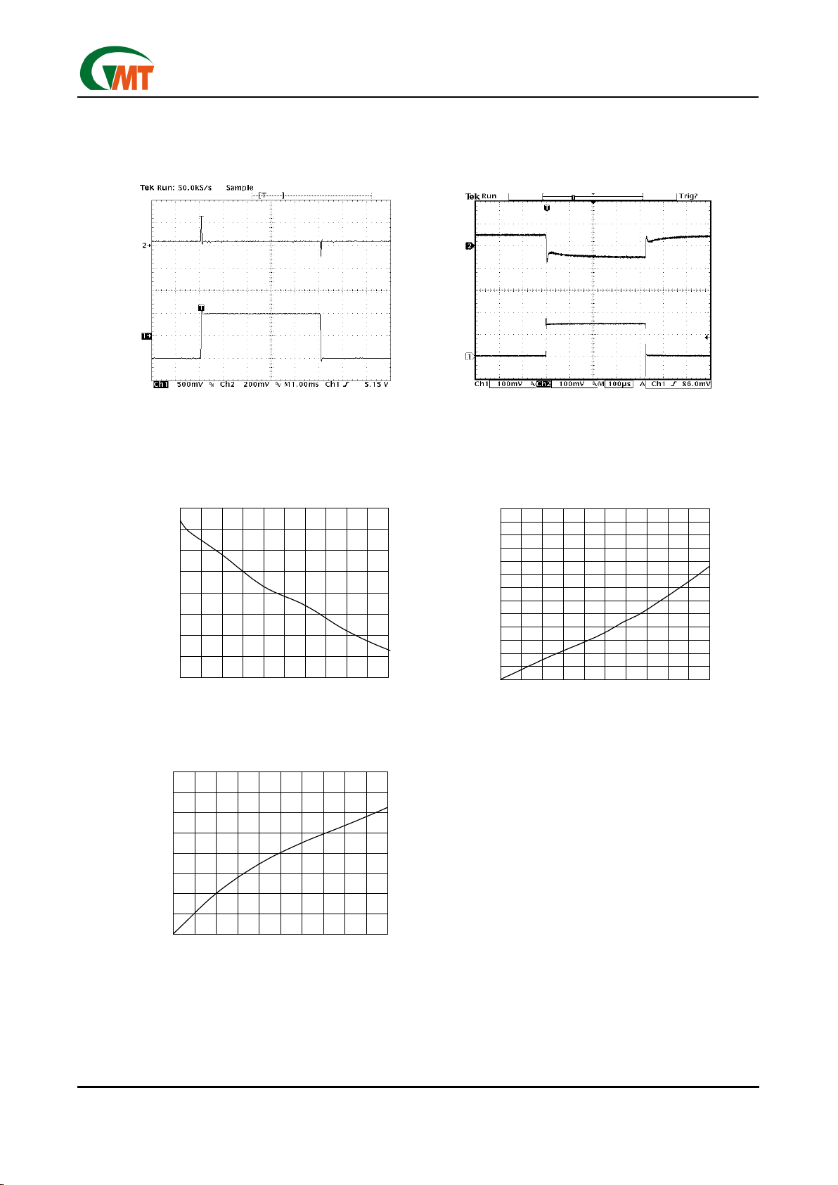
Typical Performance Characteristics
(VIN=5V , CIN=1µF, C
OUT
=10µF, TA=25°C , unless otherwise noted.)
Ch1: Vin (offset=5.00V) Ch1: Iout (400mA/div)
Ch2: Vout (offset=3.600V) Ch2: Vout (offset=3.600V)
Iout=100mA
Ground Current vs. Load Current
Line Transient Load Transient
Output Voltage vs. Load Current Dropout Voltage vs. Load Current
0
100
200
300
400
500
600
700
800
900
1000
1100
1200
1300
0 100 200 300 400 500
Load Current (mA)
Dropout Voltage (mV)
3.58
3.59
3.60
3.61
3.62
3.63
3.64
3.65
3.66
0 100 200 300 400 500
Load Current (mA)
Output Voltage (V)
0.60
0.80
1.00
1.20
1.40
1.60
1.80
2.00
2.20
0 100 200 300 400 500
Load Current (mA)
Quiescent Current (mA)
 Loading...