

GMT G905T24U, G905T24D Datasheet
Global Mixed-mode Technology Inc.
G905
2.5V 500mA Low Dropout Regulator
Features
Dropout voltage typically 0.45V @ IO = 500mA
Output current in 500mA
Output voltage accuracy +2%
Quiescent current, typically 0.6mA
Internal short circuit current limit
Internal over temperature protection
Application
CD-R/W
DVD-ROM
DVD player
LAN Switch
Broadband access
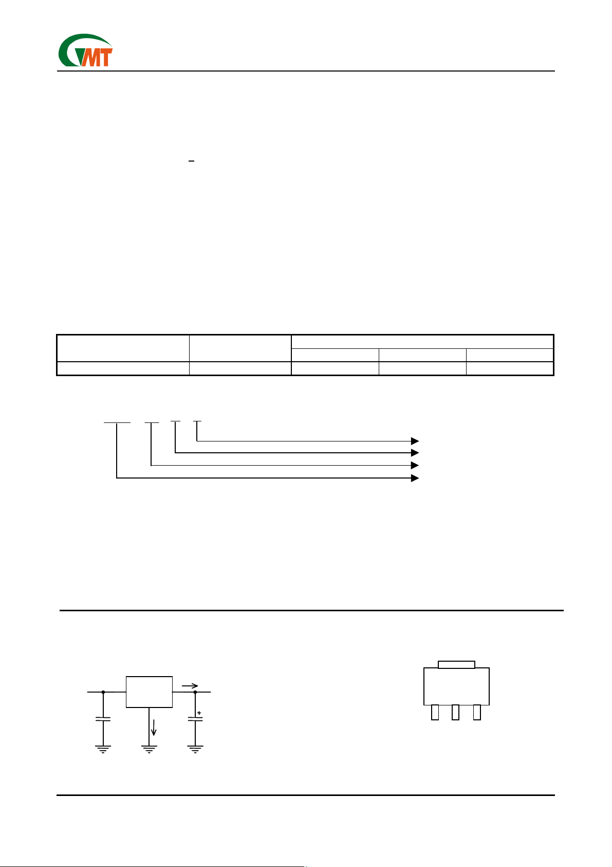
Ordering Information
ORDER NUMBER PACKAGE TYPE
G905T24U SOT 89 GND VIN V
General Description
The G905 positive 2.5V voltage regulator features the
ability to source 500mA of output current with a dropout
voltage of typically 0.45V. A low quiescent current is
provided. The typical quiescent current is 0.6mA.
Familiar regulator features such as over temperature
and over current protection circuits are provided to
prevent it from being damaged by abnormal operating
conditions.
PIN OPTION
1 2 3
OUT
Order Number Identification
GXXX XX X X
Packing Type
Pin Option
Package Type
Part Number
PACKAGE TYPE PIN OPTION PACKING
T2 : SOT 89
4 : GND V
1 2 3
V
IN
OUT
U & D : Tape & Reel Direction
Typical Application Package Type
[Note 4] : Type of C
OUT
I
I
O
V
V
IN
IN
G905
G905
O
V
V
OUT
OUT
Top View
Top View
Ver: 1.1
Jan 31, 2002
C1
C1
1µF
1µF
IQ
IQ
C
C
OUT
OUT
10µF
10µF
1
2
2
3
1
1
SOT 89
SOT 89
3
TEL: 886-3-5788833
http://www.gmt.com.tw
Global Mixed-mode Technology Inc.
Absolute Maximum Ratings
Input Voltage…………………………………………...7V
Power Dissipation Internally Limited……….…...(Note2)
Maximum Junction Temperature…………………150°C
Storage Temperature Range..……-65°C ≤ T
Lead Temperature, Time for Wave Soldering
SOT-89 Package……….……………….…...260°C, 10s
Continuous Power Dissipation (T
SOT-89
Note (1): See Recommended Minimum Footprint
(1)
……………..……………………..……...0.5W
=+25°C)
A
(Note 1)
≤+150°C
J
G905
Operating Conditions
Input Voltage…………………………..………2.7V ~ 6V
Temperature Range…………………...0°C ≤ T
(Note 1)
≤125°C
J
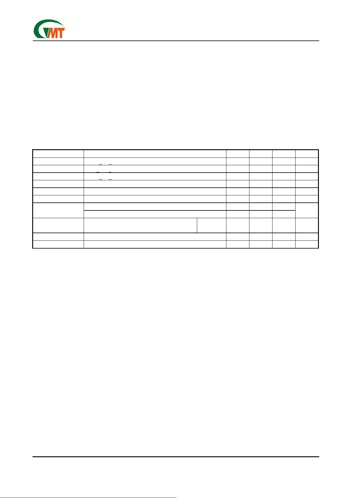
Electrical Characteristics
VIN =5V, IO = 500mA, CIN=1µF, C
=10µF. All specifications apply for TA = TJ = 25°C. [Note 3]
OUT
PARAMETER CONDITIONS MIN TYP MAX UNITS
Output Voltage 10mA < IO <500mA 2.45 2.5 2.55 V
Line Regulation 3.3V < VIN <6.5V, IO = 10mA 1 50 mV
Load Regulation 10mA < IO < 500mA 20 60 mV
Output Impedance 200mA DC and 100mA AC, fO = 120Hz 80 mΩ
Quiescent Current VIN = 5V 0.6 mA
Ripple Rejection fi = 120Hz, V
Dropout Voltage
Output Current
Short Circuit Current 0.77 A
Over Temperature 150 °C
Note 1:
Absolute Maximum Ratings are limits beyond which damage to the device may occur. Operating
IO = 500mA 450
I
= 100mA 220
O
Continuous Test, V
= 25°C, TJ < 125°C, V
T
A
ripple
=2V
, Io = 100mA 46 dB
P-P
= 3.3V
IN
within ±2% (Note 3)
OUT
Minimum
footprint
500 mA
mV
Conditions are conditions under which the device functions but the specifications might not be guaranteed. For
guaranteed specifications and test conditions see the Electrical Characteristics.
Note 2:
The maximum power dissipation is a function of the maximum junction temperature, T
sistance,
perature is T
will go into thermal shutdown. For the G905 in SOT-89 (T2) package,
, and ambient temperature TA. The maximum allowable power dissipation at any ambient tem-
θ
JA
/
. If this dissipation is exceeded, the die temperature will rise above 150°C and IC
jmax-TA
θ
JA
is 250°C/W (See recommend
θ
JA
; total thermal re-
Jmax
minimum footprint). The safe operation in SOT-89 package, it can see “Typical Performance Characteristics” (Safe Operating Area).
Note3:
Low duty pulse techniques are used during test to maintain junction temperature as close to ambient as possible.
Note4:
The type of output capacitor should be tantalum or aluminum.
Definitions
Dropout Voltage
The input/output Voltage differential at which the regulator output no longer maintains regulation against
further reductions in input voltage. Measured when the
output drops 100mV below its nominal value, dropout
voltage is affected by junction temperature, load current and minimum input supply requirements.
Load Regulation
The change in output voltage for a change in load
current at constant chip temperature. The measurement is made under conditions of low dissipation or by
using pulse techniques such that average chip temperature is not significantly affected.
Maximum Power Dissipation
The maximum total device dissipation for which the
Line Regulation
The change in output voltage for a change in input
voltage. The measurement is made under conditions
of low dissipation or by using pulse techniques such
that average chip temperature is not significantly af-
regulator will operate within specifications.
Quiescent Bias Current
Current which is used to operate the regulator chip
and is not delivered to the load.
fected.
Ver: 1.1
Jan 31, 2002
2
TEL: 886-3-5788833
http://www.gmt.com.tw
 Loading...