GMT G606 Datasheet

Ver 0.2 Preliminary
Jul 26, 2002
TEL: 886-3-5788833
http://www.gmt.com.tw
1
G606
Global Mixed-mode Technology Inc.
Smart high-current Power Switch
Features
Ultra low Ron MOSFET only 33m
ΩΩΩΩ
Continuous 6A current power switch
VCC Input voltage from 7V to 30V
MOSFET input voltage 2V to 20V
Programmable soft start for MOSFET turn on
Very low quiescent current only 180µA at V
CC
=
20V
Switch off current only 1µA
Small, 8-Pin SOP Package
Applications
Desktop and Notebook Computers
Smart Battery Packs
LAN Servers
Industrial Controls
Central Office Telecom Equipment
General Description
The G606 is a high-current power switch with logiclevel compatible on/off control. The G606 has built in a
power N-channel MOSFET, which can handle 6A continuous current, with 33mΩ on-resistance. The
drain-to-source voltage rating of the MOSFET is 20V.
The MOSFET can be turned on and off with a TTL
logic level control signal, which is applied to the
ON/OFF pin of G606. The VCC input voltage range of
G606 is from 7V to 30V. Thus, it is possible to operate
G606 directly from the adaptor or battery for the notebook applications. To tailor the turn-on time of the
MOSFET, G606 provides a SST (soft start) pin to limit
the surge current. By choosing an appropriate capacitance value, the turn-on surge current can be adjusted
The G606 is available in a small, 8-pin SOP surface-mount package.
Ordering Information
PART* TEMP. RANGE PIN-PACKAGE
G606 -40°C to +85°C 8-SOP
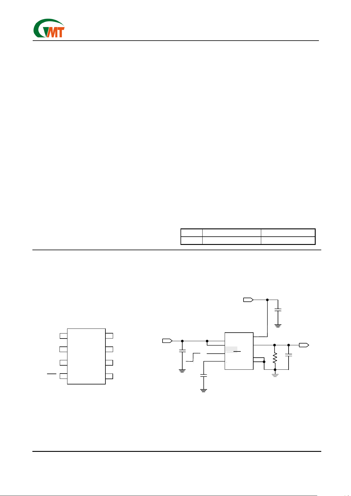
Pin Configuration Typical Operating Circuit
VCC
8
6
5
1
2
3
4
SW_S
SST
GND
8Pin SOP
G606
7
GND
SW_D
SW_D
ON/OFF
C
OUT
0.1µF
R
L
C
IN
0.1µF
U1 G606
2
3
5
4
6
7
8
1
SW_S
VCC
GND
GND
SW_D
SW_D SW_S
C
BYP
0.1µF
C
SST
0.1µF
V
IN
V
OUT
V
CC
OFF
ON
G606
ON
OFF
SST
7~30V
0~7V
ON/OFF
VCC
8
6
5
1
2
3
4
SW_S
SST
GND
8Pin SOP
G606
7
GND
SW_D
SW_D
ON/OFF
VCC
8
6
5
1
2
3
4
SW_S
SST
GND
8Pin SOP
G606
7
GND
SW_D
SW_D
ON/OFF
VCC
8
6
5
1
2
3
4
SW_S
SST
GND
8Pin SOP
G606
7
GND
SW_D
SW_D
ON/OFF
C
OUT
0.1µF
R
L
C
IN
0.1µF
U1 G606
2
3
5
4
6
7
8
1
SW_S
VCC
GND
GND
SW_D
SW_D SW_S
C
BYP
0.1µF
C
SST
0.1µF
V
IN
V
OUT
V
CC
OFF
ON
G606
ON
OFF
SST
7~30V
0~7V
ON/OFF

Ver 0.2 Preliminary
Jul 26, 2002
TEL: 886-3-5788833
http://www.gmt.com.tw
2
G606
Global Mixed-mode Technology Inc.
Absolute Maximum Ratings
VCC.to GND..…………………..….……....…-0.3V to +40V
V
SW-D
to V
SW-S
……………………..….….…..-0.3V to +25V
ON/
OFF
to GND……….…......………..…….–0.7V to +7V
Output Short-Circuit Duration……….……….……..Infinite
V
SST
to GND…………………………...…….-0.3V to +15V
Junction Temperature………………………….…..+150°C
Continuous Power Dissipation (T
A
=+25°C)
SOP-8…………………………………………………..1.0W
θ
JA
(1)
……………………………….…………..125°C /Watt
Note
(1)
: See Recommended Minimum Footprint
Recommend Operating Conditions
Supply Voltage (VCC)…………….………...+7V to +30V
Switch Input Voltage (V
SW-D
)………………+0V to +20V
Operating Temperature Range ……….-40°C to +85°C
Storage Temperature Range…………-65°C to +160°C
ESD Rating………………………….…..…………….2kV
Electrical Characteristics
(VCC= 15V, C
BYP
, CIN, C
SST
, C
OUT
= 0.1µF, TA=25°C, unless otherwise noted.) (Note1)
PARAMETER SYMBOL CONDITIONS MIN TYP MAX UNITS
I
CC_ON
Switch on, V
ON/
OFF
= 5V, No Load
53
VCC Input Supply Current
I
CC_OFF
Switch off, V
ON/
OFF
= 0V, No Load
0.053
µA
VIH Switch into on status 3.1
ON/
OFF
Input Enable Threshold
V
IL
Switch into off status 3.0
V
IIH
V
ON/
OFF
= 5V
7
ON/
OFF
Input Enable Current
I
IL
V
CC
= 15V
V
ON/
OFF
= 0V
7
nA
VCC ≤ 14.6V
V
CC
-0.06
V
ON/
OFF
= 5V
V
CC
> 14.6V 14.4
SST Voltage V
SST
V
ON/
OFF
= 0V
7V ≤ V
CC
≤
30V
0.007 0.1
V
VCC = 15V, V
SW-D
= 5V, I
OUT
= 6A 34
Switch Resistance R
DS (on)
V
CC
= 15V, V
SW-D
= 3.3V, I
OUT
= 6A 33
mΩ
V
SW-D
= 5V 2
Output turn-on rise time tr
V
SW-D
= 3.3V 1.4
V
SW-D
= 5V 0.7
Output turn-off fall time tf
V
SW-D
= 3.3V 0.8
V
SW-D
= 5V 2.7
ton
V
SW-D
= 3.3V 2.5
ms
V
SW-D
= 5V 4
Propagation Delay Time
t
off
C
SST
= 0.1µF, C
OUT
= 0.1µF
V
CC
= 12V, I
OUT
= 6A
(See Note 2)
V
SW-D
= 3.3V 3
µs
Note 1: Limits is 100% production tested at TA=25°C. Low duty pulse technique are used during test to maintain
junction temperature as close to ambient as possible.
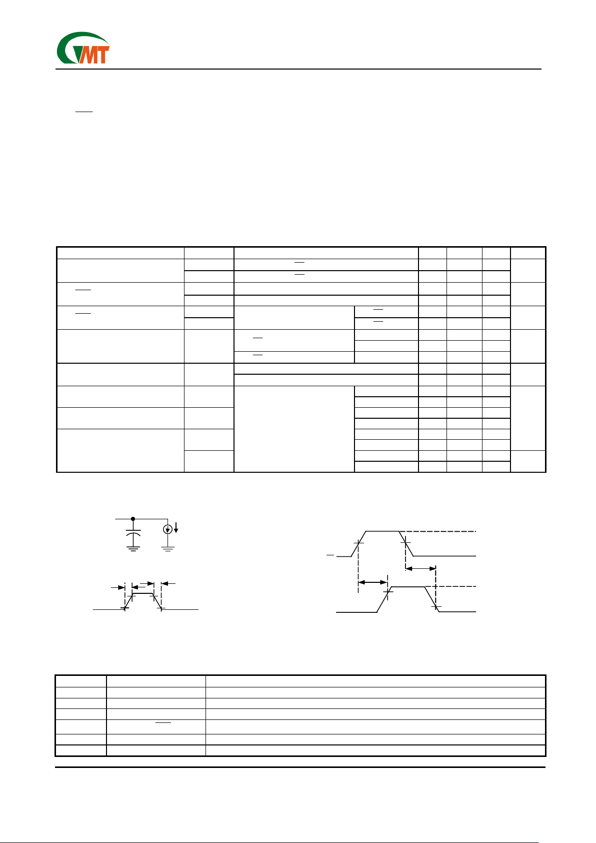
Note 2: Output rise/fall time & propagation delay time test waveform.
Test Circuits and Voltage Waveforms
Pin Description
PIN NO. PIN NAME PIN FUNCTION
1 SW_S Switch Output pin.
2 SST Adjust soft start slope of gate.
3 VCC Battery voltage input.
4
ON/
OFF
Control switch on or off.
5,6 GND Ground pin.
7,8 SW_D Switch input pin.
V
OUT
I
OUT
C
L
90%
10%
t
r
t
f
GND
Rise/Fall Time (V
OUT
)
V
OUT
V
DD
GND
50%
90%
t
off
t
on
10%
V
IN
GND
V
OUT
Voltage Waveforms
50%
Load Circuit
V
ON/OFF
V
OUT
I
OUT
C
L
90%
10%
t
r
t
f
GND
Rise/Fall Time (V
OUT
)
V
OUT
V
DD
GND
50%
90%
t
off
t
on
10%
V
IN
GND
V
OUT
Voltage Waveforms
50%
Load Circuit
V
ON/OFF

Ver 0.2 Preliminary
Jul 26, 2002
TEL: 886-3-5788833
http://www.gmt.com.tw
3
G606
Global Mixed-mode Technology Inc.
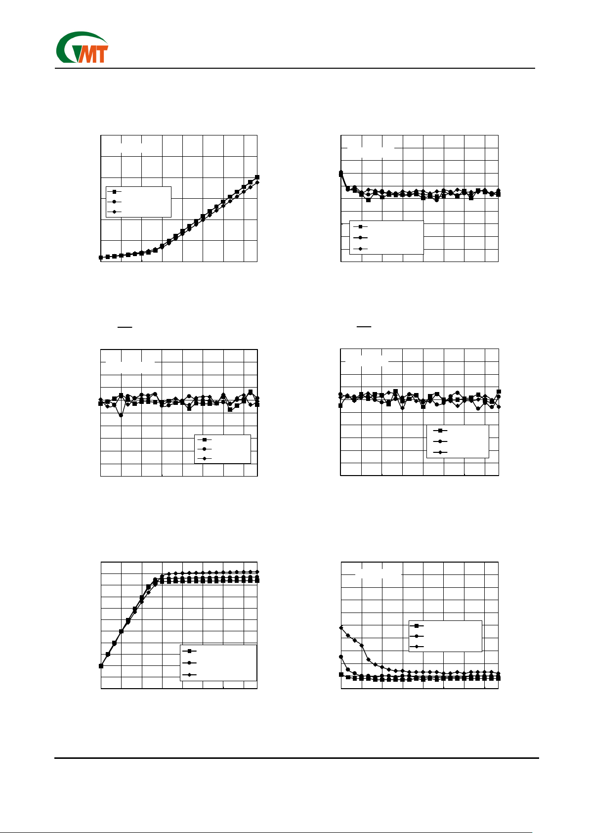
Typical Performance Characteristics
(VCC= +15V, VIN=5V, C
BYP
, CIN, C
SST
, C
OUT
= 0.1µF, TA=25°C, unless otherwise noted.)
Input Supply Current I
CC_ON
vs. V
CC
Input Supply Current I
CC_OFF
vs. V
CC
SST High Level (V
SST_HIGH
) vs. V
CC
SST Low Level (V
SST_LOW
) vs. V
CC
ON/OFF Input Enable Current (IIL) vs. V
CC
ON/OFF Input Enable Current (IIH) vs. V
CC
0
100
200
300
400
500
600
7 1013161922 2528
Vcc Input Voltage (V)
Input Supply Current I
CC_ON
(µA)
ICC_ON @TA=-40
℃
ICC_ON @TA=25
℃
ICC_ON @TA=85
℃
-1.00
-0.80
-0.60
-0.40
-0.20
0.00
0.20
0.40
0.60
0.80
1.00
7 101316192225 28
Vcc Input Voltage (V)
Input Supply Current I
CC_OFF
(µA)
ICC_OFF @ TA= -40
℃
ICC_OFF @ TA= 25
℃
ICC_OFF @ TA= 85
℃
V
ON/OFF
=5V
V
ON/OFF
=0V
-10
-8
-6
-4
-2
0
2
4
6
8
10
7 1013 1619222528
Vcc Input Voltage (V)
ON/OFF Input Enable Current I
IH
(nA)
IIH @ TA=-40
℃
IIH @ TA= 25
℃
IIH @ TA= 85
℃
V
ON/OFF
=5V
-10
-8
-6
-4
-2
0
2
4
6
8
10
7 10131619222528
Vcc Input Voltage (V)
ON/OFF Input Enable Current I
IL
(nA)
IIL @ TA=-40
℃
IIL @ TA= 25
℃
IIL @ TA= 85
℃
V
ON/OFF
=0V
5
6
7
8
9
10
11
12
13
14
15
16
7 10131619222528
V
CC
Input Voltage
SST High Level Voltage V
SST_HIGH
(V)
VSST_HIGH @ TA=-40
℃
VSST_HIGH @ TA=25
℃
VSST_HIGH @ TA=85
℃
0.00
0.01
0.02
0.03
0.04
0.05
0.06
0.07
0.08
0.09
0.10
7 10131619222528
Input Voltage VCC (V)
SST Low Level Voltage V
SST_LOW
(V)
VSST_LOW @ TA=-40
℃
VSST_LOW @ TA=25
℃
VSST_LOW @ TA=85
℃
V
ON/OFF
=0V
 Loading...