

GMT G525A2, G525A1 Datasheet
Global Mixed-mode Technology Inc.
G525A
USB High-Side Power Switch Advance Information
Features
Typical 110m
5.0V
1A minimum continuous load current
3.0V to 5.5V operating range
100 µA typical on-state supply current
1 µA typical standby supply current
Output can be forced higher than input when
operating in off state.
1.4A Typical current limit
Thermal shutdown protection
2.4V typical under-voltage lockout (UVLO)
Open-drain fault flag pin
Slow turn-on (soft-start) and fast turnoff
Logic level enable pin, available with active-
high or active-low version
UL Approved_#E232223
, Low MOSFET on resistance, at
ΩΩΩΩ
Applications
High-side power protection switch
USB power management
USB host and self-powered hubs
USB Bus-powered hubs
Hot plug-in power supplies
Battery-charger circuits
General Description
The G525A is an integrated high-side power switch
optimized for self-powered and bus-powered Universal
Serial Bus (USB) applications.
The G525A satisfies the USB standards. The switch's
low on-resistance meets USB voltage drop requirements. When the output load exceeds current-limit
threshold, G525A switches into constant mode and
limit the output current to a safe level, which is typically
1.4A, well below the UL 25VA safety requirements. An
open-drain flag output is also available to indicate fault
conditions to the local USB controller. Soft start eliminates the momentary voltage drop on the upstream port
that may occur when the switch is enabled in
bus-powered applications.
Besides, a thermal shutdown circuit is included to prevent catastrophic switch failure caused by increasing
power dissipation when continuous heavy loads or
short circuit occurs. A under-voltage lockout (UVLO)
circuit ensures that the device remains off unless there
is a valid input voltage present, and an enable input
that is compatible with both 3.3V and 5V logic.
The G525A is a UL recognized component and is
available in active-high and active-low versions in 8-pin
SOP packages.
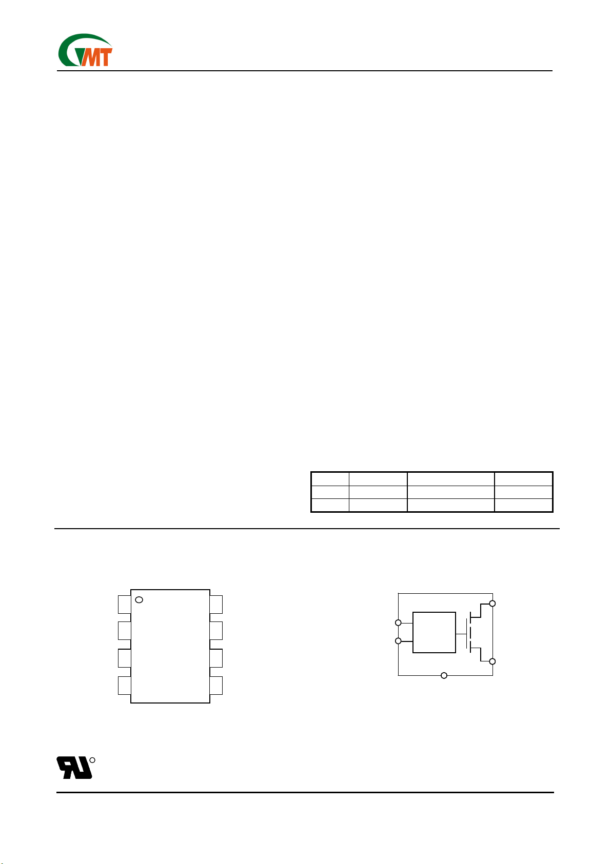
Pin Configuration
G525A
G525A
1
1
EN
EN
2
2
FLG
FLG
3
3
GND
GND
NC
NC
4
4
8 Pin SOP
8 Pin SOP
Ordering Information
PART ENABLE TEMP. RANGE PACKAGE
G525A1 Active High
G525A2 Active Low
8
8
OUT
OUT
(EN)1
IN
IN
7
7
6
6
OUT
OUT
5
5
NC
NC
(EN)1
(FLG)2
(FLG)2
-40°C to +85°C
-40°C to +85°C
G525A
G525A
Gate
Gate
Control
Control
3 (GND)
3 (GND)
8 Pin Function Block
8 Pin Function Block
8-Pin SOP
8-Pin SOP
6,8 (OUT)
6,8 (OUT)
7 (IN)
7 (IN)
R
R
UL Recognized Component
UL Recognized Component
Ver: 1.2
Nov 11, 2002
1
TEL: 886-3-5788833
http://www.gmt.com.tw
Global Mixed-mode Technology Inc.
G525A
Absolute Maximum Ratings
Supply Voltage (VIN)..…………….….………...…..+6.0V
Fault Flag Voltage (V
Fault Flag Current (I
Output Voltage (V
Output Current (I
Enable Input (V
EN
Storage Temperature (T
)..…………..……...……..+6.0V
FLG
)……………………………50mA
FLG
)..…………………………….+6.0V
OUT
).………………….Internally Limited
OUT
)……………………………-0.3V to 6V
)….………....-65°C to +150°C
S
Operating Ratings
Supply Voltage (VIN).……………………….+3V to +5.5V
Operating Temperature (T
Thermal Resistance
SOIC (
)……………………………………160°C/W
θ
JA
)…………….-40°C to +85°C
A
Lead Temperature (Soldering 5 sec.)……………260°C
ESD protection*………………..…………….……….2kV
Electrical Characteristics
(VIN=+5V; TA=25°C.)
PARAMETER CONDITION MIN TYP MAX UNITS
switch off, OUT = open 1 5 µA
IN Supply Current
EN Enable Threshold
EN Input Current
EN Input Capacitance 1 pF
Switch Resistance
OUT Turn-On Delay RL = 10Ω 0.03 ms
OUT Turn-On Rise Time RL = 10Ω, CL=100µF 0.5 ms
OUT Turn-Off Delay RL = 10Ω 1 20 µs
OUT Turn-Off Fall Time RL = 10Ω 1 20 µs
OUT Leakage Current 1 10 µA
Short Circuit Current Limit Enable into load 1.0 1.4 2.0 A
Circuit Limit Threshold Ramped load applied to enabled output 2.0 2.7 3.5 A
Threshold
FLG Output Resistance
FLG Off Current V
UVLO Threshold
Devices are ESD protected, however, handling precautions are recommended.
*
For the G525A1, off is ≤ 1.0 and on is ≥2.5V. For the G525A2, off is ≥ 2.5V and on is ≤ 1.0V. The enable input,
**
**
switch on, OUT = open 100 160 µA
**
low to high transition 2.5 V
high to low transition ** 0.8 V
V
= V
EN
V
= V
EN
VIN = 5V , I
V
= 3.3V , I
IN
TJ increasing 135 °C Overtemperature Shutdown
T
decreasing 125 °C
J
VIN = 5V, IL=10mA 10 25
V
= 3.3V, IL =10mA 15 40
IN
FLAG
V
= increasing 2.5 V
IN
V
= decreasing 2.3 V
IN
= 2.5V 0.01 1 µA
OH(min)
= 1.0V 0.01 1 µA
OL(max)
= 500mA 110 140 mΩ
OUT
= 500mA 130 180 mΩ
OUT
Ω
Ω
= 5V 0.01 1 µA
CTRL, has approximately 200mV of hysteresis.
Pin Description
PIN NUMBER PIN NAME PIN FUNCTION
: Logic level enable input. High input >2.4V typical.
: Active-low, open-drain output. Indicates overcurrent,
.
: Output MOSFET source, which also supplies IC's internal circuitry. Con-
: Output MOSFET drain. Typically connect to switched side of load.
2
1 EN
2 FLG
3 GND
4,5 NC Not internally connected.
7 IN
6,8 OUT
Ver: 1.2
Nov 11, 2002
Enable (input)
Low input <2.2V typical (1 for active high, 2 for active low).
Make sure EN never floating.
Open-Drain Fault Flag (Output)
thermal shutdown and UVLO.
Ground
Input Supply
nect to positive supply.
Switch Output
TEL: 886-3-5788833
http://www.gmt.com.tw
Global Mixed-mode Technology Inc.
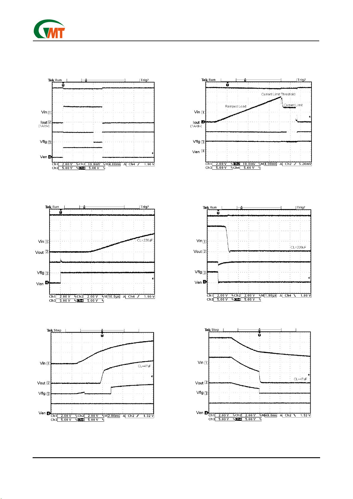
TYPICAL PERFORMANCE CHARACTERISTICS
(VIN= 5V, TA=25
C, G525A1, unless otherwise noted.)
°°°°
G525A
Flag Delay After OC
Output Turn-On Delay
Iout Ramp Chart
Output Turn-Off Delay
Ver: 1.2
Nov 11, 2002
Power Up (UVLO)
3
Power Down (UVLO)
TEL: 886-3-5788833
http://www.gmt.com.tw
 Loading...