

GMT G5173R41U Schematic [ru]
Global Mixed-mode Technology Inc.
G5173
High Efficiency, 3A Output, Synchronous Step Down
Features
Two 45mΩ (typical) MOSFETs for high effi-
ciency at 3A loads
300kHz to 2MHz Switching Frequency
0.827V±3% Voltage Reference Over Tempera-
ture
Synchronizes to External Clock
Adjustable Soft Start
UV and OV Power Good Output
Low Operating and Shutdown Quiescent Cur-
rent
Safe Start-up into Pre-Biased Output
Cycle by Cycle Current Limit, Thermal and Fre-
quency Fold Back Protection
Thermally Enhanced 3mm × 3mm 16-pin QFN
Applications
Low-Voltage, High-Density Power Systems
Point of Load Regulation for High Performance
DSPs, FPGAs, ASICs and Microprocessors
Broadband, Networking and Optical Commu-
nication Infrastructure
Ordering Information
ORDER
NUMBER
Marking
G5173R41U 5173 -40°C to +85°C TQFN3X3-16
G5173R41D 5173 -40°C to +85°C TQFN3X3-16
Note: R4: TQFN3X3-16
1: Bonding Code
U & D: Tape & Reel
TEMP.
RANGE
PACKAGE
(Green)
General Description
The G5173 device is a full featured 5.5V, 3A synchronous step down current mode converter with two integrated MOSFETs.
The G5173 enables small designs by integrating the
MOSFETs, implementing current mode control to reduce external component count, reducing inductor size
by enabling up to 2MHz switching frequency, and
minimizing the IC footprint with a small 3mm x 3mm
thermally enhanced QFN package.
The G5173 provides accurate regulation for a variety
of loads with an accurate ±3% Voltage Reference
(VREF) over temperature.
Efficiency is maximized through the integrated 45mΩ
MOSFETs and 350µA typical supply current. Using the
enable pin, shutdown supply current is reduced to 2µA
by entering a shutdown mode.
Under voltage lockout is internally set at 2.6V, but can
be increased by programming the threshold with a
resistor network on the enable pin. The output voltage
startup ramp is controlled by the soft start pin. An open
drain power good signal indicates the output is within
93% to 107% of its nominal voltage.
Frequency fold back and thermal shutdown protects
the device during an over-current condition.
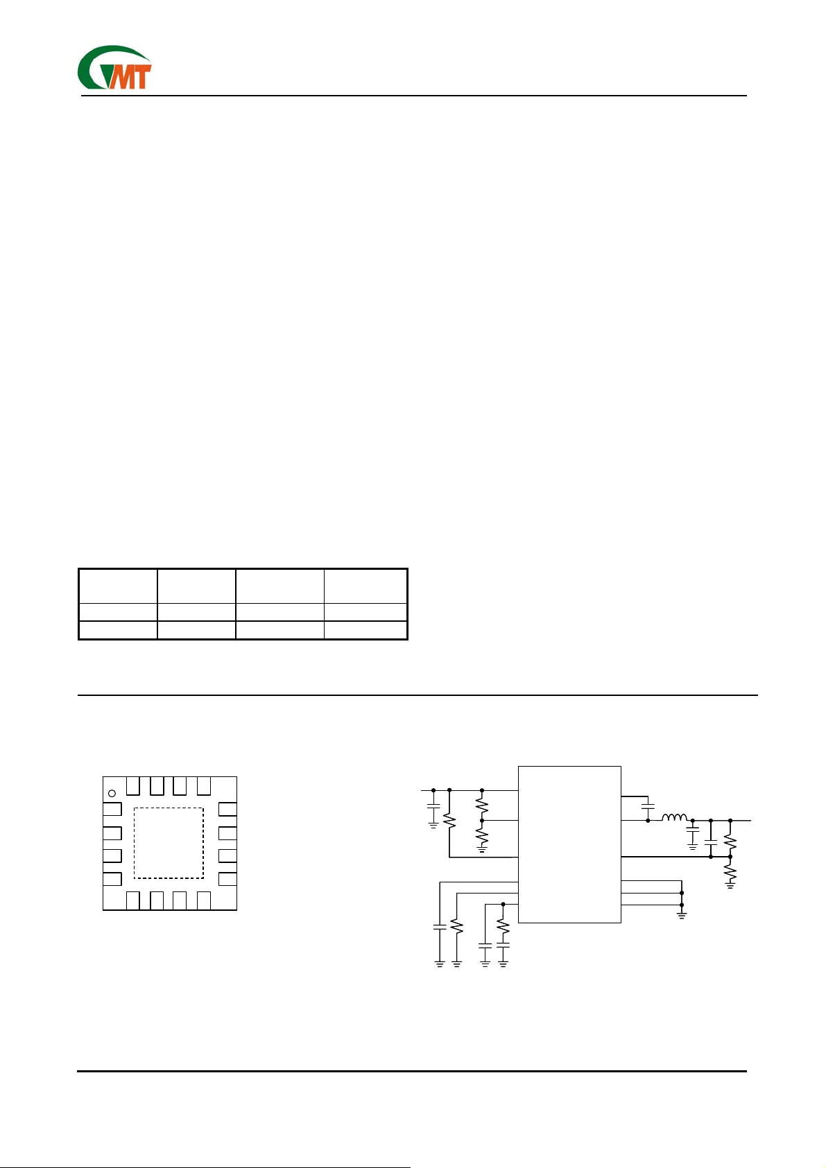
Pin Configuration Typical Application Circuit
VINA
VINA
VIN
VIN
GND
GND
GND
GND
Note: Recommend connecting the Thermal Pad to
Note: Recommend connecting the Thermal Pad to
VIN
VIN
EN
EN
15
15
16
16
1
1
2
2
3
3
4
4
the Ground for excellent power dissipation.
the Ground for excellent power dissipation.
Thermal
Thermal
Pad
Pad
5
5
6
6
FB
FB
AGND
AGND
G5173 TQFN3X3-16
G5173 TQFN3X3-16
Ver: 0.5
Nov 17, 2010
PG
PG
14
14
7
7
COMP
COMP
BS
BS
13
13
12
LX
12
LX
LX
LX
11
11
LX
LX
10
10
9
9
SS
SS
8
8
RT
RT
VIN
VIN
3.3V to 5.5V
3.3V to 5.5V
R5
C
C
I
I
10µF
10µF
0.01µF
0.01µF
* Option
* Option
* VINA must connect to VIN
* VINA must connect to VIN
R5
100KΩ
100KΩ
R
R
T
T
182KΩ
182KΩ
C
C
SS
SS
CZ*
CZ*
R3
R3
48.7KΩ
48.7KΩ
R4
R4
32.4KΩ
32.4KΩ
R
R
C
C
20KΩ
20KΩ
C
C
470PF
470PF
VINA
VINA
VIN
VIN
EN
EN
PG
PG
SS
SS
RT
RT
COMP
COMP
C
C
G5173
G5173
BS
BS
LX
LX
(0.827V)
(0.827V)
GND
GND
AGND
AGND
EP
EP
L
L
O
1.0µH
1.0µH
C
C
O
O
22*2µF
22*2µF
O
C
C
BS
BS
0.1µF
0.1µF
FB
FB
TEL: 886-3-5788833
VOUT
VOUT
1.8V
1.8V
*
*
C
C
D
D
R1
R1
100KΩ
100KΩ
R2
R2
80KΩ
80KΩ
http://www.gmt.com.tw
1

 Loading...