GMT G5111T12, G5111T11 Datasheet

Ver: 1.1
Oct 02, 2002
TEL: 886-3-5788833
http://www.gmt.com.tw
1
G5111
Global Mixed-mode Technology Inc.
Micro-power Step-Up DC/DC Converters in SOT23-5
Features
Configurable Output Voltage Up to 28V
20µA Quiescent Current
<1µA Shutdown Current
<1µA Shutdown Pin Current
Supply Range from 2.5V to 6.5V
Low V
DS(on)
: 250mV (ISW=300mA)
Tiny SOT23-5 Package
Applications
STN/TFT LCD Bias
Personal Digital Assistants (PDAs)
Handheld Computers
Digital Still Cameras
Cellular Phones
WebPad
White LED Driver
Local 3V to 5V Conversion
General Description
The G5111 boost converter is designed for small/ medium size LCD panel of high bias voltage.
Due to a typical 20µA quiescent current and 2.5V~
6.5V supply voltage range, it is suitable for battery
powered portable applications. Such as PDAs and
Handheld Computers. When the IC sets to shutdown
mode, it only consumes less than 1µA.
Furthermore, the 350mA current limit, 500ns fixed
minimum off-time and tiny SOT23-5 package facilitates the use of smaller inductor and other surface-mount components to minimize the PCB size in
those space-conscious applications.
To control the IC, no other external current is needed
for the shutdown pin. It typically consumes less than
1µA of full supply range.
Ordering Information
PART
TEMP.
RANGE
PIN-
PACKAGE
TOP MARK
G5111 T11 -40°C ~ +85°C SOT23-5 51xx
G5111 T12 -40°C ~ +85°C SOT23-5 52xx
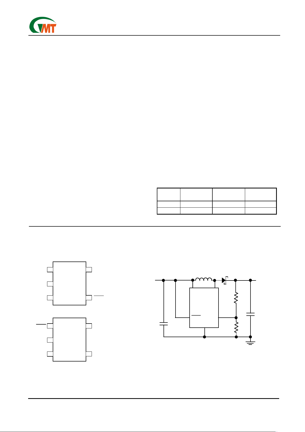
Pin Configuration Typical Application Circuit
G963
VCC
SHDN
SOT23-5
G5111 T11
5
4
1
SW
2
3
GND
FB
VCC
SW
SHDN
FB
GND
G5111
1µF
4.7µF
10µH
62k
V
IN
2.5V to 4.2V
1M
20V
12mA
G963
VCC
SHDN
SOT23-5
G5111 T12
5
4
1
SW
2
3
GND
FB
G963
VCC
SHDN
SOT23-5
G5111 T11
5
4
1
SW
2
3
GND
FB
VCC
SW
SHDN
FB
GND
G5111
1µF
4.7µF
10µH
62k
V
IN
2.5V to 4.2V
1M
20V
12mA
VCC
SW
SHDN
FB
GND
G5111
1µF
4.7µF
10µH
62k
V
IN
2.5V to 4.2V
1M
20V
12mA
G963
VCC
SHDN
SOT23-5
G5111 T12
5
4
1
SW
2
3
GND
FB

Ver: 1.1
Oct 02, 2002
TEL: 886-3-5788833
http://www.gmt.com.tw
2
G5111
Global Mixed-mode Technology Inc.
Absolute Maximum Ratings
SW to GND…………………………………..-0.3V to +30V
FB to GND…………… ………………………..-0.3V to V
CC
VCC,
SHDN
to
GND.............................….....-0.3V to +7V
Operating Temperature Range (Note 1) ..-40°C to +85°C
Junction Temperature ......….......….........….........+125°C
Storage Temperature…………........….. –65°C to +150°C
Lead Temperature (Soldering, 10 sec).…………..+300°C
Stress beyond those listed under “Absolute Maximum Rating” may cause permanent damage to the device.
Electrical Characteristics
(VCC = 3.6V,
V
SHDN
= 3.6V, TA =
25°C
)
PARAMETER CONDITIONS MIN TYP MAX UNITS
Input Voltage Range 2.5 6.5 V
Not Switching 20 30 µA
Quiescent Current
V
SHDN
= 0V
0.1 1 µA
FB Comparator Trip Point 1.18 1.2 1.22 V
Output Voltage Line Regulation 2.5V<VIN<6.5V -0.05 %/V
FB Pin Bias Current (Note 2) VFB = 1.2V 30 80 nA
V
FB
> 1V 500 ns
Switch Off Time
V
FB
< 0.6V 1.6 µs
Switch V
DS(ON)
I
SW
= 300mA 250 350 mV
Switch Current Limit 300 350 400 mA
SHDN
Pin Current
0.1 1 µA
SHDN
Input Voltage High
0.9 V
SHDN
Input Voltage Low
0.25 V
Switch Leakage Current Switch Off, VSW = 28V 0.01 5 µA
Note 1: The G5111 are guaranteed to meet performance specifications from 0°C to 85°C. Specifications over the
-40°C to 85°C operating temperature range are assured by design, characterization and correlation with statistical process controls.
Note 2: Bias current flows into the FB pin.
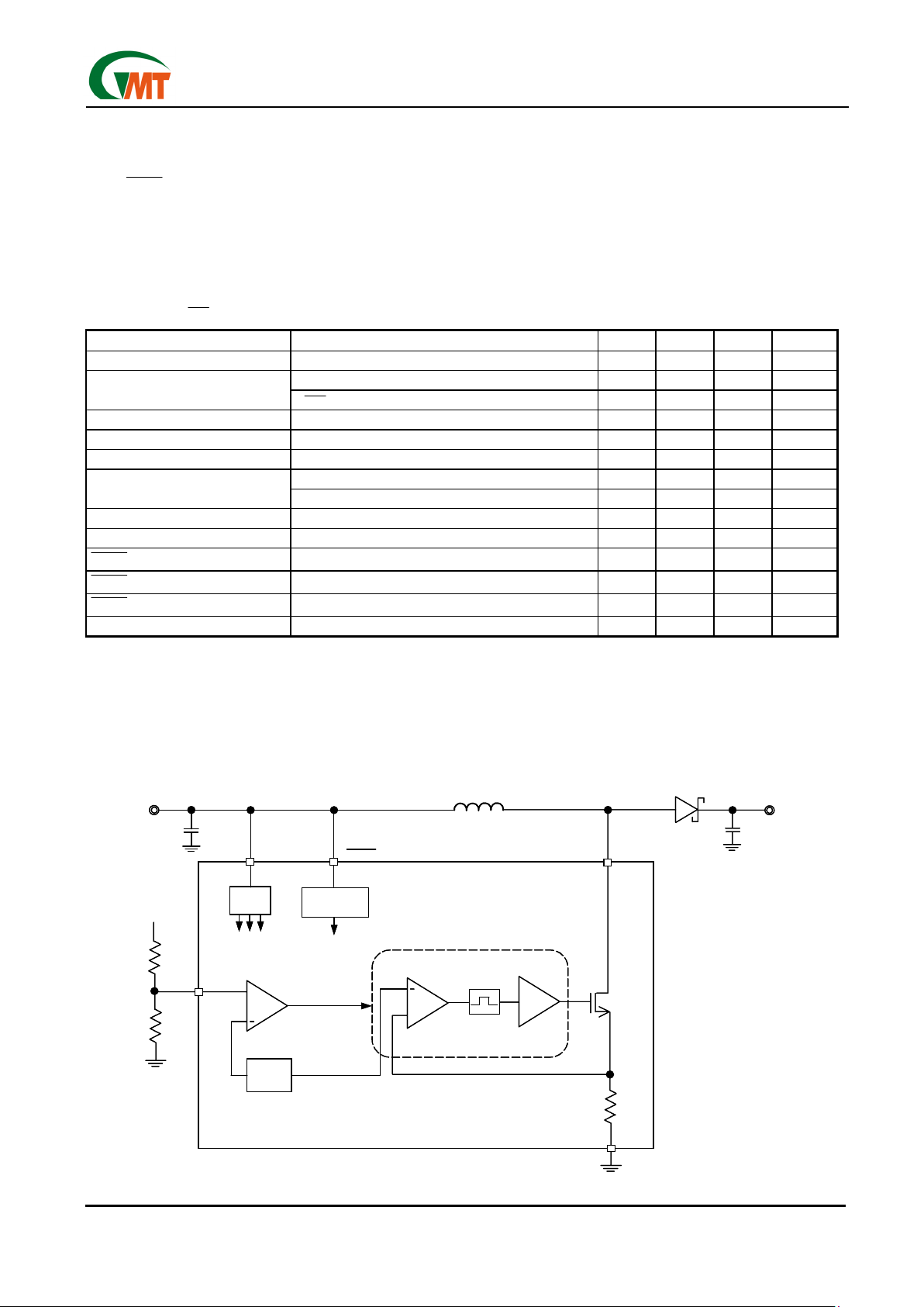
Block Diagram
+
+
VREF
BIAS
SHUTDOWN
LOGIC
C2
SW
L1
SHDN
VCC
C1
R1
R2
VOUT
FB
ERROR
COMP
1.2V
en_sw
GND
PUMP CONTROL
OC
COMP
DRIVER
T
OFF
PULSE
CONTROL
V
OUT
V
IN
+
+
VREF
BIAS
SHUTDOWN
LOGIC
C2
SW
L1
SHDN
VCC
C1
R1
R2
VOUT
FB
ERROR
COMP
1.2V
en_sw
GND
PUMP CONTROL
OC
COMP
DRIVER
T
OFF
PULSE
CONTROL
V
OUT
V
IN

Ver: 1.1
Oct 02, 2002
TEL: 886-3-5788833
http://www.gmt.com.tw
3
G5111
Global Mixed-mode Technology Inc.
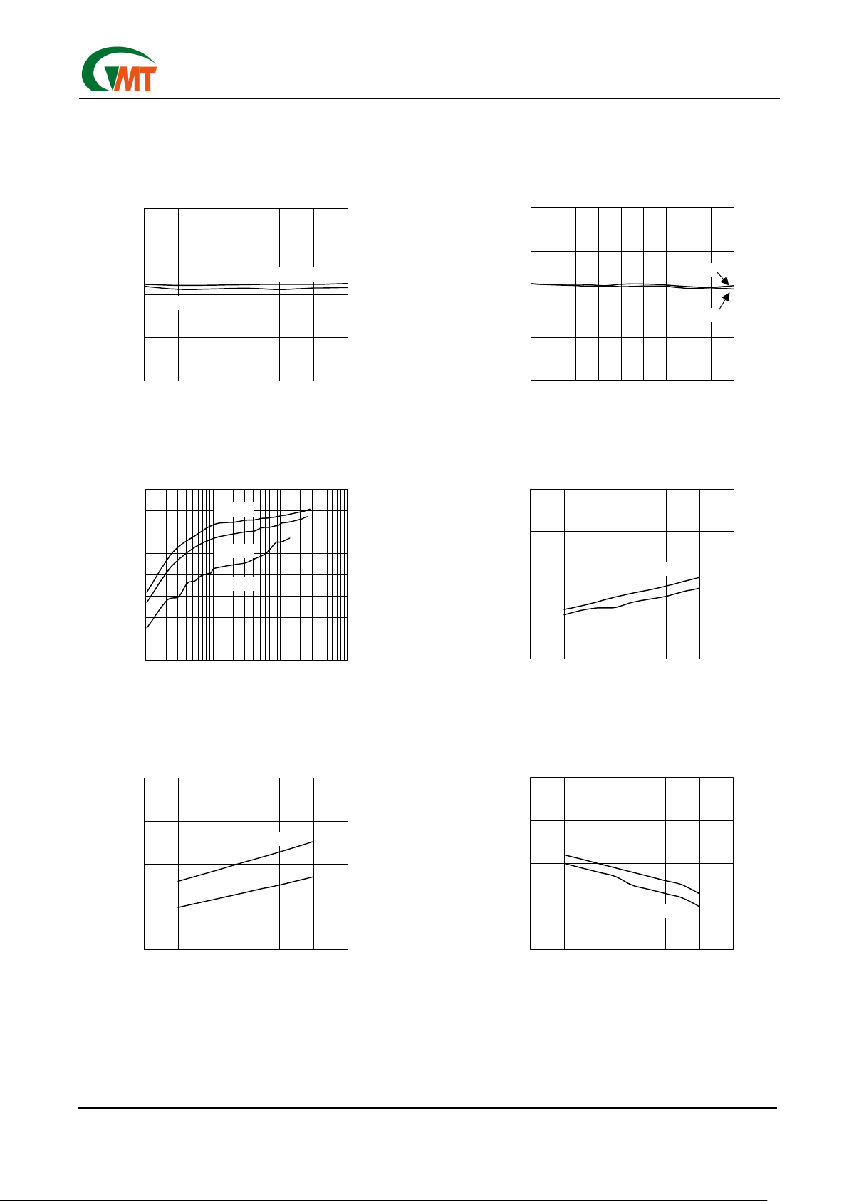
Typical Performance Characteristics
(VCC=+3.6V, V
SHDN
=+3.6V, L=10µH, TA=25°C, unless otherwise noted.)
Output Voltage vs. Input Voltage
19
19.5
20
20.5
21
2.533.544.555.5
Input Voltage (V)
Output Voltage (V)
Efficiency vs. Load Current
50
55
60
65
70
75
80
85
90
0.1 1 10 100
Load Current (mA)
Efficiency (%)
VIN=2.7V
VIN=3.6V
VIN=4.2V
Quiescent Current vs. Temperature
10
20
30
40
50
-20 0 20 40 60 80 100
Temperature (°C)
Quiescent Current (µA)
VIN=2.7V
VIN=4.2V
Vds_on vs. Temperature
100
200
300
400
500
-20 0 20 40 60 80 100
Temperature (°C)
Switch Vds_on (mV)
VIN=2.7V
VIN=4.2V
Feedback Voltage vs. Temperature
1.18
1.19
1.2
1.21
1.22
-20 0 20 40 60 80 100
Temperature (°C)
Feedback Voltage (V)
VIN=2.7V
VIN=4.2V
Output Voltage vs. Load Current
19
19.5
20
20.5
21
12345678910
Load Current (mA)
Output Voltage (V)
VIN=2.7V
VIN=4.2V
I
OUT
=1mA
I
OUT
=10mA
 Loading...