

GMT G219T-S5, G219T-D3, G219R-S5, G219R-D3 Datasheet
Ver: 1.3
Jul 19, 2002
TEL: 886-3-5788833
http://www.gmt.com.tw
1
G219
Global Mixed-mode Technology Inc.
Ultra320 Multi-mode LVD/SE SCSI Terminator
Features
Auto-selectable multi-mode Single-Ended
or LVD Termination
Meets SCSI-1, SCSI-2, SCSI-3 SPI Ultra
(Fast-20), Ultra 2(SPI-2 LVD), Ultra160 (SPI-3
LVD), and Ultra320 (SPI-4 LVD) standards
Supports active negation
3pF channel capacitance
2.9V to 5.5V operation
Thermal protection
Hot-Swap compatible
5% tolerance on SE and LVD termination
resistance
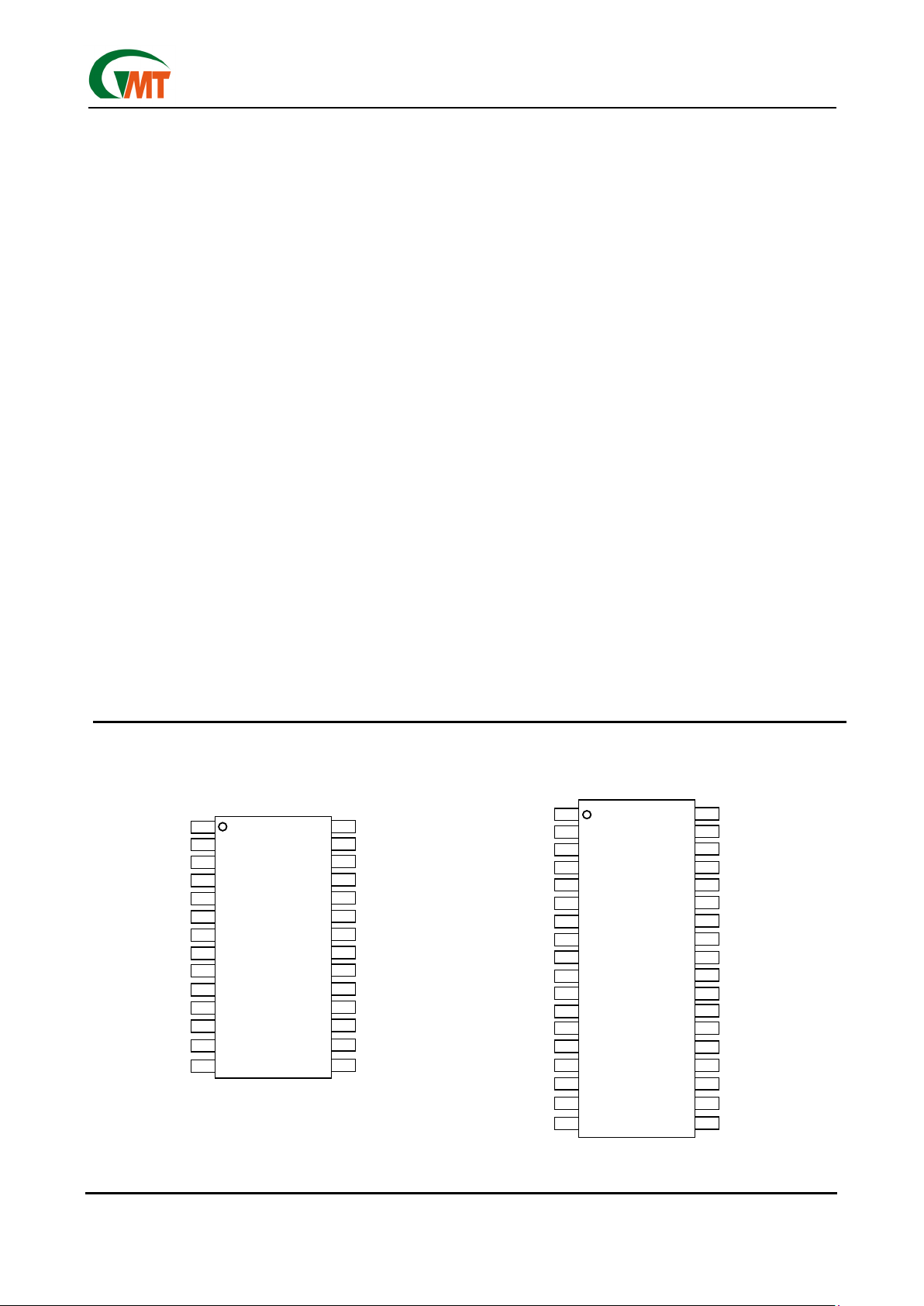
28 pin TSSOP & 36 pin SSOP package
28 Pin TSSOP: Pin Compatible with DS2119,
UCC5672
36 Pin SSOP: Pin Compatible with DS2118,
LX5241, UCC5630 and UCC5672
Applications
Server and workstation
High-end PC
Industrial PC
Disk Array (RAID)
SCSI cable
General Description
The G219 Multi-mode LVD/SE SCSI terminator provides a smooth transition into the next generation of
the SCSI Parallel Interface (SPI-4). It automatically
senses the bus, via DIFFSENS, and switches the termination to either single-ended (SE) or low voltage
differential (LVD) SCSI, dependent on which type of
devices are connected to the bus. If the G219 detects
a HVD SCSI device, it switches to a high impedance
state. For a 16-bit Wide SCSI bus to be operational,
three G219 terminators are needed.
The Multi-mode terminator contains all functions required to terminate and auto detect and switch modes
for SCSI Parallel Interface (SPI) bus architectures. For
the SE termination, one regulator and nine precision
110ohm resistors are used. For the LVD termination,
the G219 integrates 18 regulated supplies with nine
precision resistor strings.
Pin Configuration
NC
NC
R1+
R1-
R2-
HS/GND
HS/GND
R3+
R3-
R4+
R4-
R5+
R5-
DISCNCT
GND
TPWR
HVD
LVD
SE
R9-
R9+
R8-
R8+
HS/GND
HS/GND
HS/GND
R7-
R7+
R6-
R6+
DIFFB
DIFFSENSE
M/S
VREF
R2+
HS/GND
36Pin SSOP
G219
1
2
3
4
28
27
26
25
5
6
7
8
9
10
11
12
13
14
24
23
22
21
20
19
16
17
15
18
33
32
31
30
29
36
35
34
R1-
R1+
R2-
NC/ HS GND
R3+
R3-
R4+
R4-
R5+
R5-
DISCNCT
GND
TPWR
R9-
R9+
R8+
R8-
R7-
R6-
R6+
DIFFB
DIFFSENSE
M/S
28Pin TSSOP
VREF
R2+
TPWR
R7+
G219
1
2
3
4
28
27
26
25
5
6
7
8
9
10
11
12
13
14
24
23
22
21
20
19
18
17
16
15
NC/ HS GND
NC
NC
R1+
R1-
R2-
HS/GND
HS/GND
R3+
R3-
R4+
R4-
R5+
R5-
DISCNCT
GND
TPWR
HVD
LVD
SE
R9-
R9+
R8-
R8+
HS/GND
HS/GND
HS/GND
R7-
R7+
R6-
R6+
DIFFB
DIFFSENSE
M/S
VREF
R2+
HS/GND
36Pin SSOP
G219
1
2
3
4
28
27
26
25
5
6
7
8
9
10
11
12
13
14
24
23
22
21
20
19
16
17
15
18
33
32
31
30
29
36
35
34
R1-
R1+
R2-
NC/ HS GND
R3+
R3-
R4+
R4-
R5+
R5-
DISCNCT
GND
TPWR
R9-
R9+
R8+
R8-
R7-
R6-
R6+
DIFFB
DIFFSENSE
M/S
28Pin TSSOP
VREF
R2+
TPWR
R7+
G219
1
2
3
4
28
27
26
25
5
6
7
8
9
10
11
12
13
14
24
23
22
21
20
19
18
17
16
15
NC/ HS GND

Ver: 1.3
Jul 19, 2002
TEL: 886-3-5788833
http://www.gmt.com.tw
2
G219
Global Mixed-mode Technology Inc.
Ordering Information
PART NUMBER TEMP. RANGE PIN-PACKAGE FEATURE
G219T-D3 0ºC-70ºC TSSOP-28 pin / Tube DISCNCT does not disable VREF
G219R-D3 0ºC-70ºC TSSOP-28 pin / Tape & Reel DISCNCT does not disable VREF
G219T-S5 0ºC-70ºC SSOP-36 pin / Tube DISCNCT does not disable VREF
G219R-S5 0ºC-70ºC SSOP-36 pin / Tape & Reel DISCNCT does not disable VREF
Note:
DIFFSENSRefers to the SCSI bus signal.
DIFFSENSERefers to the G219 pin name and internal circuitry relating to differential sensing.
DIFFBRefers to the G219 pin name and internal circuitry relating to monitoring the DIFFSENS line.
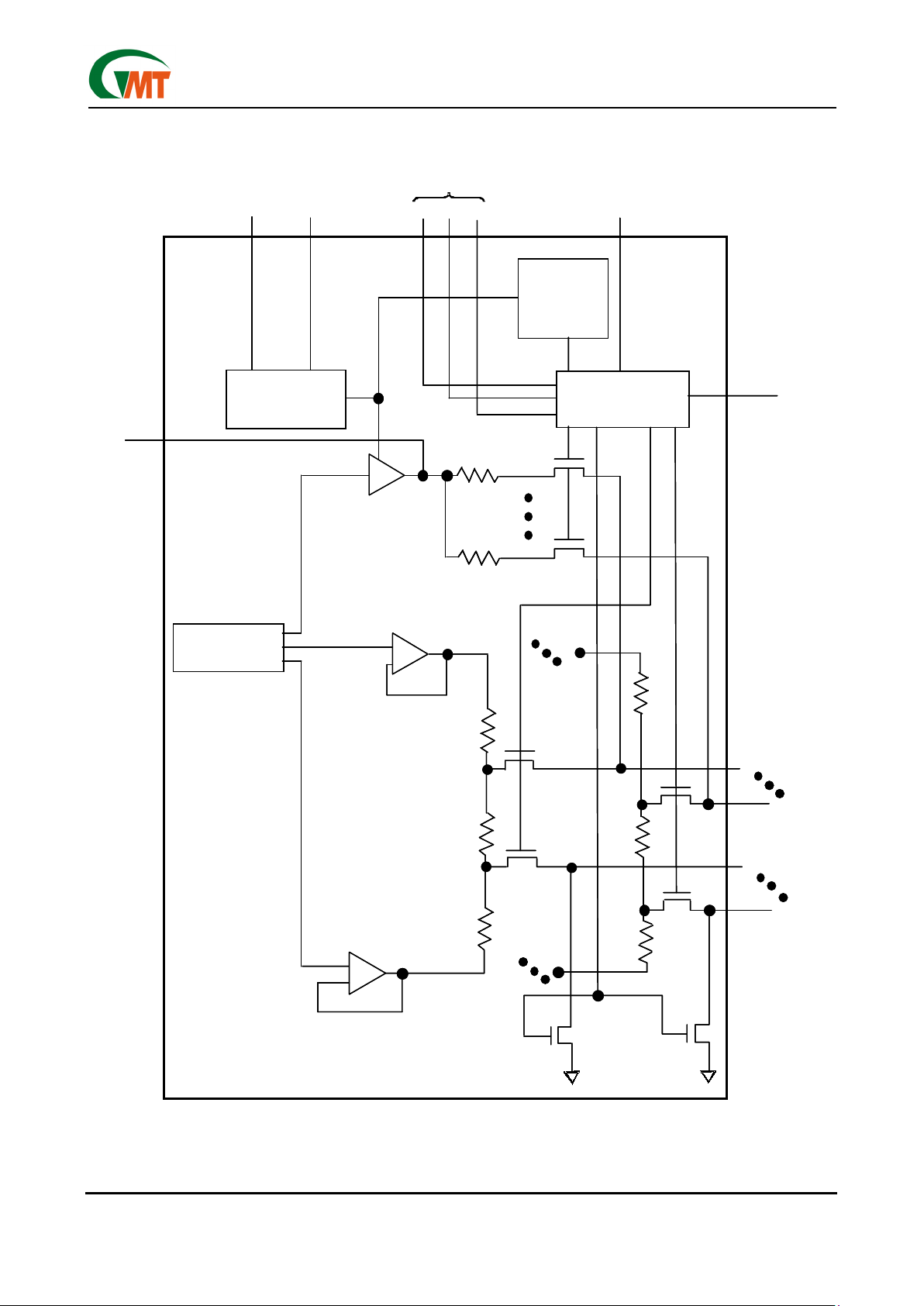
Functional Description
The G219 is used in multi-mode active termination
applications, where single ended (SE) and low voltage
differential (LVD) devices might coexist. The LVD termination section consists of 18 source/sink amplifiers
(VTOP, VBOT), biasing circuitry and nine precision
resistor strings (RTOP, RMID, RBOT). The SE termination section consists of a 2.85V source/sink regulator with 9 precision 110ohm resistor. The DIFFSENSE
section consists of a 1.3V, 5mA driver and a sensing
circuit (Figure 1)
DIFFSENS is used to identify which types of SCSI
devices are present on the bus. If the voltage on
DIFFSENS is between 0-0.5V the bus is single-ended;
if it is between 0.7-1.9V the bus is LVD; and if it is
greater than 2.4V, the bus is HVD.
The G219 DIFFB pin monitors the DIFFSENS line to
determine the proper operating mode of the device.
HVD Isolation Mode
The G219 identifies that there is
an HVD (high voltage differential) device on the SCSI
bus and isolates the termination pins from the bus.
When DISCNCT is pulled high, the termination pins
are isolated from the SCSI bus, and VREF is
grounded. During thermal shutdown, the termination
pins are isolated from the SCSI bus and VREF is
grounded. The DIFFSENSE driver is shut down during
either of these two events.
To ensure proper operation, the TPWR pin should be
connected to the SCSI bus TERMPWR line. As with all
analog circuitry, the TERMPWR lines should be bypassed locally. A 2.2µF capacitor and a 0.01µF high
frequency capacitor is recommended between TPWR
and ground and placed as close as possible to the
G219. The G219 should be placed as close as possible to the SCSI connector to minimize signal and
power trace length, thereby resulting in less input ca-
pacitance and reflections which can degrade the bus
signals.
The DIFFSENSE pin can drive the SCSI DIFFSENS
line (when M/S is pulled high) to determine the SCSI
bus operating mode. The G219 switches to the termination mode that is appropriate for the bus based on
the value of the DIFFSENS voltage. These modes are:
LVD mode
LVD termination is provided by a precision
resistor string with two amplifiers. This configuration
yields a 105Ω differential and 150Ω common mode
impedance. A fail safe bias of 112mV is maintained
when no drivers are connected to the SCSI bus.
SE mode
When the external driver for a given signal
line turns off, the active terminator will pull that signal
line to 2.85 volts (quiescent state). When used with an
active negation driver, the power amp can sink 22mA
per line while keeping the voltage reference in regulation. The terminating resistors maintain their 110Ω
value.
To maintain the specified regulation, a 4.7µF capacitor
is required between the VREF pin and ground of each
G219. A high frequency cap (0.1µF ceramic recommended) can also be placed on the VREF pin in applications that use fast rise/fall time drivers. A typical
SCSI bus configuration is shown in Figure2.
An internal pull down resistor assures that the G219
will be terminating the bus if the DISCNCT pin is left
floating.
DIFFSENS noise filtering
The G219 incorporates a internal digital filter to remove the noise signal on the DIFFSENS control line,
thereby eliminating erroneous switching between
modes. The external filter may be used in addition to
the internal digital filter.
Ver: 1.3
Jul 19, 2002
TEL: 886-3-5788833
http://www.gmt.com.tw
3
G219
Global Mixed-mode Technology Inc.
Block Diagram
(Figure 1)
DIFFB
DIFFSENSE
SE
LVD
HV D
THE RMA L
SHUTDOW N
CIRCUITRY
DISCNCT
CO NT ROL
LOGIC
VREF
DIFFSENSE
CIRCUITRY
REFERENCE
GENERAT ION
VREF
110 Ohms
110 Ohms
R1-
R9-
VTOP1
RTO P1
RMID1
RBO T1
R1+
R1-
R9-
R9+
R1-
R9-
SE
GND
DRIV ER
VBOT1
R1+
R9+
36pin SSOP only
+
_
+
_
(
)
X 9
X 9
RTO P9
RMID9
RBO T9
M/S
DIFFB
DIFFSENSE
SE
LVD
HV D
THE RMA L
SHUTDOW N
CIRCUITRY
DISCNCT
CO NT ROL
LOGIC
VREF
DIFFSENSE
CIRCUITRY
REFERENCE
GENERAT ION
VREF
110 Ohms
110 Ohms
R1-
R9-
VTOP1
RTO P1
RMID1
RBO T1
R1+
R1-
R9-
R9+
R1-
R9-
SE
GND
DRIV ER
VBOT1
R1+
R9+
36pin SSOP only
+_+
_
+_+
_
(
)
X 9
X 9
RTO P9
RMID9
RBO T9
M/S
 Loading...