

Global Mixed-mode Technology Inc.
G1421
2W Stereo Audio Amplifier With No Headphone
Coupling Capacitor Function
Features
Depop Circuitry Integrated
Output Power at 1% THD+N, VDD=5V
--1.8W/CH (typical) into a 4
--1.2W/CH (typical) into a 8
Eliminates Headphone Amplifier Output Cou-
Load
ΩΩΩΩ
Load
ΩΩΩΩ
pling Capacitors
Maximum Output Power Clamping Circuitry
Integrated
Bridge-Tied Load (BTL), Single-Ended (SE),
and Stereo Headphone Amplifier (HP-IN) modes
Supported
Stereo Input MUX
Mute and Shutdown Control Available
Surface-Mount Power Package
24-Pin TSSOP-P
Applications
Stereo Power Amplifiers for Notebooks or
Desktop Computers
Multimedia Monitors
Stereo Power Amplifiers for Portable Audio
Systems
General Description
G1421 is a stereo audio power amplifier in 24pin
TSSOP thermal pad package. It can drive 1.8W continuous RMS power into 4Ω load per channel in
Bridge-Tied Load (BTL) mode at 5V supply voltage. Its
THD is smaller than 1% under the above operation
condition. To simplify the audio system design in the
notebook application, G1421 supports the Bridge-Tied
Load (BTL) mode for driving the speakers, Single-End
(SE) mode for driving the headphone. In the HP-IN
mode, it can support a DC value to the phone-jacket
and drive the headphone without the audio amplifier
outputs coupling capacitors. G1421 can mute the
output when Mute-In is activated. For the low current
consumption applications, the SHDN mode is supported to disable G1421 when it is idle. The current
consumption can be further reduced to below 5µA.
G1421 also supports two input paths, that means two
different gain loops can be set in the same PCB and
choosing either one by setting HP/
hances the hardware designing flexibility. G1421 also
supports an extra function -- the maximum output
power clamping function to protect the speakers or
headphones from burned-out.
LINE pin. It en-
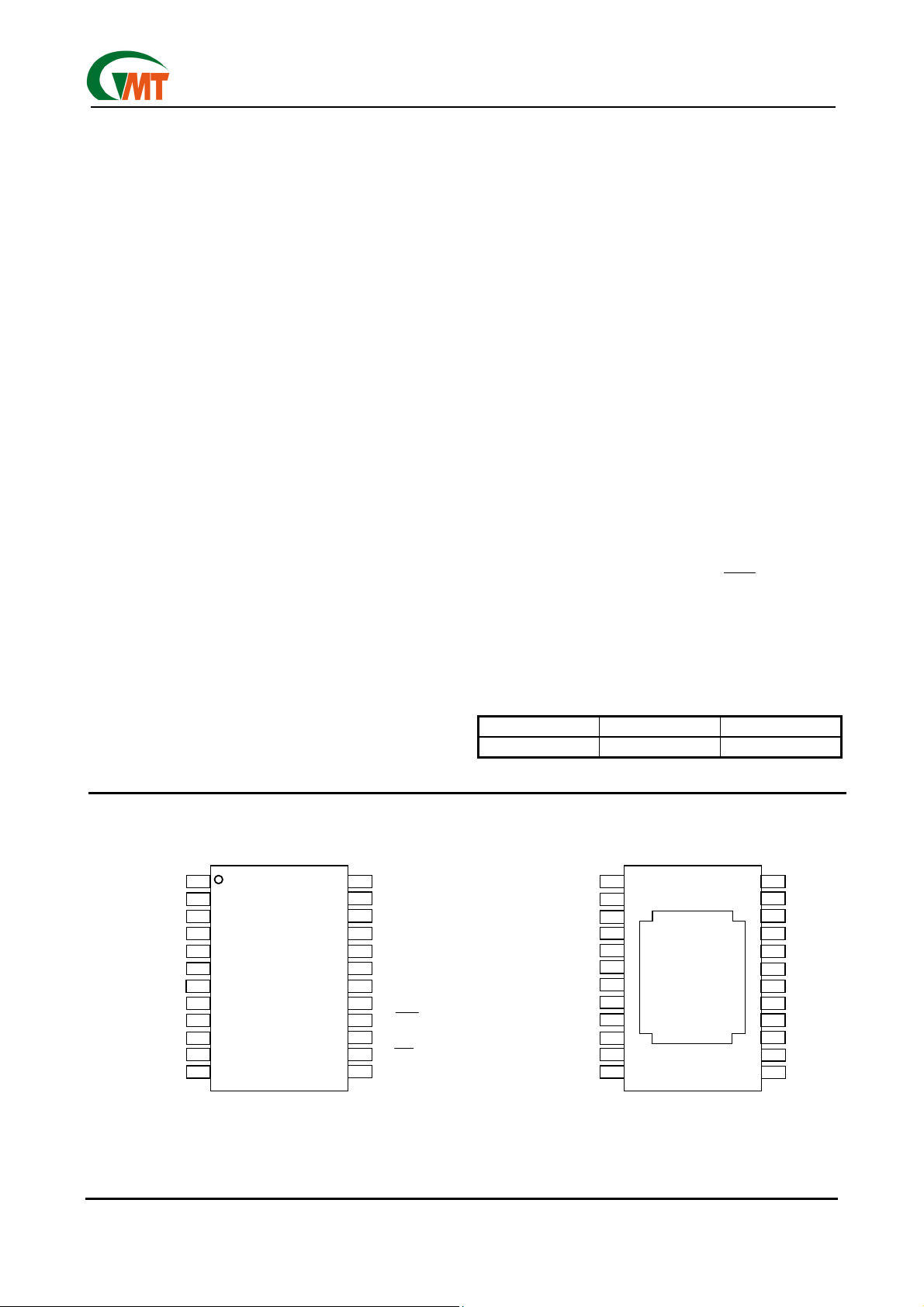
Pin Configuration
GND/HS
GND/HS
LOUT+
LOUT+
LLINEIN
LLINEIN
LHPIN
LHPIN
LBYPASS
LBYPASS
SHUTDOWN
SHUTDOWN
MUTE OUT
MUTE OUT
LOUT-
LOUT-
MUTE IN
MUTE IN
GND/HS
GND/HS
TJ
TJ
LVDD
LVDD
1
1
2
2
3
3
4
4
5
5
6
6
7
7
8
8
9
9
10
10
11
11
12
12
Ordering Information
PART NUMBER TEMP. RANGE PIN-PACKAGE
G1421 -40°C to +85°C 24 TSSOP
G1421
G1421
GND/HS
GND/HS
24
24
23
23
VOL
VOL
22
22
ROUT+
ROUT+
RLINEIN
RLINEIN
21
21
20
20
RHPIN
RHPIN
Thermal
19
19
RBYPASS
RBYPASS
RVDD
RVDD
18
18
HP-IN
HP-IN
17
17
HP/LINE
HP/LINE
16
16
ROUT-
ROUT-
15
15
SE/BTL
SE/BTL
14
14
13
13
GND/HS
GND/HS
Top View Bottom View
Top View Bottom View
24Pin TSSOP
24Pin TSSOP
Thermal
Pad
Pad
14
14
Ver: 0.7 Preliminary
Dec 20, 2002
1
TEL: 886-3-5788833
http://www.gmt.com.tw
Global Mixed-mode Technology Inc.
G1421
Pin Description
PIN NAME I/O FUNCTION
1,12,13,24 GND/HS Ground connection for circuitry, directly connected to thermal pad.
2 TJ O Source a current inversely to the junction temperature. This pin should be left uncon-
nected during normal operation. For more information, see the junction temperature
measurement section of this document.
3 LOUT+ O Left channel + output in BTL mode, + output in SE mode.
4 LLINE IN I Left channel line input, selected when HP/ pin is held low.
5 LHP IN I Left channel headphone input, selected when HP/pin is held high.
6 LBYPASS Connect to voltage divider for left channel internal mid-supply bias.
7 LVDD I Supply voltage input for left channel and for primary bias circuits.
8 SHUTDOWN I Shutdown mode control signal input, places entire IC in shutdown mode when held high,
I
= 5µA.
DD
9 MUTE OUT O Follows MUTE IN pin, provides buffered output.
10 LOUT- O Left channel - output in BTL mode, high impedance state in SE mode. Supply VDD/2 to
the phone jacket in HP-IN mode.
11 MUTE IN I Mute control signal input, hold low for normal operation, hold high to mute.
14 SE/ I Mode control signal input, hold low for BTL mode, hold high for SE mode.
15 ROUT- O Right channel - output in BTL mode, high impedance state in SE mode.
16 HP/ I MUX control input, hold high to select headphone inputs (5,20), hold low to select line
inputs (4,21).
17 HP-IN This pin can activate the HP-IN mode to supplied the VDD/2 at LOUT- onto the phone
jacket. So the DC blocking capacitors can be removed in HP-IN type (like SE mode
except no DC blocking capacitors). Hold high to activate this function. If this function is
not used, it should be strongly tied to low.
18 RVDD I Supply voltage input for right channel.
19 RBYPASS Connect to voltage divider for right channel internal mid-supply bias.
20 RHP IN I Right channel headphone input, selected when HP/pin is held high.
21 RLINE IN I Right channel line input, selected when HP/pin is held low.
22 ROUT+ O Right channel + output in BTL mode, + output in SE mode.
23 VOL I The output power can be clamped by setting a low bound voltage to this pin. The high
bound voltage will be generated internally. The output voltage will be clamped between
high/low bound voltages. Then the output power is limited. It is weakly pull-low internally, let this pin floating or tied to GND can deactivate this function.
Ver: 0.7 Preliminary
Dec 20, 2002
2
TEL: 886-3-5788833
http://www.gmt.com.tw
Global Mixed-mode Technology Inc.
Absolute Maximum Ratings
Supply Voltage, VCC…………………..…...…….……...6V
Operating Ambient Temperature Range
T
…….…………………………….……….-40°C to +85°C
A
Maximum Junction Temperature, T
Storage Temperature Range, T
Soldering Temperature, 10seconds, T
…..……….….150°C
J
….….-65°C to+150°C
STG
……….……300°C
S
Power Dissipation
T
T
T
Electrostatic Discharge, V
Human body mode
(1)
≤ 25°C…………………………………………..2.7W
A
≤ 70°C…………………………………………..1.7W
A
≤ 85°C………………….……………………….1.4W
A
ESD
G1421
Lout- pin………………………..…………-8000 to 8000V
Other pins………………………………...-3000 to 3000
Note:
(1)
: Recommended PCB Layout.
(2)
: Human body model : C = 100pF, R = 1500Ω, 3 positive pulses plus 3 negative pulses
Electrical Characteristics
DC Electrical Characteristics, TA=+25°C
PARAMETER SYMBOL CONDITIONS MIN TYP MAX UNIT
Supply Current IDD
DC Differential Output Voltage V
Supply Current in Mute Mode I
IDD in Shutdown ISD VDD = 5V 2 5 µA
VDD =3.3V HP-IN 5.5 7
VDD = 5V HP-IN 6.5 8
VDD =3.3V
V
= 5V
DD
VDD = 5V,Gain = 2 5 25 mV
O(DIFF)
VDD = 5V
DD(MUTE)
Stereo BTL 7 9
Stereo SE 3.5 5.6
Stereo BTL 8 11
Stereo SE 4 6.5
Stereo BTL 8 11
HP-IN 6.5 8
Stereo SE 4 6.5
mA
mA
(2)
(AC Operation Characteristics, VDD = 5.0V, TA=+25°C, RL = 4
PARAMETER SYMBOL CONDITIONS MIN TYP MAX UNIT
THD = 1%, BTL, RL = 4Ω 1.8
THD = 1%, BTL, RL = 8Ω 1.12
THD = 10%, BTL, RL = 4Ω 2
THD = 10%, BTL, RL = 8Ω 1.4
Output power (each channel) see Note P
Total harmonic distortion plus noise THD+N
Maximum output power bandwidth BOM G = 10, THD < 1% >20 kHz
Phase margin RL = 4Ω, Open Load 71
Power supply ripple rejection PSRR f = 120Hz 75 dB
Mute attenuation 85 dB
Channel-to-channel output separation f = 1kHz 82 dB
Line/HP input separation 80 dB
BTL attenuation in SE mode 85 dB
Input impedance ZI 2 MΩ
Signal-to-noise ratio PO = 500mW, BTL 90 dB
Output noise voltage Vn Output noise voltage 55 µV (rms)
Note :Output power is measured at the output terminals of the IC at 1kHz.
(OUT)
THD = 1%, SE, RL = 4Ω 500
THD = 1%, SE, RL = 8Ω 320
THD = 10%, SE, RL = 4Ω 650
THD = 10%, SE, RL L = 8Ω 400
THD = 0.5%, SE, R
PO = 1.6W, BTL, RL = 4Ω 500
PO = 1W, BTL, RL = 8Ω 150
PO = 75mW, SE, RL = 32Ω 20
= 1V, RL = 10KΩ, G = 1 10
V
I
, unless otherwise noted)
ΩΩΩΩ
= 32Ω 90
L
W
mW
m%
°
Ver: 0.7 Preliminary
Dec 20, 2002
3
TEL: 886-3-5788833
http://www.gmt.com.tw
Global Mixed-mode Technology Inc.
G1421
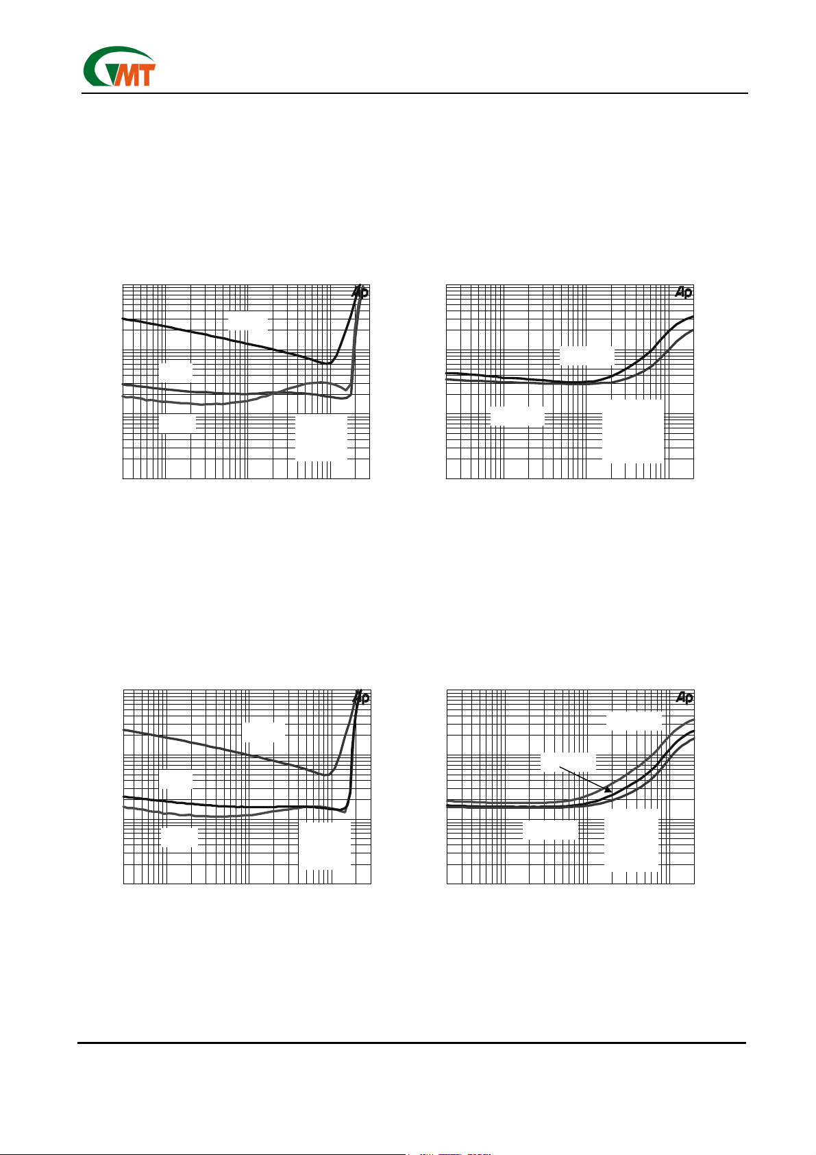
TOTAL HARAMONIC DISTORTION PLUS NOISE
vs OUTPUT POWER
10
5
2
1
0.5
%
0.2
0.1
0.05
0.02
0.01
3m 35m 10m 20m 50m 100m 200m 500m 1 2
1kHz
20 Hz
20kHz
W
VDD=5V
RL=3
Ω
BTL
TOTAL HARMONIC DISTORTION PLUS NOISE
vs OUTPUT FREQUENCY
10
5
2
1
0.5
%
0.2
0.1
0.05
0.02
0.01
20 20k50 100 200 500 1k 2k 5k 10k
Po=1.5W
Po=1.8W
Hz
VDD=5V
RL=3
Ω
BTL
Av=-2V/V
TOTAL HARAMONIC DISTORTION PLUS NOISE
vs OUTPUT POWER
10
5
2
1
0.5
%
0.2
0.1
0.05
0.02
0.01
3m 35m 10m 20m 50m 100m 200m 500m 1 2
1kHz
20 Hz
20kHz
W
VDD=5V
RL=4
Ω
BTL
TOTAL HARMONIC DISTORTION PLUS NOISE
vs OUTPUT FREQUENCY
10
5
2
1
0.5
%
0.2
0.1
0.05
0.02
0.01
20 20k50 100 200 500 1k 2k 5k 10k
Av=-2V/V
Av=-1V/V
Hz
Av=-4V/V
VDD=5V
RL=4
Ω
BTL
Po=1.5W
Ver: 0.7 Preliminary
Dec 20, 2002
TEL: 886-3-5788833
http://www.gmt.com.tw
4
Global Mixed-mode Technology Inc.
G1421
TOTAL HARAMONIC DISTORTION PLUS NOISE
vs OUTPUT FREQUENCY
10
VDD=5V
5
RL=4
Ω
BTL
2
Av=-2V/V
1
0.5
%
0.2
0.1
0.05
0.02
0.01
20 20k50 100 200 500 1k 2k 5k 10k
Po=0.25W
Hz
Po=1.5W
Po=0.75W
TOTAL HARMONIC DISTORTION PLUS NOISE
vs OUTPUT POWER
10
5
2
1
0.5
%
0.2
0.1
0.05
0.02
0.01
3m 35m 10m 20m 50m 100m 200m 500m 1 2
20kHz
1kHz
20Hz
VDD=5V
RL=8
Ω
BTL
Av=-2V/V
W
TOTAL HARAMONIC DISTORTION PLUS NOISE
vs OUTPUT FREQUENCY
10
5
VDD=5V
RL=8
2
1
0.5
%
0.2
0.1
0.05
0.02
0.01
20 20k50 100 200 500 1k 2k 5k 10k
Ω
BTL
Av=-2V/V
Po=1W
Po=0.25W
Po=0.5W
Hz
TOTAL HARMONIC DISTORTION PLUS NOISE
vs OUTPUT FREQUENCY
10
5
VDD=5V
RL=8
2
1
0.5
%
0.2
0.1
0.05
0.02
0.01
Ω
BTL
Po=1W
Av=-2V/V
20 20k50 100 200 500 1k 2k 5k 10k
Hz
Av=-4V/V
Av=-1V/V
Ver: 0.7 Preliminary
Dec 20, 2002
TEL: 886-3-5788833
http://www.gmt.com.tw
5
Global Mixed-mode Technology Inc.
G1421
TOTAL HARAMONIC DISTORTION PLUS NOISE
vs OUTPUT POWER
10
5
2
1
0.5
%
0.2
0.1
VDD=3.3V
0.05
RL=3
Ω
BTL
0.02
0.01
1m 12m 5m 10m 20m 50m 100m 200m 500m
20kHz
1kHz
20Hz
W
TOTAL HARMONIC DISTORTION PLUS NOISE
vs OUTPUT POWER
10
5
2
1
0.5
%
0.2
0.1
0.05
0.02
0.01
1m 12m 5m 10m 20m 50m 100m 200m 500m
1kHz
VDD=3.3V
RL=4
Ω
BTL
20Hz
20kHz
W
TOTAL HARAMONIC DISTORTION PLUS NOISE
vs OUTPUT FREQUENCY
10
5
VDD=3.3V
RL=4
2
1
0.5
%
0.2
0.1
0.05
0.02
0.01
20 20k50 100 200 500 1k 2k 5k 10k
Ω
BTL
Po=0.65W
Av=-2V/V
Hz
Av=-4V/V
Av=-1V/V
TOTAL HARMONIC DISTORTION PLUS NOISE
vs OUTPUT FREQUENCY
10
VDD=3.3V
5
RL=4
2
1
0.5
%
0.2
0.1
0.05
0.02
0.01
20 20k50 100 200 500 1k 2k 5k 10k
Ω
BTL
Av=-2V/V
Po=0.7W
Po=0.1W
Po=0.35W
Hz
Ver: 0.7 Preliminary
Dec 20, 2002
TEL: 886-3-5788833
http://www.gmt.com.tw
6
Global Mixed-mode Technology Inc.
G1421
TOTAL HARAMONIC DISTORTION PLUS NOISE
vs OUTPUT POWER
10
W
VDD=3.3V
RL=8
Ω
BTL
5
2
1
0.5
%
0.2
0.1
0.05
0.02
0.01
1m 12m 5m 10m 20m 50m 100m 200m 500m
20kHz
1kHz
20Hz
TOTAL HARMONIC DISTORTION PLUS NOISE
vs OUTPUT FREQUENCY
10
5
VDD=3.3V
RL=8
2
1
0.5
%
0.2
0.1
0.05
0.02
0.01
20 20k50 100 200 500 1k 2k 5k 10 k
Ω
BTL
Po=0.4W
Av=-4V/V
Av=-2V/V
Av=-1V/V
Hz
TOTAL HARAMONIC DISTORTION PLUS NOISE
vs OUTPUT FREQUENCY
10
VDD=3.3V
5
RL=8
2
1
0.5
%
0.2
0.1
0.05
0.02
0.01
20 20k50 100 200 500 1k 2k 5k 10k
Ω
BTL
Av=-2V/V
Po=0.4W
Po=0.1W
Po=0.25W
Hz
TOTAL HARMONIC DISTORTION PLUS NOISE
vs OUTPUT POWER
10
VDD=5V
5
RL=4
Ω
SE
2
1
0.5
%
0.2
0.1
0.05
0.02
0.01
1m 12m 5m 10m 20m 50m 100m 200m 500m
100Hz
20kHz
1kHz
W
Ver: 0.7 Preliminary
Dec 20, 2002
TEL: 886-3-5788833
http://www.gmt.com.tw
7

Global Mixed-mode Technology Inc.
G1421
TOTAL HARAMONIC DISTORTION PLUS NOISE
vs OUTPUT FREQUENCY
10
VDD=5V
5
RL=4
2
1
0.5
%
0.2
0.1
0.05
0.02
0.01
20 20k50 100 200 500 1k 2k 5k 10 k
Ω
SE
Po=0.5W
Av=-4V/V
Av=-2V/V
Av=-1V/V
Hz
TOTAL HARMONIC DISTORTION PLUS NOISE
vs OUTPUT FREQUENCY
10
5
VDD=5V
RL=4
2
1
0.5
%
0.2
0.1
0.05
0.02
0.01
20 20k50 100 200 500 1k 2k 5k 10k
Ω
SE
Av=-2V/V
Po=0.4W
Po=0.1W
Po=0.25W
Hz
TOTAL HARAMONIC DISTORTION PLUS NOISE
vs OUTPUT POWER
10
VDD=5V
5
RL=8
2
1
0.5
%
0.2
0.1
0.05
0.02
0.01
1m 12m 5m 10m 20m 50m 100m 200m 500m
Ω
SE
20kHz
1kHz
100Hz
W
TOTAL HARMONIC DISTORTION PLUS NOISE
vs OUTPUT FREQUENCY
10
5
VDD=5V
RL=8
2
1
0.5
%
0.2
0.1
0.05
0.02
0.01
20 20k50 100 200 500 1k 2k 5k 10 k
Ω
SE
Po=0.25W
Av=-2V/V
Av=-4V/V
Av=-1V/V
Hz
Ver: 0.7 Preliminary
Dec 20, 2002
TEL: 886-3-5788833
http://www.gmt.com.tw
8

Global Mixed-mode Technology Inc.
G1421
TOTAL HARAMONIC DISTORTION PLUS NOISE
vs OUTPUT FREQUENCY
10
5
VDD=5V
RL=8
2
1
0.5
%
0.2
0.1
0.05
0.02
0.01
20 20k50 100 200 500 1k 2k 5k 10k
Ω
SE
Av=-2
Po=0.05W
Po=0.1W
Po=0.25W
Hz
TOTAL HARMONIC DISTORTION PLUS NOISE
vs OUTPUT POWER
10
5
VDD=5V
2
RL=32
1
0.5
0.2
0.1
%
0.05
0.02
0.01
0.005
0.002
0.001
1m 200m2m 5m 10m 20m 50m 100m
Ω
SE
20kHz
20Hz
1kHz
W
TOTAL HARAMONIC DISTORTION PLUS NOISE
vs OUTPUT FREQUENCY
10
5
VDD=5V
RL=32
2
1
0.5
0.2
0.1
%
0.05
0.02
0.01
0.005
0.002
0.001
20 20k50 100 200 500 1k 2k 5k 10k
Ω
SE
Po=75mW
Av=-4V/V
Av=-2V/V
Av=-1V/V
Hz
TOTAL HARMONIC DISTORTION PLUS NOISE
vs OUTPUT FREQUENCY
10
5
VDD=5V
2
RL=32
1
0.5
0.2
0.1
%
0.05
0.02
0.01
0.005
0.002
0.001
20 20k50 100 200 500 1k 2k 5k 10k
Ω
SE
Po=25mW
Po=50mW
Po=75mW
Hz
Ver: 0.7 Preliminary
Dec 20, 2002
TEL: 886-3-5788833
http://www.gmt.com.tw
9

Global Mixed-mode Technology Inc.
G1421
TOTAL HARAMONIC DISTORTION PLUS NOISE
vs OUTPUT POWER
10
VDD=3.3V
5
RL=4Ω,SE
Av=-2
2
1
0.5
%
0.2
0.1
0.05
0.02
0.01
1m 12m 5m 10m 20m 50m 100m 200m 500m
100Hz
20kHz
1kHz
W
TOTAL HARMONIC DISTORTION PLUS NOISE
vs OUTPUT FREQUENCY
10
VDD=3.3V
5
RL=4
2
1
0.5
%
0.2
0.1
0.05
0.02
0.01
20 20k50 100 200 500 1k 2k 5k 10k
Ω
SE
Po=0.2W
Av=-2V/V
Av=-4V/V
Av=-1V/V
Hz
TOTAL HARAMONIC DISTORTION PLUS NOISE
vs OUTPUT FREQUENCY
10
5
VDD=3.3V
RL=4
2
1
0.5
%
0.2
0.1
0.05
0.02
0.01
20 20k50 100 200 500 1k 2k 5k 10k
Ω
SE
Av=-2
Po=100mW
Po=50mW
Po=150mW
Hz
TOTAL HARMONIC DISTORTION PLUS NOISE
vs OUTPUT POWER
10
5
VDD=3.3V
RL=8Ω,SE
2
Av=-2
1
0.5
%
0.2
0.1
0.05
0.02
0.01
100Hz
1m 200m2m 5m 10m 20m 50m 100m
20kHz
1kHz
W
Ver: 0.7 Preliminary
Dec 20, 2002
TEL: 886-3-5788833
http://www.gmt.com.tw
10

Global Mixed-mode Technology Inc.
G1421
TOTAL HARAMONIC DISTORTION PLUS NOISE
vs OUTPUT FREQUENCY
10
5
VDD=3.3V
RL=8
2
1
0.5
%
0.2
0.1
0.05
0.02
0.01
20 20k50 100 200 500 1k 2k 5k 10k
Ω
SE
Po=100mW
Av=-2V/V
Av=-4V/V
Av=-1V/V
Hz
TOTAL HARMONIC DISTORTION PLUS NOISE
vs OUTPUT FREQUENCY
10
5
VDD=3.3V
RL=8
Ω
2
SE
1
0.5
%
0.2
Po=50mW
0.1
0.05
0.02
0.01
20 20k50 100 200 500 1k 2k 5k 10k
Po=25mW
Po=100mW
Hz
TOTAL HARAMONIC DISTORTION PLUS NOISE
vs OUTPUT POWER
10
5
VDD=3.3V
RL=32
SE
Ω
1kHz
20kHz
20Hz
W
2
1
0.5
%
0.2
0.1
0.05
0.02
0.01
1m 100m2m 5m 10m 20m 50m
TOTAL HARMONIC DISTORTION PLUS NOISE
vs OUTPUT FREQUENCY
10
5
VDD=3.3V
2
RL=32
1
0.5
0.2
0.1
%
0.05
0.02
0.01
0.005
0.002
0.001
20 20k50 100 200 500 1k 2k 5k 10k
Ω
SE
Po=30mW
Av=-4V/V
Av=-2V/V
Av=-1V/V
Hz
Ver: 0.7 Preliminary
Dec 20, 2002
TEL: 886-3-5788833
http://www.gmt.com.tw
11

Global Mixed-mode Technology Inc.
G1421
TOTAL HARMONIC DISTORTION PLUS NOISE
vs OUTPUT FREQUENCY
10
5
VDD=3.3V
2
RL=32
Ω
1
SE
0.5
0.2
0.1
%
0.05
0.02
0.01
0.005
0.002
0.001
20 20k50 100 200 500 1k 2k 5k 10k
Po=20mW
Po=10mW
Po=30mW
Hz
OUTPUT NOISE VOLTAGE
vs FREQUENCY
100u
90u
VDD=5V
80u
70u
RL=4
60u
50u
40u
V
30u
20u
10u
Ω
20 20k50 100 200 500 1k 2k 5k 10k
BW=22Hz to 22kHz
Vo BTL
Vo SE
Hz
OUTPUT NOISE VOLTAGE
vs FREQUENCY
100u
90u
VDD=3.3V
80u
70u
RL=4
60u
50u
40u
V
30u
20u
10u
20 20k50 100 200 500 1k 2k 5k 10k
Ω
BW=22Hz to 22kHz
Vo BTL
Vo SE
Hz
SUPPLY RIPPLE REJECTION RATIO
vs FREQUENCY
+0
-10
VDD=5V
-20
RL=4
Ω
CB=4.7µF
-30
-40
d
-50
B
-60
-70
-80
-90
-100
20 20k50 100 200 500 1k 2k 5k 10k
Hz
BTL
SE
Ver: 0.7 Preliminary
Dec 20, 2002
TEL: 886-3-5788833
http://www.gmt.com.tw
12

Global Mixed-mode Technology Inc.
G1421
SUPPLY RIPPLE REJECTION RATIO
vs FREQUENCY
+0
-10
VDD=3.3V
RL=4
-20
-30
-40
d
-50
B
-60
-70
-80
-90
-100
20 20k50 100 200 500 1k 2k 5k 10k
Ω
CB=4.7µF
Hz
BTL
SE
CROSSTALK vs FREQUENCY
-30
-35
VDD=5V
-40
Po=1.5W
-45
RL=4
-50
-55
-60
d
-65
B
-70
-75
-80
-85
-90
-95
-100
20 20k50 100 200 500 1k 2k 5k 10k
Ω
BTL
R to L
L to R
Hz
CROSSTALK vs FREQUENCYCROSSTALK vs FREQUENCY
-30
-35
VDD=3.3V
-40
Po=0.75W
-45
RL=4
-50
BTL
-55
-60
d
-65
B
-70
-75
-80
R to L
-85
-90
-95
-100
20 20k50 100 200 500 1k 2k 5k 10k
Ω
Hz
Ver: 0.7 Preliminary
Dec 20, 2002
L to R
13
-30
-35
VDD=5V
-40
Po=75mW
-45
RL=32
-50
-55
-60
d
-65
B
-70
-75
-80
-85
-90
-95
-100
20 20k50 100 200 500 1k 2k 5k 10k
Ω
SE
Hz
R to L
L to R
TEL: 886-3-5788833
http://www.gmt.com.tw

Global Mixed-mode Technology Inc.
CROSSTALK vs FREQUENCY
-30
-35
VDD=3.3V
-40
Po=35mW
-45
RL=32
-50
-55
-60
d
-65
B
-70
-75
-80
-85
-90
-95
-100
20 20k50 100 200 500 1k 2k 5k 10k
Ω
SE
Hz
G1421
R to L
L to R
Recommended PCB Layout
Ver: 0.7 Preliminary
Dec 20, 2002
TEL: 886-3-5788833
http://www.gmt.com.tw
14

Global Mixed-mode Technology Inc.
Block Diagram
21
21
20
20
19
19
11
11
9
9
8
8
23
23
6
6
5
5
4
4
RLINEIN
RLINEIN
RHPIN
RHPIN
RBYPASS
RBYPASS
MUTEIN
MUTEIN
MUTEOUT
MUTEOUT
SHUTDOWN
SHUTDOWN
VOL
VOL
LBYPAS S
LBYPAS S
LHPIN
LHPIN
LLINEIN
LLINEIN
RIGHT
RIGHT
MUX
MUX
BIAS CIRCUITS
BIAS CIRCUITS
MODES CONTROL
MODES CONTROL
CIRCUITS
CIRCUITS
LEFT
LEFT
MUX
MUX
20k
20k
_
_
+
+
+
+
_
_
ROUT+
ROUT+
ROUT-
ROUT-
HP-IN
HP-IN
HP/LINE
HP/LINE
SE/BTL
SE/BTL
LOUT-
LOUT-
LOUT+
LOUT+
22
22
15
15
18RVDD
18RVDD
17
17
16
16
14
14
TJ
TJ
2
2
7LVDD
7LVDD
10
10
3
3
G1421
Parameter Measurement Information
11
11
MUTE IN
MUTE IN
8
SHUTDOWN
8
SHUTDOWN
23
VOL
23
VOL
6
6
LBYPASS
5
5
4
4
LBYPASS
LHPIN
LHPIN
LLINEIN
LLINEIN
LEFT
LEFT
MUX
MUX
AC source
AC source
CB
CB
4.7µF
4.7µF
CI
CI
RI
RI
20k
20k
17
HP-IN
HP-IN
HP/LINE
HP/LINE
SE/BTL
SE/BTL
LVDD
LVDD
LOUT-
+
+
_
_
LOUT-
LOUT+
LOUT+
17
16
16
14
14
7
7
RL 4/8/32ohm
RL 4/8/32ohm
10
10
3
3
Ver: 0.7 Preliminary
Dec 20, 2002
RF
RF
BTL Mode Test Circuit
BTL Mode Test Circuit
15
TEL: 886-3-5788833
http://www.gmt.com.tw

Global Mixed-mode Technology Inc.
Parameter Measurement Information
11
11
MUTE IN
MUTE IN
8
SHUTDOWN
8
SHUTDOWN
23
VOL
23
VOL
6
6
LBYPASS
5
5
4
4
LBYPASS
LHPIN
LHPIN
LLINEIN
LLINEIN
LEFT
LEFT
MUX
MUX
AC source
AC source
CB
CB
4.7µF
4.7µF
CI
CI
RI
RI
(Continued)
+
+
_
_
HP/LINE
HP/LINE
SE/BTL
SE/BTL
HP-IN
HP-IN
LVDD
LVDD
LOUT-
LOUT-
LOUT+
LOUT+
17
17
16
16
14
14
10
10
G1421
VDD
VDD
7
7
3
3
RL 32ohm
RL 32ohm
RF
RF
SE Mode Test Circuit
SE Mode Test Circuit
VDD
VDD
RL 32ohm
RL 32ohm
AC source
AC source
CB
CB
4.7µF
4.7µF
CI
CI
17
11
11
MUTEIN
MUTEIN
8
SHUTDOWN
8
SHUTDOWN
23
VOL
23
VOL
6
6
LBYPASS
LBYPASS
+
+
LHPIN
LHPIN
5
5
LLINEIN
LLINEIN
4
4
RI
RI
LEFT
LEFT
MUX
MUX
_
_
HP-IN
HP-IN
HP/LINE
HP/LINE
SE/BTL
SE/BTL
LVDD
LVDD
LOUT-
LOUT-
LOUT+
LOUT+
17
16
16
14
14
10
10
7
7
3
3
Ver: 0.7 Preliminary
Dec 20, 2002
RF
RF
HP-IN Mode (Non-DC Blocking Cap) Test Circuit
HP-IN Mode (Non-DC Blocking Cap) Test Circuit
16
TEL: 886-3-5788833
http://www.gmt.com.tw

Global Mixed-mode Technology Inc.
Application Circuits
With DC blocking Capacitors Application
GND/HS
GND/HS
TJ
TJ
LOUT+
LOUT+
CIR
RFL
RFL
CFR
CFR
AUDIO SOURCE
AUDIO SOURCE
CIR
LLINEIN
LLINEIN
RIR
RIR
LHPIN
LHPIN
LBYPASS
LBYPASS
RBYPASS
RBYPASS
SHUTDWON
SHUTDWON
MUTE OUT
MUTE OUT
LOUT-
LOUT-
MUTE IN
MUTE IN
GND/HS
GND/HS
19
19
10
10
12
12
11
11
GND/HS
GND/HS
24
1
1
2
2
322
322
4
4
5
5
6
6
G1421
G1421
8
8
916
916
24
23
23
20
20
18
18
17
17
15
15
14
14
13
13
21
21
7
7
VOL
VOL
ROUT+
ROUT+
RLINEIN
RLINEIN
RHPIN
RHPIN
LVDD
LVDD
RVDD
RVDD
HP-IN
HP-IN
HP/LINE
HP/LINE
ROUT-
ROUT-
SE/BTL
SE/BTL
GND/HS
GND/HS
RIL
RIL
CSR
CSR
CIL
CIL
AUDIO SOURCE
AUDIO SOURCE
R
R
100K
100K
Ω
Ω
R
R
100K
100K
Ω
Ω
G1421
CFLRFL
CFLRFL
COUTR
COUTR
1
1
3
1K
1K
Ω
Ω
3
4
4
2
2
PHONOJACK
PHONOJACK
COUTR
COUTR
1K
1K
Ω
Ω
Ver: 0.7 Preliminary
Dec 20, 2002
17
TEL: 886-3-5788833
http://www.gmt.com.tw

Global Mixed-mode Technology Inc.
Application Circuits
No DC Blocking Capacitors Application
CIR
CBL
CBL
CIR
RFR
RFR
CFR
CFR
AUDIO SOURCE
AUDIO SOURCE
R
R
C
C
4.7
4.7
Ω
Ω
C
C
C
C
0.1µF
0.1µF
(Continued)
GND/HS
GND/HS
TJ
TJ
LOUT+
LOUT+
LLINEIN
LLINEIN
RIR
RIR
LHPIN
LHPIN
LBYPASS
LBYPASS
RBYPASS
RBYPASS
SHUTDWON
SHUTDWON
MUTE OUT
MUTE OUT
LOUT-
LOUT-
MUTE IN
MUTE IN
GND/HS
GND/HS
1
1
2
2
322
322
4
4
5
5
6
6
19
19
8
8
916
916
10
10
11
11
12
12
G1421
G1421
24
24
23
23
21
21
20
20
18
18
17
17
15
15
14
14
13
13
7
7
GND/HS
GND/HS
VOL
VOL
ROUT+
ROUT+
RLINEI N
RLINEI N
RHPIN
RHPIN
LVDD
LVDD
RVDD
RVDD
HP-IN
HP-IN
HP/LINE
HP/LINE
ROUT-
ROUT-
SE/BTL
SE/BTL
GND/HS
GND/HS
RIL
RIL
CIL
CIL
AUDIO SOURCE
AUDIO SOURCE
G1421
CFLRFL
CFLRFL
1
1
2
2
3
3
4
4
5
5
PHONOJACK
PHONOJACK
R
R
4.7
4.7
C
C
0.1µF
0.1µF
C
C
Ω
Ω
C
C
Logical Truth Table
INPUTS OUTPUT AMPLIFIER STATES
SE/
HP/
LINE
X X X ---- High ---- X ---- ---- ---- Mute
Low X X High ---- High X VDD/2 VDD/2 VDD/2 Mute
High X X High ---- High X VDD/2 ---- ---- Mute
X X High High ---- High X VDD/2 VDD/2 ---- Mute
Low Low Low Low Low Low L/R Line
Low High Low Low Low Low L/R HP
High Low Low Low Low Low L/R Line
High High Low Low Low Low L/R HP
HP-IN Mute In Shutdown Mute Out Input L/R Out+ L Out- R Out- Mode
BTL
Output
BTL
Output
SE
Output
SE
Output
BTL
Output
BTL
Output
BTL
Output
BTL
Output
BTL
BTL
---- ---- SE
---- ---- SE
Ver: 0.7 Preliminary
Dec 20, 2002
18
TEL: 886-3-5788833
http://www.gmt.com.tw

Global Mixed-mode Technology Inc.
Application Information
Input MUX Operation
There are two input signal paths – HP & Line. With the
prompt setting, G1421 allows the setting of different
gains for BTL and SE modes. Generally, speakers
typically require approximately a factor of 10 more
gain for similar volume listening levels as compared
with headphones.
G1421
-3 dB
-3 dB
SE Gain
BTL Gain
(HP)
(LINE)
= -(R
= -2(R
F(HP)/RI(HP)
F(LINE)/RI(LINE)
)
)
To achieve headphones and speakers listening parity,
(R
F(LINE/RI(LINE)
R
). The ratio of (R
I(HP)
) is suggested to be 5 times of (R
F(HP)/RI(HP)
) can be determined by
F(HP)
the applications. When the optimum distortion performance into the headphones (clear sound) is important, gain of –1 ((R
F(HP)
/ R
) = 1) is suggested.
I(HP)
Single Ended Mode Operation
G1421 can drive clean, low distortion SE output power
into headphone loads (generally 16Ω or 32Ω) as in
Figure 1. Please refer to
Electrical Characteristics
to
see the performances. A coupling capacitor is needed
to block the dc offset voltage, allowing pure ac signals
into headphone loads. Choosing the coupling capacitor will also determine the 3 dB point of the high-pass
filter network, as Figure 2.
=1/(2πRLCC)
f
C
For example, a 68uF capacitor with 32Ω headphone
load would attenuate low frequency performance below 73Hz. So the coupling capacitor should be well
chosen to achieve the excellent bass performance
when in SE mode operation.
VDD
VDD
f
f
c
c
Figure 2
Figure 2
/
Bridged-Tied Load Mode Operation
G1421 has two linear amplifiers to drive both ends of
the speaker load in Bridged-Tied Load (BTL) mode
operation. Figure 3 shows the BTL configuration. The
differential driving to the speaker load means that
when one side is slewing up, the other side is slewing
down, and vice versa. This configuration in effect will
double the voltage swing on the load as compared to a
ground reference load. In BTL mode, the peak-to-peak
voltage V
(PP) on the load will be two times than a
O
ground reference configuration. The voltage on the
load is doubled, this will also yield 4 times output
power on the load at the same power supply rail and
loading. Another benefit of using differential driving
configuration is that BTL operation cancels the dc offsets, which eliminates the dc coupling capacitor that is
needed to cancelled dc offsets in the ground reference
configuration. Low-frequency performance is then limited only by the input network and speaker responses.
Cost and PCB space can be minimized by eliminating
the dc coupling capacitors.
VDD
VDD
Ver: 0.7 Preliminary
Dec 20, 2002
Figure 1
Figure 1
Vo(PP)
Vo(PP)
Vo(PP)
R
R
L
VDD
C
C
C
C
Vo(PP)
R
R
L
L
Vo(PP)
VDD
Figure 3
Figure 3
L
Vo(PP)
2xVo(PP)
2xVo(PP)
-Vo(PP)
-Vo(PP)
TEL: 886-3-5788833
http://www.gmt.com.tw
19

Global Mixed-mode Technology Inc.
HP-IN Mode Operation
An internal weakly pull-up circuit is connected to
HP-IN control pin (pin 17). When this pin is left unconnected or tied to VDD, HP-IN mode is activated,
ignoring SE/
operations, this HP-IN pin should be tied to GND. In
HP-IN mode, the linear amplifiers of LOUT+ (pin 3)
/ROUT+ (pin 22) are still alive, the linear amplifier of
ROUT- (pin 15) is deactivated, the linear amplifier of
LOUT- (pin 10) supplies VDD/2 on this pin to cancel
the dc offsets. (Please refer to Logical Truth Table and
No DC CAP Application Circuit for detailed operation.)
If connected VDD/2 on the LOUT- (pin 10) to the
phone jacket, the dc offset can be eliminated without
using coupling capacitors in headphone applications.
By using HP-IN mode, cost and PCB space can be
further minimized than traditional headphone applications with coupling capacitors. The HP-IN configuration is shown on Figure 4.
VDD/2
VDD/2
Short circuit protection is implemented on LOUT(pin10) to avoid the short-circuit damage caused by
the sleeve of the phone jack connected to ground accidentally during the module assembling. When
short-circuit is detected, the linear amplifier of LOUT(pin 10) will turn off for a period. After this period, it
activates again. If the short circuit condition still exists,
it will be turned off again. With this protection, the
damage caused by larger dc short circuit current (from
VDD/2 to GND) can be avoided.
BTL setting. In normal SE/ BTL mode
VDD
VDD
Vo(PP)+VDD/2
Vo(PP)+VDD/2
R
Figure 4
Figure 4
R
L
L
VDD/2
VDD/2
Vo(PP)
Vo(PP)
G1421
MUTE and SHUTDOWN Mode Operations
G1421 implements the mute and shutdown mode
operations to reduce supply current, I
to the ab-
DD,
solute minimum level during nonuse periods for
battery-power conservation. When the shutdown pin
(pin 8) is pulled high, all linear amplifiers will be deactivated to mute the amplifier outputs. And G1421
enters an extra low current consumption state, I
smaller than 5
µ
A. If pulling mute-in pin (pin 11) high,
DD
is
it will force the activated linear amplifier to supply
the VDD/2 dc voltage on the output to mute the AC
performance. In mute mode operation, the current
consumption will be a little different between BTL,
SE and HP-IN modes. (SE < HP-IN < BTL) Typically,
the supply current is about 2.5mA in BTL mute operation. Shutdown and Mute-In pins should never be
left unconnected, this floating condition will cause
the amplifier operations unpredictable.
Maximum Power Clampping Function
G1421 supports the maximum output power clamping
function to avoid damaging the speaker when the amplifier output a power beyond the speaker tolerance.
The Vol pin (pin 23) is weakly pull-low internally. If
inputting a non-zero voltage (low boundary voltage) to
the Vol pin, G1421 will generate a high boundary
voltage which the difference between the VDD/2 and
the high boundary voltage is the same as the difference between the VDD/2 and the low boundary voltage. ( i.e. V
puts of linear amplifiers will be effectively limited between the high/low boundary voltage, the maximum
output power is clamped. By setting the voltage of Vol,
the maximum output power can be well controlled.
When the maximum power clamping function is not
used, the Vol pin should be floated or tied to GND.
VDD/2 = VDD/2 – VOL ) Then the out-
OH –
Ver: 0.7 Preliminary
Dec 20, 2002
20
TEL: 886-3-5788833
http://www.gmt.com.tw

Global Mixed-mode Technology Inc.
Optimizing DEPOP Operation
Circuitry has been implemented in G1421 to minimize the amount of popping heard at power-up and
when coming out of shutdown mode. Popping occurs whenever a voltage step is applied to the
speaker and making the differential voltage generated at the two ends of the speaker. To avoid the
popping heard, the bypass capacitor should be
chosen promptly, 1/(C
Where 100kΩ is the output impedance of the
mid-rail generator, C
tor, C
is the input coupling capacitor, RI is the input
I
impedance, R
is the gain setting impedance which
F
is on the feedback path. C
capacitor. Besides it is used to reduce the popping,
C
can also determine the rate at which the amplifier
B
starts up during startup or recovery from shutdown
mode.
x100kΩ) ≦ 1/(CI*(RI+RF)).
B
is the mid-rail bypass capaci-
B
is the most important
B
Junction Temperature Measurement
G1421
Characterizing a PCB layout with respect to thermal
impedance is very difficult, as it is usually impossible to know the junction temperature of the IC.
G1421 TJ (pin 2) sources a current inversely proportional to the junction temperature. Typically TJ
sources–120
slope is approximately 0.22
µ
A for a 5V supply at 25°C. And the
µA/°C
. As the resistors
have a tolerance of ±20%, these values should be
calibrated on each device. When the temperature
sensing function is not used, TJ pin can be left
floating or tied to VDD to reduce the current consumption.
Temperature sensing circuit is shown on Figure 6.
VDD
VDD
De-popping circuitry of G1421 is shown on Figure 5.
The PNP transistor limits the voltage drop across
the 50kΩ by slewing the internal node slowly when
power is applied. At start-up, the voltage at
BYPASS capacitor is 0. The PNP is ON to pull the
mid-point of the bias circuit down. So the capacitor
sees a lower effective voltage, and thus the charging is slower. This appears as a linear ramp (while
the PNP transistor is conducting), followed by the
expected exponential ramp of an R-C circuit.
VDD
VDD
100 k
100 k
Ω
Ω
50 k
50 k
Ω
Bypass
Bypass
Ω
100 k
100 k
Ω
Ω
R
R
R
R
5R
5R
TJ
TJ
Figure 6
Figure 6
Ver: 0.7 Preliminary
Dec 20, 2002
Figure 5
Figure 5
21
TEL: 886-3-5788833
http://www.gmt.com.tw

Global Mixed-mode Technology Inc.
Package Information
24
24
1.88 1.88
1.88 1.88
2.8
2.8
1
1
C
D
D
3.85
3.85
E
E
E1
E1
0.71
0.71
Note 5
Note 5
A2
A2
e
e
b
b
A1
A1
A
A
C
θ
θ
G1421
L
L
NOTE:
1. Package body sizes exclude mold flash protrusions or gate burrs
2. Tolerance ±0.1mm unless otherwise specified
3. Coplanarity : 0.1mm
4. Controlling dimension is millimeter. Converted inch dimensions are not necessarily exact.
5. Die pad exposure size is according to lead frame design.
6. Follow JEDEC MO-153
SYMBOL
A ----- ----- 1.15 ----- ----- 0.045
A1 0.00 ----- 0.10 0.000 ----- 0.004
A2 0.80 1.00 1.05 0.031 0.039 0.041
b 0.19 ----- 0.30 0.007 ----- 0.012
C 0.09 ----- 0.20 0.004 ----- 0.008
D 7.70 7.80 7.90 0.303 0.307 0.311
E 6.20 6.40 6.60 0.244 0.252 2.260
E1 4.30 4.40 4.50 0.169 0.173 0.177
e ----- 0.65 ----- ----- 0.026 -----
L 0.45 0.60 0.75 0.018 0.024 0.030
y ----- ----- 0.10 ----- ----- 0.004
θ
MIN. NOM. MAX. MIN. NOM. MAX.
0º ----- 8º 0º ----- 8º
Taping Specification
DIMENSION IN MM DIMENSION IN INCH
Feed Direction
Typical TSSOP Package Orientation
Typical TSSOP Package Orientation
GMT Inc. d oes not assume any responsibility for use of any circuitry described, no circuit patent licenses are implied and GMT Inc. reserves the right at any time without notice to change said circuitry and specifications.
Ver: 0.7 Preliminary
Dec 20, 2002
Feed Direction
22
TEL: 886-3-5788833
http://www.gmt.com.tw
 Loading...