

Global Mixed-mode Technology Inc.
G1212
Rail-to-Rail I/O OP Amp
Features
Single-Supply Operation: 2.0V to 5.5V
Low Supply Current: 700 µA
Wide Bandwidth: 3 MHz
Slew Rate: 1 V/µs
No Phase Reversal
Unity Gain Stable
Small, 5-Pin SOT23-5 Package available
Applications
Battery-Powered Instruments
Portable Equipment
Audio Signal Conditioning
Multimedia Audio
ASIC Input or Output Amplifier
General Description
The G1212 is a rail-to-rail input and output single-supply amplifiers. This high output current makes
these amplifiers excellent for driving either resistive or
capacitive loads. AC performance is very good with
3.0MHz bandwidth.
The very low input bias currents enable the G1212 to
be used for integrators and diode amplification and
other applications requiring low input bias current. The
supply current is only 700µA per amplifier at 3.0V,
allowing low current applications to control high current loads.
Applications include audio amplification for computers,
sound ports, sound cards and set-top boxes. The
G1212 is very stable and capable of driving capacitive
loads. The ability to swing rail-to-rail at the inputs and
outputs enables designers to buffer CMOS ADC/DACs,
ASICs or other wide output swing devices in single-supply systems.
Ordering Information
PART TEMP. RANGE PIN-PACKAGE
G1212 0°C to 70°C SOT23-5
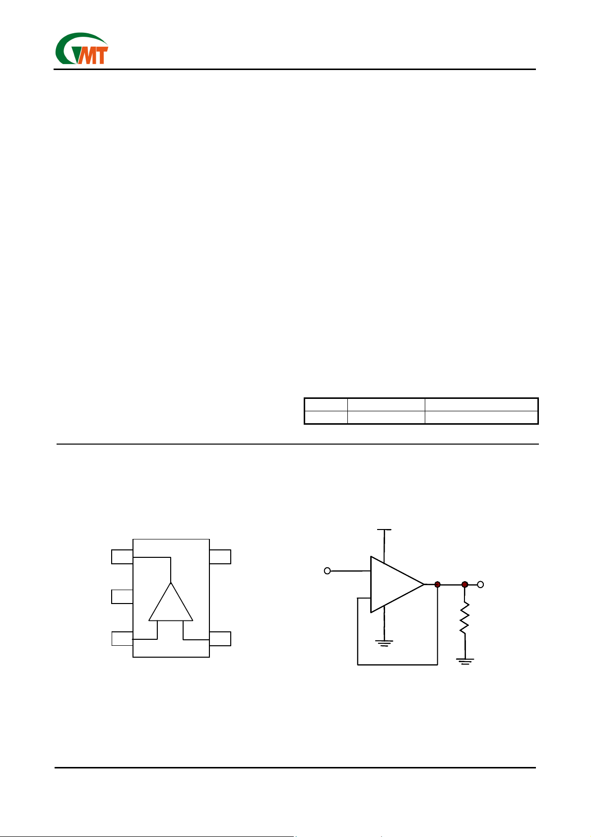
Pin Configuration Typical Application Circuit
VDD
VDD
OUT
OUT
V
V
DD
DD
IN+
IN+
G1212
G1212
V
1
1
2
2
+-
+-
3
3
SOT23-5
SOT23-5
V
5
5
SS
SS
IN
IN
IN
IN-
IN-
4
4
3
3
3
4
4
4
VDD
2
2
2
+
+
+
+
+
+
G121
G1212
G121
G1212
G121
G1212
-
-
-
-
-
-
5
5
5
1
1
1
RL
RL
RL
2K
2K
2K
OUT
OUT
OUT
Ver 1.0
Jul 30, 2001
1
TEL: 886-3-5788833
http://www.gmt.com.tw
Global Mixed-mode Technology Inc.
G1212
Absolute Maximum Ratings
(Note1)
SYMBOL PARAMETER CONDITIONS MIN. MAX. UNIT
VDD Supply voltage 0 7.0 V
T
Storage temperature -65 +150 °C
stg
T
Operating ambient temperature 0 +70 °C
amb
Notes:
1. Absolute Maximum Ratings are limits beyond which damage to the device may occur.
Thermal Characteristics
SYMBOL PARAMETER VALUE UNIT
R
Thermal resistance from junction to ambient in free air SOT23-5 240 °C/W
th j-a
Electrical Characteristics
V
= 2V; VSS = 0V ; T
DD
= 25°C; RL >1M
amb
; unless otherwise specified.
ΩΩΩΩ
SYMBOL PARAMETER CONDITIONS MIN. TYP. MAX. UNIT
Supplies
IDD Supply current no load - 0.13 0.4 mA
P
Total power dissipation no load - 0.26 0.8 mW
tot
DC Characteristics
V
Input offset voltage ±1mV ±15 mV
I (OS)
VCM Common mode voltage 0 - 2.0 V
I
B
I
OS
R
IN
A
V
IO Maximum output current V
VO Output Voltage Swing RL = 2kΩ 0.04 - 1.96 V
PSRR Power supply rejection ratio 50 - dB
CMRR Common-Mode Rejection Ratio 55 dB
AC Characteristics
GBWP Gain-Bandwidth Product Open-loop; No Load - 1.0 - MHz
SR Slew-Rate
PM Phase Margin - 60 - deg
Input Bias Current ±0.05 nA
Input Bias Current Offset ±0.05 nA
Input Resistance 1000 - MΩ
Open Loop Gain 95 - dB
= ±VIN x 90% -
OUT
Measured from 20% to 80% of
step
2V
P-P
12 - mA
±
0.3 V/µs
Ver 1.0
Jul 30, 2001
2
TEL: 886-3-5788833
http://www.gmt.com.tw
 Loading...