

Global Mixed-mode Technology Inc.
G1211
Rail-to-Rail I/O, 100mA Output Op Amp
Features
Single-Supply Operation: 4V to 6V
High Output Current: ±100mA
Low Supply Current: 500 µA
Wide Bandwidth: 3 MHz
Slew Rate: 4 V/µs
No Phase Reversal
Unity Gain Stable
Ultra-Small, 5-Pin SC70 Package
Applications
Battery-Powered Instruments
Portable Equipment
Audio Signal Conditioning
High-Side/Low-Side Current Sensors
Multimedia Audio
ASIC Input or Output Amplifier
Headphone Driver
General Description
The G1211 is a rail-to-rail input and output single-supply amplifiers featuring 100mA output drive
current. This high output current makes these amplifiers excellent for driving either resistive or capacitive
loads. AC performance is very good with 3.0MHz
bandwidth; 4.0V/µs slew rate and low distortion. All
are guaranteed to operate from a +4 to +6 volt single
supply.
The very low input bias currents enable the G1211 to
be used for integrators and diode amplification and
other applications requiring low input bias current. The
100mA high output current and supply current is only
850µA per amplifier at 5 volts, allowing low current
applications to control high current loads.
Applications include audio amplification for computers,
sound ports, sound cards and set-top boxes. The
G1211 is very stable and capable of driving heavy
capacitive loads. The ability to swing rail-to-rail at the
inputs and outputs enables designers to buffer CMOS
ADC/DACs, ASICs or other wide output swing devices
in single-supply systems.
Ordering Information
PART TEMP. RANGE PIN-PACKAGE
G1211 0°C to 70°C SC70-5L
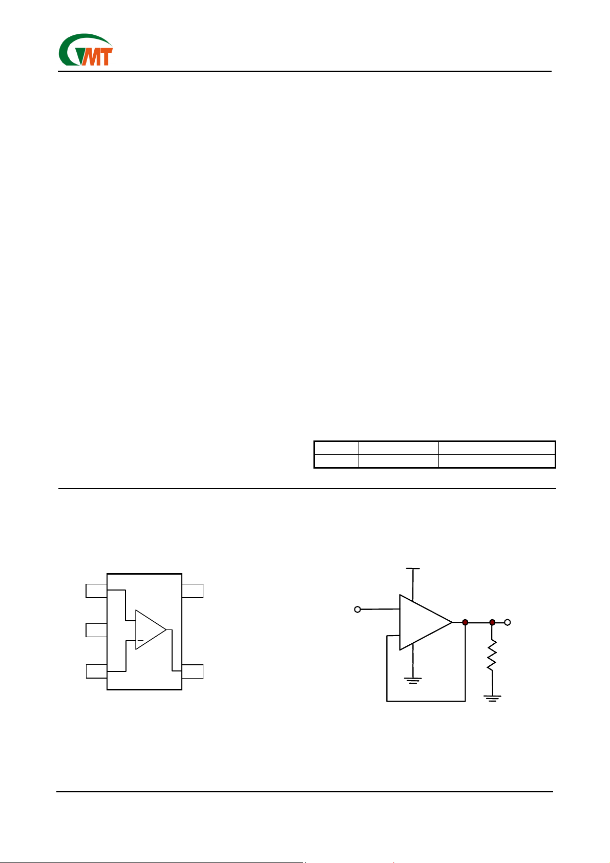
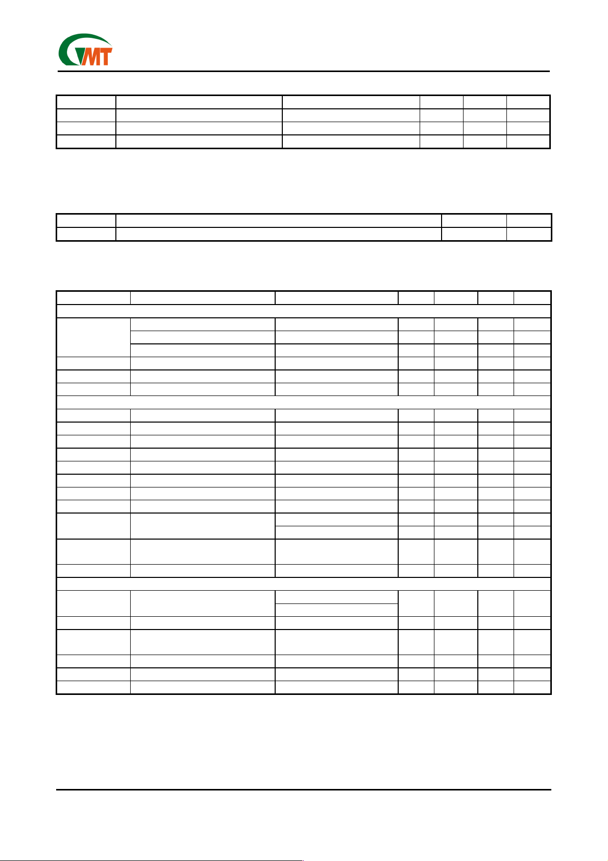
Pin Configuration Tpypical Application Circuit
IN+
IN+
V
V
SS
SS
IN-
IN-
G1211
G1211
V
V
DD
1
1
+
+
2
2
3
3
SC70-5L
SC70-5L
DD
5
5
OUT
OUT
4
4
VDD
VDD
5
5
1
IN
IN
1
3
3
+
+
G1211
G1211
-
-
2
2
4
4
RL
RL
2K
2K
OUT
OUT
Ver 1.3
Oct 23, 2001
1
TEL: 886-3-5788833
http://www.gmt.com.tw
Global Mixed-mode Technology Inc.
G1211
Absolute Maximum Ratings
(Note1)
SYMBOL PARAMETER CONDITIONS MIN. MAX. UNIT
VDD Supply voltage 0 7.0 V
T
Storage temperature -65 +150 °C
stg
T
Operating ambient temperature 0 +70 °C
amb
Notes:
1. Absolute Maximum Ratings are limits beyond which damage to the device may occur.
Thermal Characteristics
SYMBOL PARAMETER VALUE UNIT
R
Thermal resistance from junction to ambient in free air SC70-5L 400 °C/W
th j-a
Electrical Characteristics
V
= 5V; VSS = 0V ; T
DD
= 25°C; fi = 1kHz; RL = 2K
amb
; unless otherwise specified.
ΩΩΩΩ
SYMBOL PARAMETER CONDITIONS MIN. TYP. MAX. UNIT
Supplies
Supply voltage 4.0 5.0 6.0 V
VDD
VSS Negative supply voltage (dual) -2.0 -2.5 -3.0 V
IDD Supply current no load - 0.85 1.2 mA
P
Total power dissipation no load - 4.25 6.0 mW
tot
DC Characteristics
V
I (OS)
VCM Common mode voltage 0 - 5.0 V
I
B
I
OS
R
IN
A
V
IO Maximum output current THD<0.1%, RL= 16Ω - 100 - mA
RO Output resistance Open-loop, RL= 20Ω - 5.5 -
VO Output voltage swing
PSRR Power supply rejection ratio
CMRR Common-Mode Rejection Ratio 56 dB
AC Characteristics
THD Total harmonic distortion
GBWP Gain-Bandwidth Product Open-loop; No Load - 3.0 - MHz
SR Slew-Rate
PM Phase Margin - 60 - deg
PO Maximum output power Note 1; RL = 32Ω - 135 - mW
B Power bandwidth Unity gain; RL = 32Ω - 25 - KHz
Single 4.0 5.0 6.0 V
Dual 2 2.5 3.0 V
Input offset voltage ±1.5 ±10 mV
Input Bias Current ±0.05 nA
Input Bias Current Offset ±0.05 nA
Input Resistance 1000 - MΩ
Large-Signal Voltage Gain 80 - dB
RL = 32Ω 1.0 - 4.0 V
R
= 2kΩ 0.1 - 4.9 V
L
fi = 1kHz;
V
Note 2
R
Measured from 30% to 70% of
5Vp-p step
= 1V
ripple(peak)
= 2kΩ, Note 2
L
Ω
60 - dB
- < 0.1 - %
4 V/µs
Notes:
1. Values are proportional to V
2. V
= 5.0V; V
DD
= 4.0V (at 0 dB)
O (P-P)
Ver 1.3
Oct 23, 2001
; THD < 0.1%
DD
2
TEL: 886-3-5788833
http://www.gmt.com.tw
 Loading...