

Page 1

環天衛星科技股份有限公司
PRODUCT USER MANUAL
GPS ENGINE BOARD
ET-318
Version 1.0
GlobalSat Technology Corporation
台北縣中和市建一路 186 號 16 樓(遠東世紀廣場)
16, No.186,Chien 1 Road, 235Chung Ho City,Taipei Hsien, Taiwan ,R.O.C.
Tel: 886-2-8226-3799(Rep.) Fax: 886-2-8226-3899
Web: www.globalsat.com.tw E-mail: service@globalsat.com.tw
Page 2

Features:
SiRF starⅢ high performance GPS Chip Set
Very high sensitivity (Tracking Sensitivity: -159 dBm)
Extremely fast TTFF (Time To First Fix) at low signal level
Compact size (15.2mm * 14 mm * 2.8mm) suitable for space-sensitive application
One size component, easy to mount on another PCB board
Support NMEA 0183 and SiRF binary protocol
Specification:
General
Chipset SiRF StarⅢ
Frequency L1, 1575.42 MHz
C/A code 1.023 MHz chip rate
Channels 20 channel all-in-view tracking
Sensitivity -159 dBm
Accuracy
Position 10 meters, 2D RMS
5 meters, 2D RMS, WAAS enabled
Velocity 0.1 m/s
Time 1us synchronized to GPS time
Datum
Default WGS-84
Acquisition Time
Reacquisition 0.1 sec., average
Hot start 1 sec., average
Warm start 38 sec., average
Cold start 42 sec., average
Dynamic Conditions
Altitude 18,000 meters (60,000 feet) max
Velocity 515 meters /second (1000 knots) max
Acceleration Less than 4g
Jerk 20m/sec **3
Page 3

Power
Main power input 3.3V +- 5% DC input
Power consumption 42mA (Continuous mode)
36mA (Trickle power mode
Interface
Dimension 15.2mm * 14 mm * 2.8mm
Baud rate 4,800 to 57,600 bps adjustable
Output message SiRF binary or
NMEA 0183 GGA, GSA, GSV, RMC, VTG, GLL
GPS Passive (or Active )Antenna Specification(Recommendation)
Frequency: 1575.42+2 MHz
Axial Ratio: 3 dB Typical
output Impedance: 50Ω
Polarization: RHCP
Output VSWR: 1.5 Max.
Active option
Low Noise Amplifter:
Amplifier Gain :20~26dB Typical
Output VSWR: 2.0 Max.
Noise Figure: 2.0 dB Max.
Environmental
Operating Temperature -40℃ to +85℃
Storage Temperature: -40℃ to +85℃
Page 4
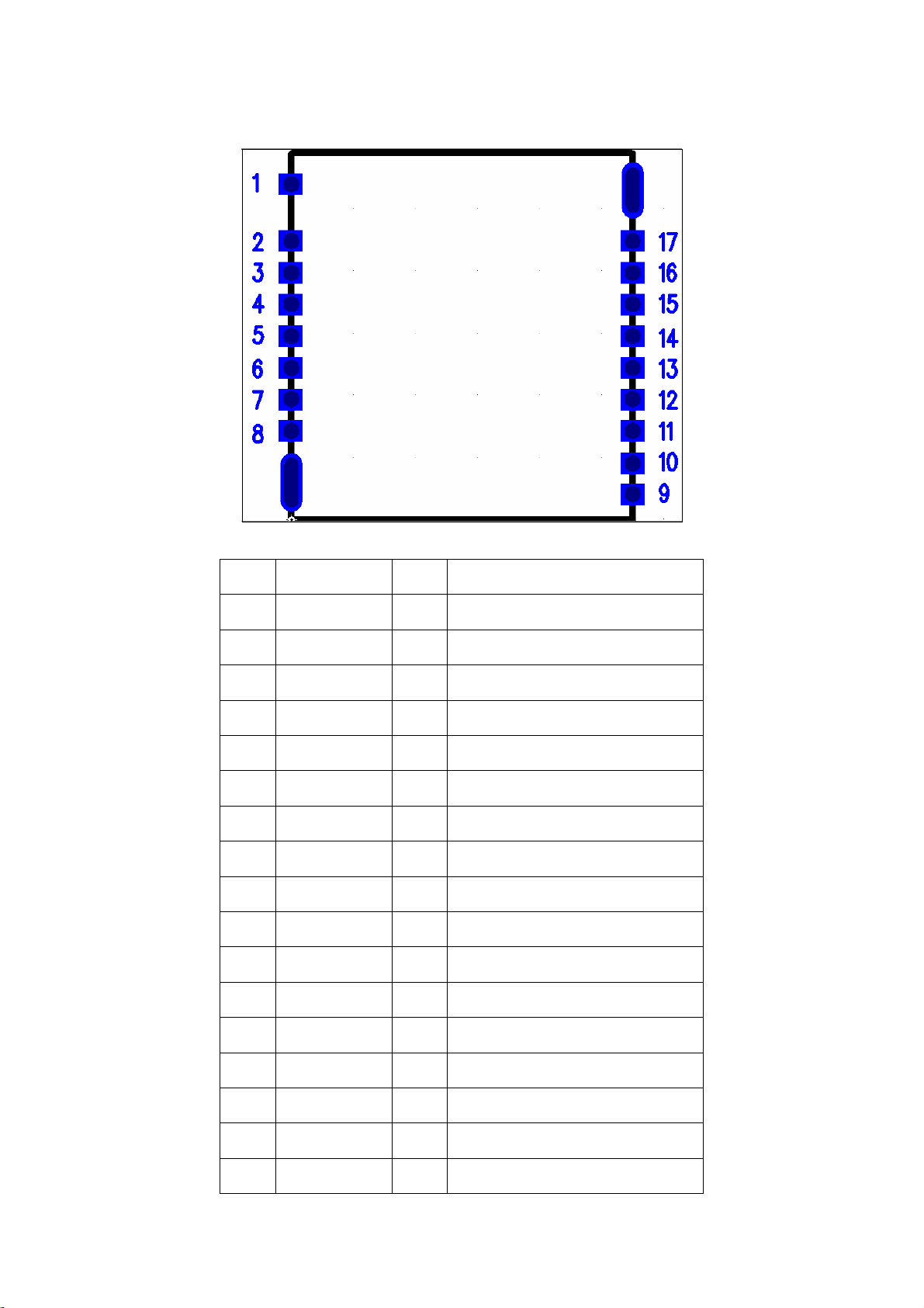
Pin Assignment
Pin Signal Name I/O Description
1 GND G Analog Ground
2 RF_IN RF GPS Signal input
3 GND G Analog Ground
4 NRESET I Reset (Active low)
5 VCC_IN PWR DC Supply Voltage input
6 VBAT PWR Backup voltage supply
7 RXB I Serial port B
8 TXB O Serial port B
9 GND G Analog Ground
10 BOOTSEL Boot mode
11 TXA O Serial port A
12 RXA I Serial port A
13 GPIO1 I General –purpose I/O
14 GPIO14 I General –purpose I/O
15 TIMEMARK O One pulse per second
16 GPIO13 I General –purpose I/O
17 GPIO15 I General –purpose I/O
Page 5

Definition of Pin assignment
VCC_IN
This is the main DC supply for a 3.3V +- 5% DC input power module board.
GND
GND provides the ground for digital pa
BOOTSEL
rt.
Set this pin to high for programming flash.
RXA
This is the main receiver channel and is used to receive software commands to
the
board from SIRFdemo software or from user written software.
PS:
RXB
Pull up
if
not used.
This is the auxiliary receiving channel and is used to input differential
corrections
Pull up
PS:
TXA
This is the main transmitting channel and is used to output
navigation and measurement data to SiRFdemo or user written software.
TXB
to
the board to enable DGPS navigation.
if
not used.
For user’s application (not currently used).
RF_IN
This pin receiver signal of GPS analog .due to the RF characteristics of the
signal
the design has to certain criteria. The line on the PCB from the
antenna(or
PPS
This pin provides one pulse-per-second output from the board,
which is synchronized to GPS time. This is not available in Trickle Power
antenna connector) has to be a controlled microstrip line at 50Ω
mode
.
Page 6
Backup battery (V_BAT)
This is the battery backup input that powers the SRAM and RTC when main
power is removed. Typical current draw is 15uA. Without an external backup
battery, the module/engine board will execute a cold star after every turn on.
To achieve the faster start-up offered by a hot or warm start, a battery backup
must be connected. The battery voltage should be between 2.0v and 5.0v.
TIMEMARK
This pin provides one pulse-per-second output from the
board, which is synchronized to GPS time. This is not available in Trickle
Power mode
GPIO
Functions
Several I/Os are connected to the digital interface connector
for custom applications
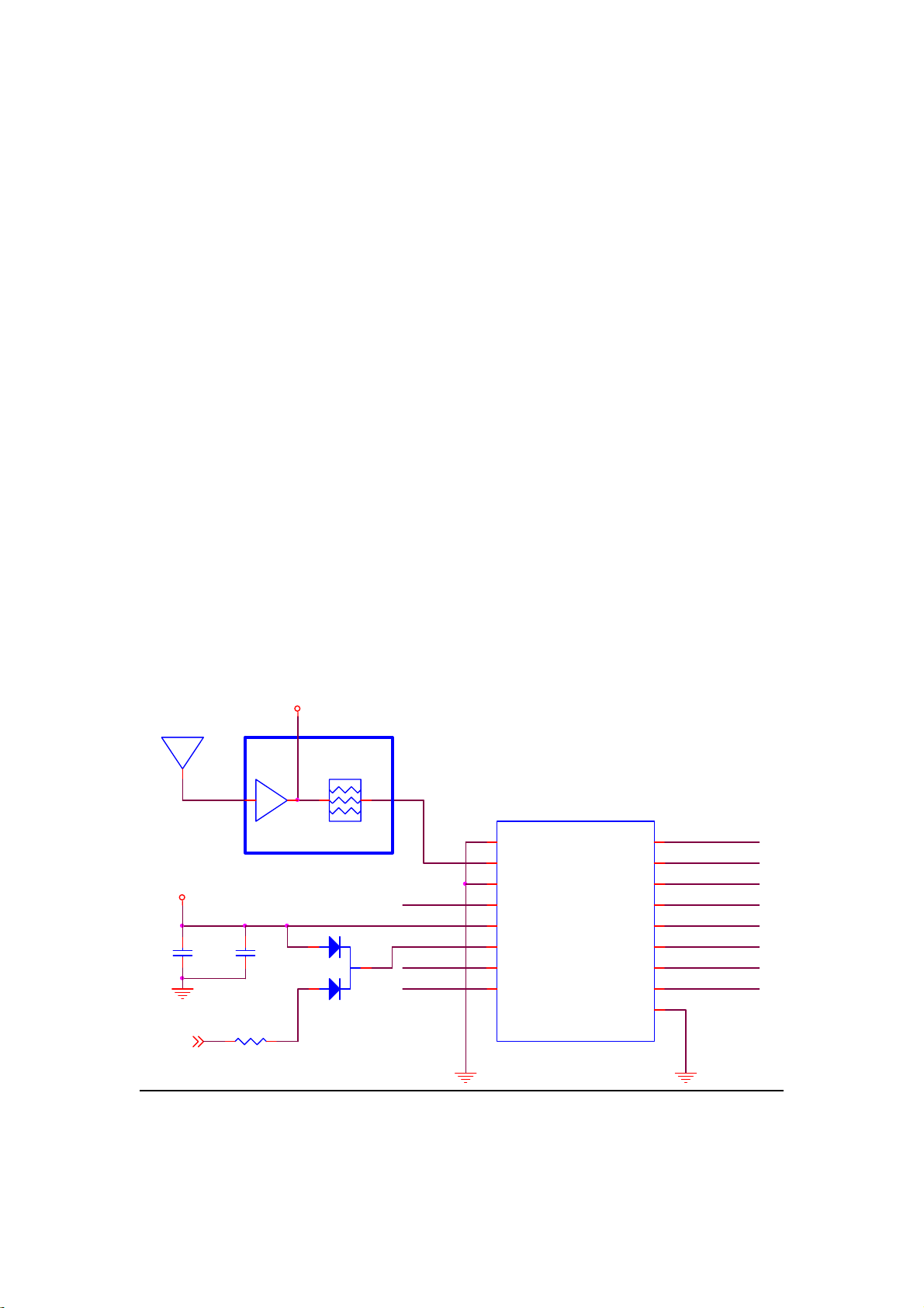
Application Circuit
Antenna
.
1
..
LNA
3.3V
BATTERY
C1
1U
1 2
C2
0.1U
1 2
R46
1 2
560R
.
VCC_RF
R5
1 2
21
SAW FI LTER
option
1
3
RB715F
.
50 ohm m icros trip line
2
RESET
RXB
TXB
1
2
3
4
5
6
7
8
U1
GND
RF_IN
GND
NRESET
VCC_I N
VBAT
RXB
TXB
GPS
GPIO15
GPIO13
TI MEMARK
GPIO14
GPIO1
RXA
TXA
BOOTSEL
GND
17
16
15
14
13
12
11
10
9
GPIO15
GPIO13
TI MEMARK
GPIO14
GPIO1
RXA
TXA
BOOTSEL
Page 7

Recommend Layout PAD
Mechanical Layout
Page 8

r
N
N N
m
t
N
p
d
d
d
d
SOFTWARE COMMAND
NMEA Output Command
GGA-Global Positioning System Fixed Data
Table B-2 contains the values for the following example:
$GPGGA,161229.487,3723.2475,N,12158.3416,W,1,07,1.0,9.0,M,,,,0000*18
Table B-2 GGA Data Format
Name Example Units Description
Message ID $GPGGA GGA protocol heade
UTC Time 161229.487 hhmmss.sss
Latitude 3723.2475 ddmm.mmmm
/S Indicator
Longitude 12158.3416 dddmm.mmm
E/W Indicator W E=east or W=wes
Position Fix Indicator 1 See Table B-3
Satellites Used 07 Range 0 to 12
HDOP 1.0 Horizontal Dilution of Precision
MSL Altitude1 9.0 meters
Units M meters
Geoid Separation
1
meters
Units M meters
Age of Diff. Corr. second
Diff. Ref. Station ID 0000
Checksum *18
<CR><LF> End of message termination
SiRF Technology Inc. does not support geoid corrections. Values are WGS84 ellipsoid heights.
=north or S=south
ull fields when DGPS is not used
Table B-3 Position Fix Indicator
Valu e Descri
0 Fix not available or invali
1 GPS SPS Mode, fix vali
2 Differential GPS, SPS Mode , fix vali
3 GPS PPS Mode, fix vali
tion
Page 9

p
r
N
N
m
t
GLL-Geographic Position-Latitude/Longitude
Table B-4 contains the values for the following example:
$GPGLL,3723.2475,N,12158.3416,W,161229.487,A*2C
Table B-4 GLL Data Format
Name Exam
Message ID $GPGLL GLL protocol heade
Latitude 3723.2475 ddmm.mmmm
/S Indicator n
Longitude 12158.3416 dddmm.mmm
E/W Indicator W E=east or W=wes
UTC Position 161229.487 hhmmss.sss
Status A A=data valid or V=data not valid
Checksum *2C
<CR><LF> End of message termination
le Units Description
=north or S=south
GSA-GNSS DOP and Active Satellites
Table B-5 contains the values for the following example:
$GPGSA,A,3,07,02,26,27,09,04,15,,,,,,1.8,1.0,1.5*33
Table B-5 GSA Data Format
Name Example Units Description
Message ID $GPGSA GSA pr ot ocol header
Mode1 A See Table B-6
Mode2 3 See Table B-7
Satellite Used1 07 Sv on Channel 1
Satellite Used1 02 Sv on Channel 2
…..
Satellite Used1 Sv on Channel 12
PDOP 1.8 Position dilution of Precision
HDOP 1.0 Horizontal dilution of Precision
VDOP 1.5 Vertical dilution of Precision
Checksum *33
<CR><LF> End of message termination
1. Satellite used in solution.
Table B-6 Mode1
Value Description
M Manual-forced to operate in 2D or 3D mode
A 2Dautomatic-allowed to automatically switch 2D/3D
Table B-7 Mode 2
Value Description
1 Fix Not Available
2 2D
3 3D
Page 10

GSV-GNSS Satellites in View
n
r
N
r
)
)
)
)
N
N N
m
t
yy
t
Table B-8 contains the values for the following example:
$GPGSV,2,1,07,07,79,048,42,02,51,062,43,26,36,256,42,27,27,138,42*71
$GPGSV,2,2,07,09,23,313,42,04,19,159,41,15,12,041,42*41
Table B-8 GSV Data Format
Name Example Descriptio
Message ID $GPGSV GSV protocol heade
umber of Messages1 2 Range 1 to 3
Message Numbe
Satellites in View 07
Satellite ID 07 Channel 1(Range 1 to 32
Elevation 79 degrees Channel 1(Maximum90
Azimuth 048 degrees Channel 1(True, Range 0 to 359)
SNR(C/No) 42 dBHz Range 0 to 99,null when not tracking
……. …….
Satellite ID 27 Channel 4 (Range 1 to 32
Elevation 27 Degrees Channel 4(Maximum90
Azimuth 138 Degrees Channel 4(True, Range 0 to 359)
SNR(C/No) 42 dBHz Range 0 to 99,null when not tracking
Checksum *71
<CR><LF> End of message termination
Depending on the number of satellites tracked multiple messages of GSV data may be required.
1
1 Range 1 to 3
RMC-Recommended Minimum Specific GNSS Data
Table B-10 contains the values for the following example:
$GPRMC,161229.487,A,3723.2475,N,12158.3416,W,0.13,309.62,120598,,*10
Table B-10 RMC Data Format
Name Example Units Description
Message ID $GPRMC RMC protocol header
UTC Time 161229.487 hhmmss.sss
Status A A=data valid or V=data not valid
Latitude 3723.2475 ddmm.mmmm
/S Indicator
Longitude 12158.3416 dddmm.mmm
E/W Indicator W E=east or W=wes
Speed Over Ground 0.13 knots
Course Over Ground 309.62 degrees True
Date 120598 ddmm
Magnetic Variation2 degrees E=east or W=wes
Checksum *10
<CR><LF> End of message termination
SiRF Technology Inc. does not support magnetic declination. All “course over ground” data are
=north or S=south
geodetic WGS48 directions.
Page 11

g
g
N
r
VTG-Course Over Ground and Ground Speed
$GPVTG,309.62,T,,M,0.13,N,0.2,K*6E
Name Example Units Description
Message ID $GPVTG VTG protocol header
Course 309.62 degrees Measured headin
Reference T True
Course degrees Measured headin
Reference M Magnetic
Speed 0.13 knots Measured horizontal speed
Units
Speed 0.2 Km/h
Units K Kilometers per hour
Checksum *6E
<CR><LF> End of message termination
Knots
Measured horizontal speed
2.2 NMEA Input Command
A). Set Serial Port ID:100 Set PORTA parameters and protocol
This command message is used to set the protocol(SiRF Binary, NMEA, or
USER1) and/or the communication parameters(baud, data bits, stop bits, parity).
Generally,this command would be used to switch the module back to SiRF Binary
protocol mode where a more extensive command message set is available. For
example,to change navigation parameters. When a valid message is received,the
parameters will be stored in battery backed SRAM and then the receiver will restart
using the saved parameters.
Format:
$PSRF100,<protocol>,<baud>,<DataBits>,<StopBits>,<Parity>*CKSUM
<CR><LF>
<protocol> 0=SiRF Binary, 1=NMEA, 4=USER1
<baud> 1200, 2400, 4800, 9600, 19200, 38400
<DataBits> 8,7. Note that SiRF protocol is only valid f8
Page 12

Data bits
<StopBits> 0,1
<Parity> 0=None, 1=Odd, 2=Even
Example 1: Switch to SiRF Binary protocol at 9600,8,N,1
$PSRF100,0,9600,8,1,0*0C<CR><LF>
Example 2: Switch to User1 protocol at 38400,8,N,1
$PSRF100,4,38400,8,1,0*38<CR><LF>
**Checksum Field: The absolute value calculated by exclusive-OR the
8 data bits of each character in the Sentence,between, but
excluding “$” and “*”. The hexadecimal value of the most
significant and least significant 4 bits of the result are convertted
to two ASCII characters (0-9,A-F) for transmission. The most
significant character is transmitted first.
**<CR><LF> : Hex 0D 0A
B). Navigation lnitialization ID:101 Parameters required for
start
This command is used to initialize the module for a warm start, by providing current
position (in X, Y, Z coordinates),clock offset, and time. This enables the receiver
to search for the correct satellite signals at the correct signal parameters. Correct
initialization parameters will enable the receiver to acquire signals m o re quickly, and
thus, produce a faster navigational solution.
When a valid Navigation Initialization command is received, the receiver will restart
using the input parameters as a basis for satellite selection and acquisition.
Format:
$PSRF101,<X>,<Y>,<Z>,<ClkOffset>,<TimeOfWeek>,<WeekNo>,<chnlCount>,<R
esetCfg>
*CKSUM<CR><LF>
<X> X coordinate position
INT32
Page 13

<Y> Y coordinate position
INT32
<Z> Z coordinate position
INT32
<ClkOffset> Clock offset of the receiver in Hz, Use 0 for
last saved value if available. If this is
unavailable, a default value of 75000 for
GSP1, 95000 for GSP 1/LX will be used.
INT32
<TimeOf Week> GPS Time Of Week
UINT32
<WeekNo> GPS Week Number
UINT16
( Week No and Time Of Week calculation
from UTC time)
<chnlCount> Number of channels to use.1-12. If your
CPU throughput is not high enough, you
could decrease needed throughput by
reducing the number of active channels
UBYTE
<ResetCfg> bit mask
0×01=Data Valid warm/hotstarts=1
0×02=clear ephemeris warm start=1
0×04=clear memory. Cold start=1
UBYTE
Example: Start using known position and time.
$PSRF101,-2686700,-4304200,3851624,96000,497260,921,12,3*7F
C). Set DGPS Port ID:102 Set PORT B parameters for DGPS input
This command is used to control Serial Port B that is an input only serial port
used to receive
RTCM differential corrections.
Differential receivers may output corrections using different
communication parameters.
Page 14

The default communication parameters for PORT B are 9600
Baud, 8data bits, 0 stop bits, and no parity.
If a DGPS receiver is used which has different communication parameters, use
this command to allow the receiver to correctly decode the data. When a valid
message is received, the parameters will be stored in battery backed SRAM and
then the receiver will restart using the saved parameters.
Format:
$PSRF102,<Baud>,<DataBits>,<StopBits>,<Parity>*CKSUM<CR><LF>
<baud> 1200,2400,4800,9600,19200,38400
<DataBits> 8
<StopBits> 0,1
<Parity> 0=None,Odd=1,Even=2
Example: Set DGPS Port to be 9600,8,N,1
$PSRF102,9600,8,1.0*12
D). Query/Rate Control ID:103 Query standard NMEA message and/or set
output rate
This command is used to control the output of standard NMEA message GGA,
GLL, GSA, GSV
RMC, VTG. Using this command message, standard NMEA message may be
polled once, or setup for periodic output. Checksums may also be enabled
or disabled depending on the needs of the receiving program. NMEA
message settings are saved in battery backed memory for each entry when the
message is accepted.
Format:
$PSRF103,<msg>,<mode>,<rate>,<cksumEnable>*CKSUM<CR><LF>
<msg>
0=GGA,1=GLL,2=GSA,3=GSV,4=RMC,5=VTG
<mode> 0=SetRate,1=Query
<rate> Output every <rate>seconds, off=0,max=255
<cksumEnable> 0=disable Checksum,1=Enable checksum
for specified message
Page 15

Example 1: Query the GGA message with checksum enabled
$PSRF103,00,01,00,01*25
Example 2: Enable VTG message for a 1Hz constant output with checksum
enabled
$PSRF103,05,00,01,01*20
Example 3: Disable VTG message
$PSRF103,05,00,00,01*21
E). LLA Navigation lnitialization ID:104 Parameters required to start
using Lat/Lon/Alt
This command is used to initialize the module for a warm start, by providing
current position (in Latitude, Longitude, Altitude coordinates), clock offset, and
time. This enables the receiver to search for the correct satellite signals at
the correct signal parameters. Correct initialization parameters will enable
the receiver to acquire signals more quickly, and thus, will produce a faster
navigational soution.
When a valid LLANavigationInitialization command is received,the receiver will
restart using the input parameters as a basis for satellite selection and acquisition.
Format:
$PSRF104,<Lat>,<Lon>,<Alt>,<ClkOffset>,<TimeOfWeek>,<WeekNo>,
<ChannelCount>, <ResetCfg>*CKSUM<CR><LF>
<Lat> Latitude position, assumed positive north of equator and
negative south of equator float, possibly signed
<Lon> Longitude position, it is assumed positive east of Greenwich
Page 16

and negative west of Greenwich
Float, possibly signed
<Alt> Altitude position
float, possibly signed
<ClkOffset> Clock Offset of the receiver in Hz, use 0 for last saved value if
available. If this is unavailable, a default value of 75000 for
GSP1, 95000 for GSP1/LX will be used.
INT32
<TimeOfWeek> GPS Time Of Week
UINT32
<WeekNo> GPS Week Number
UINT16
<ChannelCount> Number of channels to use. 1-12
UBYTE
<ResetCfg> bit mask 0×01=Data Valid warm/hot starts=1
0×02=clear ephemeris warm start=1
0×04=clear memory. Cold start=1
UBYTE
Example: Start using known position and tim e.
$PSRF104,37.3875111,-121.97232,0,96000,237759,922,12,3*37
F). Development Data On/Off ID:105 Switch Development Data
Messages On/Off
Use this command to enable development debug information if you are having
trouble getting commands accepted. Invalid commands will generate debug
information that should enable the user to determine the source of the
command rejection. Common reasons for input command rejection are invalid
checksum or parameter out of specified range. This setting is not preserved
across a module reset.
Format: $PSRF105,<debug>*CKSUM<CR><LF>
<debug> 0=Off,1=On
Page 17

Example: Debug On $PSRF105,1*3E
Example: Debug Off $PSRF105,0*3F
G). Select Datum ID:106 Selection of datum to be used for coordinate
Transformations
GPS receivers perform initial position and velocity calculations using an
earth-centered earth-fixed (ECEF) coordinate system. Results may be converted
to an earth model (geoid) defined by the selected datum. The default datum is
WGS 84 (World Geodetic System 1984) which provides a worldwide common
grid system that may be translated into local coordinate systems or map datums.
(Local map datums are a best fit to the local shape of the earth and not valid
worldwide.)
Examples:
Datum select TOKYO_MEAN
$PSRF106,178*32
 Loading...