Global Mixed-mode Technology G913 Technology Manual

查询G913供应商
Global Mixed-mode Technology Inc.
150mA Low-Dropout Linear Regulators
Features
Low, 55µA No-Load Supply Current
Guaranteed 150mA Output Current
Dropout Voltage is 70mV @ 50mA Load
Over-Temperature Protection and Short-Circuit
Protection
Two Modes of Operation ----
Fixed Mode: 2.84V (G913A), 3.15V (G913B),
3.30V (G913C), 3.00V (G913D)
Adjustable Mode: from 1.25V to 5.5V
Max. Supply Current in Shutdown Mode < 1µA
Low Output Noise at 220µV
Stability with lost cost ceramic capacitors
Applications
Notebook Computers
Cellular Phones
PDAs
Digital still Camera and Video Recorders
Hand-Held Devices
Bar Code Scanners
RMS
G913
General Description
The G913 is a low supply current, low dropout linear
regulator that comes in a space saving SOT23-5 package. The supply current at no-load is 55µA. In the
shutdown mode, the maximum supply current is less
than 1µA. Operating voltage range of the G913 is from
2.5V to 5.5V. The over-current protection limit is set at
250mA typical and 150mA minimum. An overtemperature protection circuit is built-in in the G913 to
prevent thermal overload. These power saving features make the G913 ideal for use in the battery-powered applications such as notebook computers, cellular phones, and PDA’s.
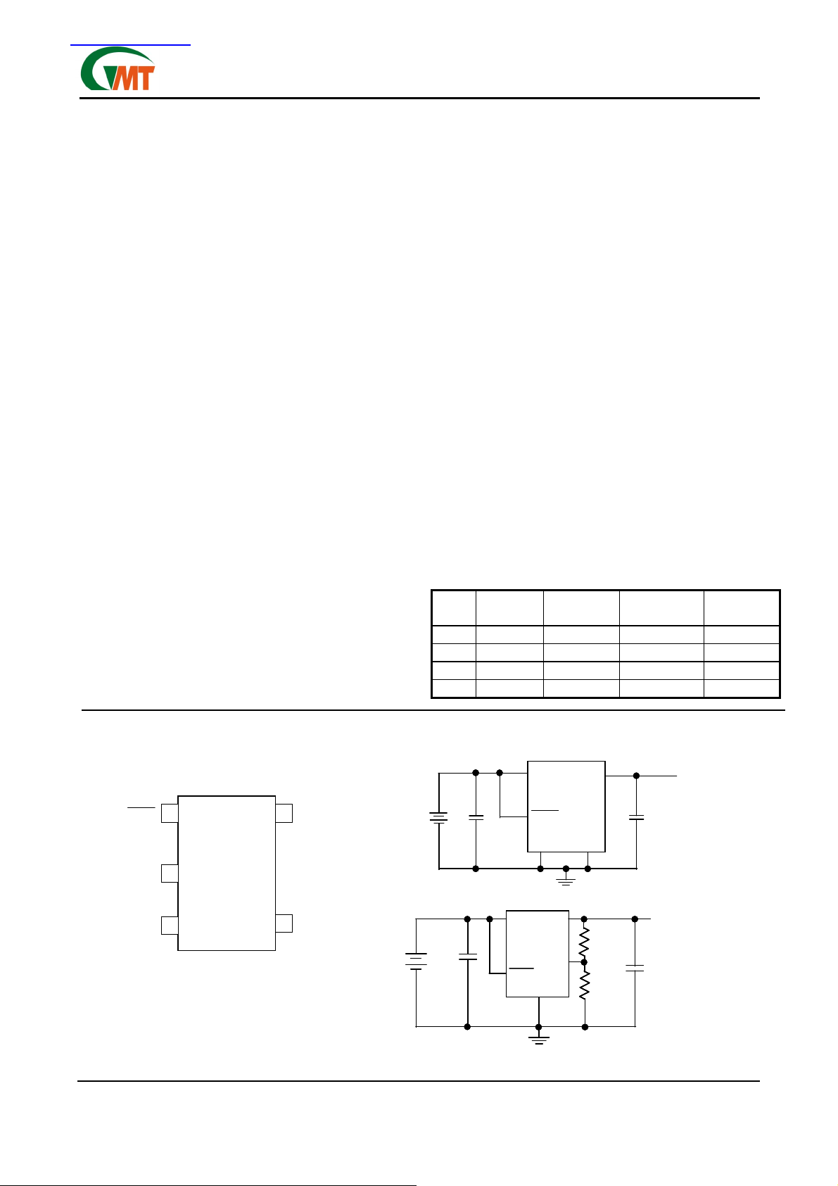
The G913 has two modes of operation. When the SET
pin is connected to ground, its output is a pre-set
value: 2.84V for G913A, 3.15V for G913B, and 3.30V
for G913C, and 3.00V for G913D. There is no external
components needed to decide the output voltage.
When an output other than the preset value is needed,
two external resistors should be used as a voltage
divider. The output voltage is then decided by the resistor ratio. The G913 comes in a space saving
SOT23-5 package.
Pin Configuration
1
1
1
SHDN
SHDN
SHDN
2
2
2
GND
GND
GND
IN
IN
IN
3
3
3
G963
G963
G963
G913
G913
G913
SOT23-5
SOT23-5
SOT23-5
Ordering Information
PART MARKING VOLTAGE
TEMP.
RANGE
G913A 3A 2.84 -40°C~ +85°C SOT 23-5
G913B 3B 3.15 -40°C~ +85°C SOT 23-5
G913C 3C 3.30 -40°C~ +85°C SOT 23-5
G913D 3D 3.00 -40°C~ +85°C SOT 23-5
OUTPUT
OUTPUT
C
C
C
OUT
OUT
OUT
1µF
1µF
1µF
OUTPUT
OUTPUT
OUTPUT
VOLTAGE
VOLTAGE
VOLTAGE
C
C
C
OUT
OUT
OUT
1µF
1µF
1µF
OUTPUT
VOLTAGE
VOLTAGE
VOLTAGE
IN OUT
IN OUT
IN OUT
G913
G913
+
+
+
C
C
C
IN
IN
5
5
5
SET
SET
SET
BATTERY
BATTERY
BATTERY
4
4
4
OUT
OUT
OUT
+
+
+
-
-
-
1µF
1µF
1µF
_
_
_
BATTERY
BATTERY
BATTERY
IN
IN
IN
IN
C
C
C
SHDN
SHDN
SHDN
IN
IN
IN
1µF
1µF
1µF
G913
SHDN
SHDN
SHDN
GND
GND
GND
Fixed mode
Fixed mode
Fixed mode
OUT
OUT
OUT
G913
G913
G913
SET
SET
SET
GND
GND
GND
SET
SET
SET
R1
R1
R1
R2
R2
R2
PIN-
PACKAGE
Ver 0.9 Preliminary
Jan 25, 2002
1
Adjustable mode
Adjustable mode
Adjustable mode
TEL: 886-3-5788833
http://www.gmt.com.tw

Absolute Maximum Ratings
VIN to GND……………………………………-0.3V to +7V
Output Short-Circuit Duration………………….….Infinite
SET to GND.……………………………..…..-0.3V to +7V
SHDN to GND…………………..………….-0.3V to +7V
SHDNto IN….…………………..…………..-7V to +0.3V
OUT to GND…………………………-0.3V to (V
Note (1): See Recommended Minimum Footprint (Figure 3)
Stresses beyond those li sted under "Absolute Maximum Ratings" may cause permanent damage to the device. These are stres s ratings only, and functional operat i on of the device at these or any other condit i ons beyond those indicated in the operational sections of
the specifications is not implied. Exposure to absolute maximum rating c ondi tions for extended periods may affect devi ce reliability.
Global Mixed-mode Technology Inc.
Continuous Power Dissipation (T
SOT23-5……………………………………...…..520 mW
Operating Temperature Range………...-40°C to +85°C
Junction Temperature……………………….……+150°C
(1)
….…..…………….…………….…..…..240°C/Watt
θ
JA
Storage Temperature Range………….-65°C to +160°C
Lead Temperature (soldering, 10sec)..…………+300°C
+ 0.3V)
IN
= +25°C)
A
G913
Electrical Characteristics
(V
=+3.6V, V
IN
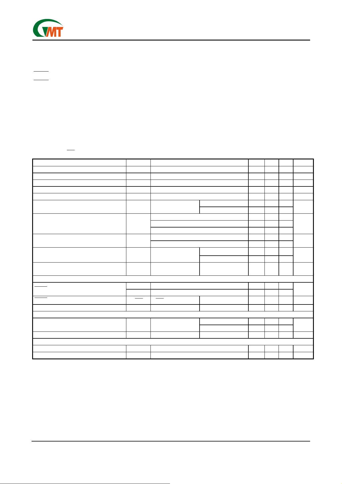
Input Voltage (Note 2) VIN 2.5 5.5 V
Output Voltage Accuracy V
Adjustable Output Voltage Range (Note 3) V
Maximum Output Current 150 mA
Current Limit (Note 4) I
Ground Pin Current IQ SET = GND
Dropout Voltage (Note 5) V
Line Regulation
Load Regulation
Output Voltage Noise (10Hz to 100kHz) en
SHUTDOWN
SHDN
Input Threshold
SHDN
Input Bias Current
Shutdown Supply Current I
SET INPUT
SET Reference Voltage (Not e 3) V
SET Input Leakage Current ( N ote 3) I
THERMAL PROTECTION
Thermal Shutdown Temperature T
Thermal Shutdown Hysteres is
Note 1: Limits is 100% production tested at T
Note 2: Guaranteed by line regulation test.
Note 3: Adjustable mode only.
Note 4: Not tested. For design purposes, the current limit should be considered 150mA minimum to 420mA m axim um.
Note 5: The dropout voltage is defined as (V
SHDN
=VIN, TA =TJ =+25°C, unless otherwise noted.) (Note 1)
PARAMETER SYMBOL CONDITIONS MIN TYP MAX UNITS
Variation from specified V
OUT
V
OUT
250 mA
LIM
I
= 1mA 2
OUT
I
= 50mA 70
OUT
I
=150mA 230 300
OUT
SET=GND, VIN=V
SET tied to OUT , V
I
= 0mA to 150mA
OUT
V
=4.2V,
IN
=150mA
I
OUT
+0.1V,to 5.5V I
(STD)
=2.5V to 5.5V , I
IN
∆
∆
DROP
V
LNR
V
LDR
VIH Regulator enabled VIN-0.7
V
Regulator shutdown 0.4
IL
I
SHDN
QSHDN
V
V
= VIN
SHDN
= 0V TA = +25°C 0.2 1 µA
OUT
V
= 2.5V to 5.5V,
IN
SHDN
T
∆
SET
V
SET
SHDN
= 1mA
I
OUT
= 1.3V TA = +25°C 5 30 nA
SET
150 °C
15 °C
= +25°C. Low duty pulse techniques are used during test to
A
, I
=1mA -2 2 %
OUT
5.5 V
SET
= 0mA 55 120
= 50mA 145
= 1m A 0.1 0.28
OUT
= 1m A 0.08 0.4
OUT
I
LOAD
I
LOAD
OUT
SET tied to OUT 0.02 0.8
SET = GND 1.0
C
= 1µF 220 µV
OUT
T
= +25°C
A
0.003 0.1 µA
TA = +25°C 1.225 1.25 1.275
= T
to T
T
A
MIN
1.25
MAX
µA
mV
%/V
%
RMS
V
V
maintain junction temperature as close to ambient as possible.
IN-VOUT
) when V
is 100mV below the value of V
OUT
for VIN = V
OUT
OUT
+2V,
The performance of every G913 part, see “Typical Performance Characteristics”.
Ver 0.9 Preliminary
Jan 25, 2002
2
TEL: 886-3-5788833
http://www.gmt.com.tw

Global Mixed-mode Technology Inc.
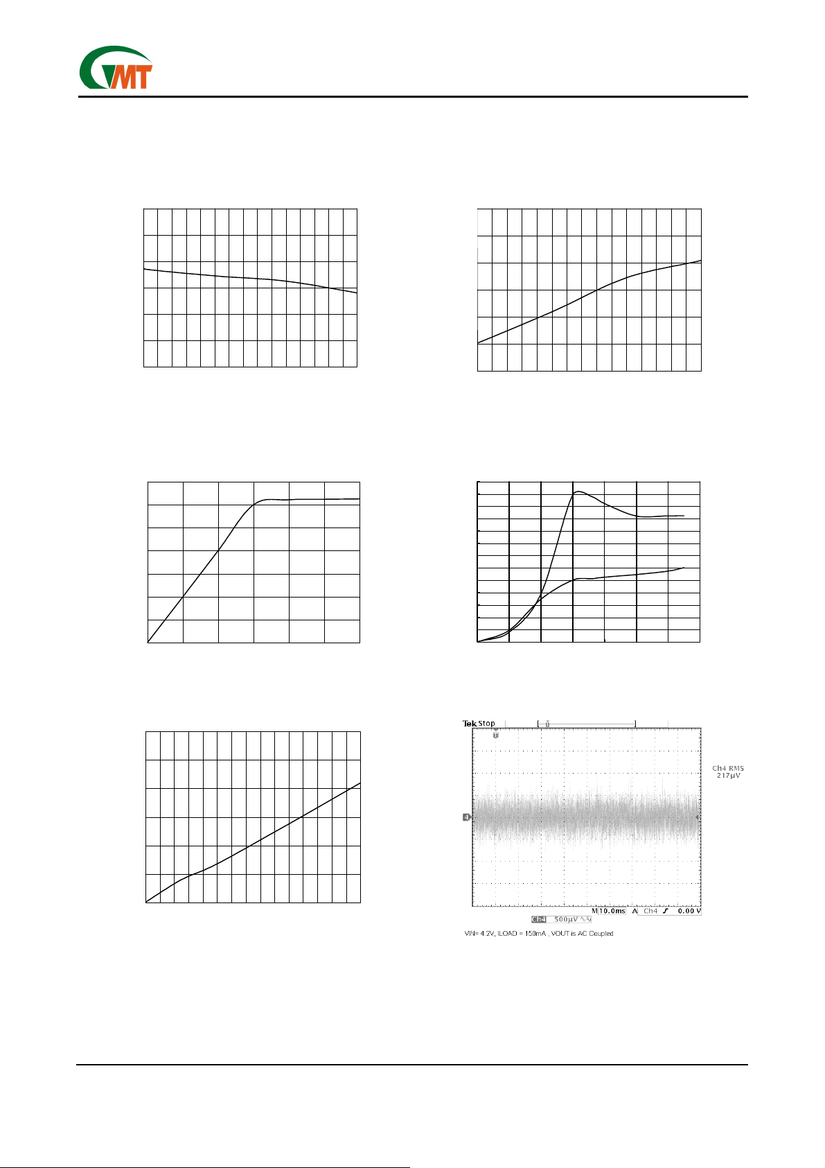
Typical Performance Characteristics
(VIN= +3.6V, CIN=1µF, C
Output Voltage vs. Load Current Ground Current vs. Load Current
=1µF, G913B, TA=25 °C, unless otherwise noted.)
OUT
G913
3.160
3.150
300
250
A)
3.140
3.130
3.120
Output Voltage (V)
3.110
3.100
0 102030405060708090100110120130140150
Load Current (mA)
μ
200
150
100
50
Ground Current (
0
0 102030405060708090100110120130140150
Load Current (mA)
Output Voltage vs. Load C urrent Supp ly Current vs. Input Volt age
3.50
3.00
2.50
2.00
1.50
1.00
Output Voltage (V)
0.50
0.00
0123456
Input Voltage (V)
No Load
130
120
110
100
A)
90
μ
80
70
60
50
40
30
20
Supply Current (
10
0
01234567
Input Voltage (V)
I
LOAD
I
LOAD
= 50mA
= 0A
Dropou t Voltage v s. Load Current Output Noise 10HZ to 100KHZ
300
250
200
150
100
50
Dropout Voltage (mV)
0
0 102030405060708090100110120130140150
Load Current (mA)
Ver 0.9 Preliminary
Jan 25, 2002
3
TEL: 886-3-5788833
http://www.gmt.com.tw
 Loading...