Global Mixed-mode Technology G2995 Technology Manual

查询G2995供应商
Global Mixed-mode Technology Inc.
G2995
DDR Termination Regulator
Features
Operation Supply Voltage: 1.6V to 5.5V
Low Supply Current: 280µA @ 2.5V
Low Output Offset
Source and Sink Current
Low External Component Count
No Inductor Required
No external Resistors Required
Thermal Shutdown Protection
SOP-8L with Power-Pad package
Applications
DDR-SDRAM Termination Voltage
DDR-I / DDR-II Termination Voltage
SSTL-2
SSTL-3
Ordering Information
General Description
The G2995 is a linear regulator designed to meet the
JEDEC SSTL-2 and SSTL-3 (Series Stub Termination
Logic) specifications for termination of DDR-SDRAM.
It contains a high-speed operational amplifier that provides excellent response to the load transients. This
device can deliver 1.5A continuous current and transient peaks up to 3A in the application as required for
DDR-SDRAM termination. With an independent V
pin, the G2995 can provide superior load regulation.
The G2995 provides a V
output as the reference for
REF
the applications of the chipset and DIMMs.
The G2995 can easily provide the accurate V
V
voltages without external resistors that PCB ar-
REF
eas can be reduced. The quiescent current is as low
as 280µA @ 2.5V. So the power consumption can
meet the low power consumption applications.
SENSE
and
TT
ORDER
NUMBER
ORDER NUMBER
(Pb free)
MARKING
TEMP.
RANGE
G2995P1U G2995P1Uf G2995 -40°C to 85°C SOP-8
G2995F1U G2995F1Uf G2995 -40°C to 85°C SOP-8 (FD)
Note: P1:SOP-8 F1:SOP-8(FD)
U: Tape & Reel (FD): Thermal Pad
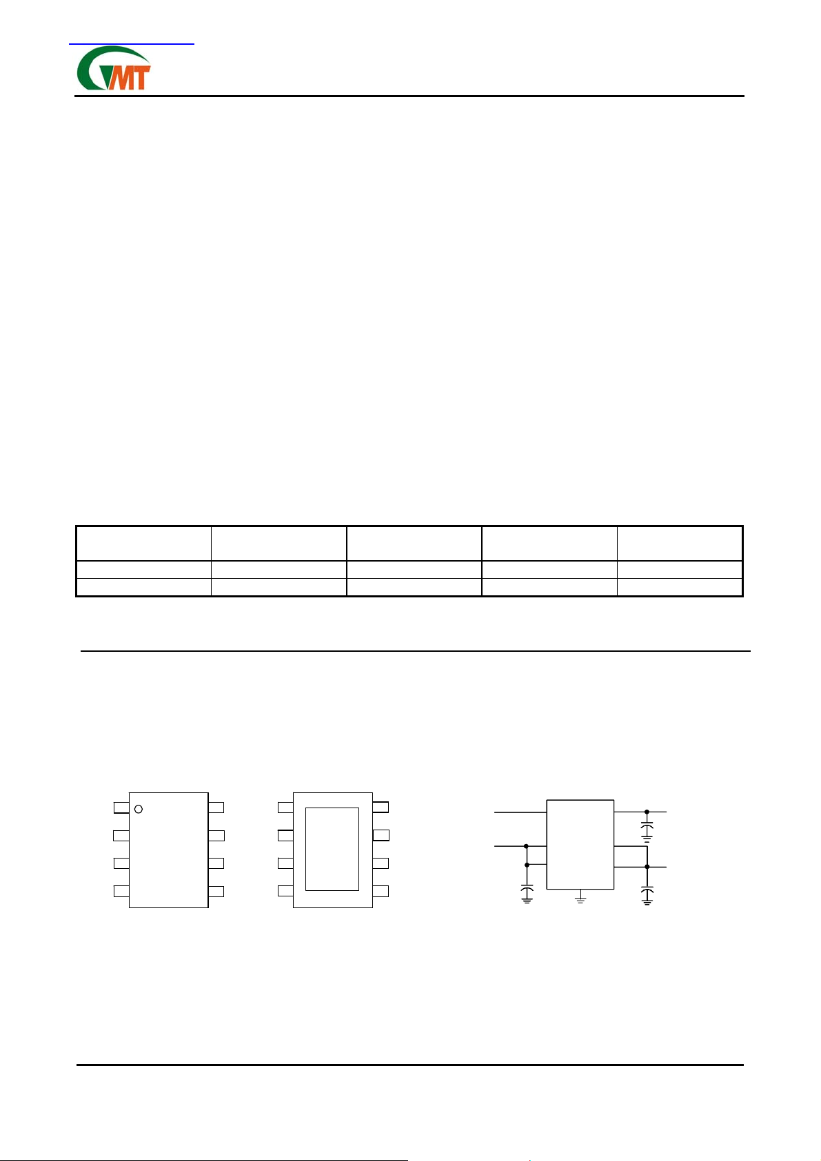
Pin Configuration Typical Application Circuit
NC
NC
GND
GND
VSENSE
VSENSE
VREF
VREF
G2995
G2995
8
1
1
2
2
3
3
4
4
SOP-8
SOP-8
8
VTT
VTT
7
7
PVIN
PVIN
AVIN
AVIN
6
6
VDDQ
VDDQ
5
5
Thermal
Thermal
Pad
Pad
V
=2.5V
=2.5V
V
V
DDQ
DDQ
V
V
=2.5V
=2.5V
DD
DD
47µF
47µF
V
AV
AV
PV
PV
+
+
DDQ
DDQ
V
V
REF
REF
V
V
IN
IN
SENSE
SENSE
V
V
IN
IN
GND
GND
TT
TT
PACKAGE
=1.25V
=1.25V
V
V
REF
REF
+
+
0.01µF
0.01µF
VTT=1.25V
VTT=1.25V
+
+
220µF
220µF
Ver: 1.7
May 10, 2005
1
TEL: 886-3-5788833
http://www.gmt.com.tw

Global Mixed-mode Technology Inc.
Absolute Maximum Ratings
Supply Voltage
PVIN, AVIN, VDDQ to GND……………-0.3V to +6V
Operating Ambient Temperature Range
T
…….…………………………….……...-40°C to +125°C
A
Maximum Junction Temperature, T
Storage Temperature Range, T
STG
(1)
…..……….….150°C
J
….….-65°C to+150°C
Recommend Operation Range
Operating Ambient Temperature Range
T
…….…………………………….……….-40°C to +85°C
A
AVIN to GND………………………..………1.6V to +5.5V
PVIN, VDDQ to GND.………………………1.6V to AVIN
G2995
Reflow Temperature (Soldering, 10 sec)…………260°C
Electrostatic Discharge, V
Human body mode..………………………………2000V
SOP-8L Thermal Resistance (θ
SOP-8L (FD) Thermal Resistance (θ
SOP-8L (FD) Thermal Resistance (θ
SOP-8L (FD) Thermal Resistance (θJc)……….12°C/W
Note:
(1)
:Absolute maximum rating indicates limits beyond which damage to the device may occurs.
(2)
: Human body model : C = 100pF, R = 1500Ω, 3 positive pulses plus 3 negative pulses
(3)
: The package is placed on a 2-layer PCB (2oz/2oz) with 6 vias.
(4)
: The package is placed on a 2-layer PCB (2oz/2oz) with 6 vias. The airflow is used.
ESD
)…….………130°C/W
JA
)……...50°C/W
JA
)………41°C/W
JA
(2)
(3)
(4)
Electrical Characteristics
Specifications with standard typeface are for TA=25°C. Unless otherwise specified, AVIN=PVIN=2.5V, VDDQ=2.5V
PARAMETER SYMBOL CONDITION MIN TYP MAX UNIT
V
Voltage V
REF
V
Output impendence Z
REF
REF
REF
VTT Output voltage VTT
V
VTT Output Voltage Offset (V
REF- VTT
)
Quiescent Current I
VDDQ input Impedence Z
V
input current I
SENSE
os
Q
VDDQ
SENSE
Thermal Shutdown TSD
Thermal Shutdown Hystersis T
Hsy
VDDQ=2.3V
VDDQ=2.5V
VDDQ=2.7V
I
=-30µA to + 30µA --- 1.15 ---
REF
I
=0A
OUT
VDDQ=2.3V
VDDQ=2.5V
VDDQ=2.7V
=±1.5A
I
OUT
VDDQ=2.3V
VDDQ=2.5V
VDDQ=2.7V
I
=0A
OUT
Vtt
=-1.5A
I
OUT
I
=+1.5A
OUT
I
=0A --- 280 500 µA
OUT
--- 100 ---
1.11
1.21
1.31
1.11
1.21
1.31
1.11
1.21
1.31
-40
-40
-40
1.145
1.245
1.345
1.152
1.252
1.352
1.152
1.252
1.352
0
0
0
1.19
1.29
1.39
1.19
1.29
1.39
1.19
1.29
1.39
40
40
40
V
V
V
kΩ
V
V
V
V
V
V
mV
mV
mV
KΩ
--- 20 --- nA
--- 150 ---
--- 25 ---
°C
°C
Ver: 1.7
May 10, 2005
2
TEL: 886-3-5788833
http://www.gmt.com.tw

Global Mixed-mode Technology Inc.
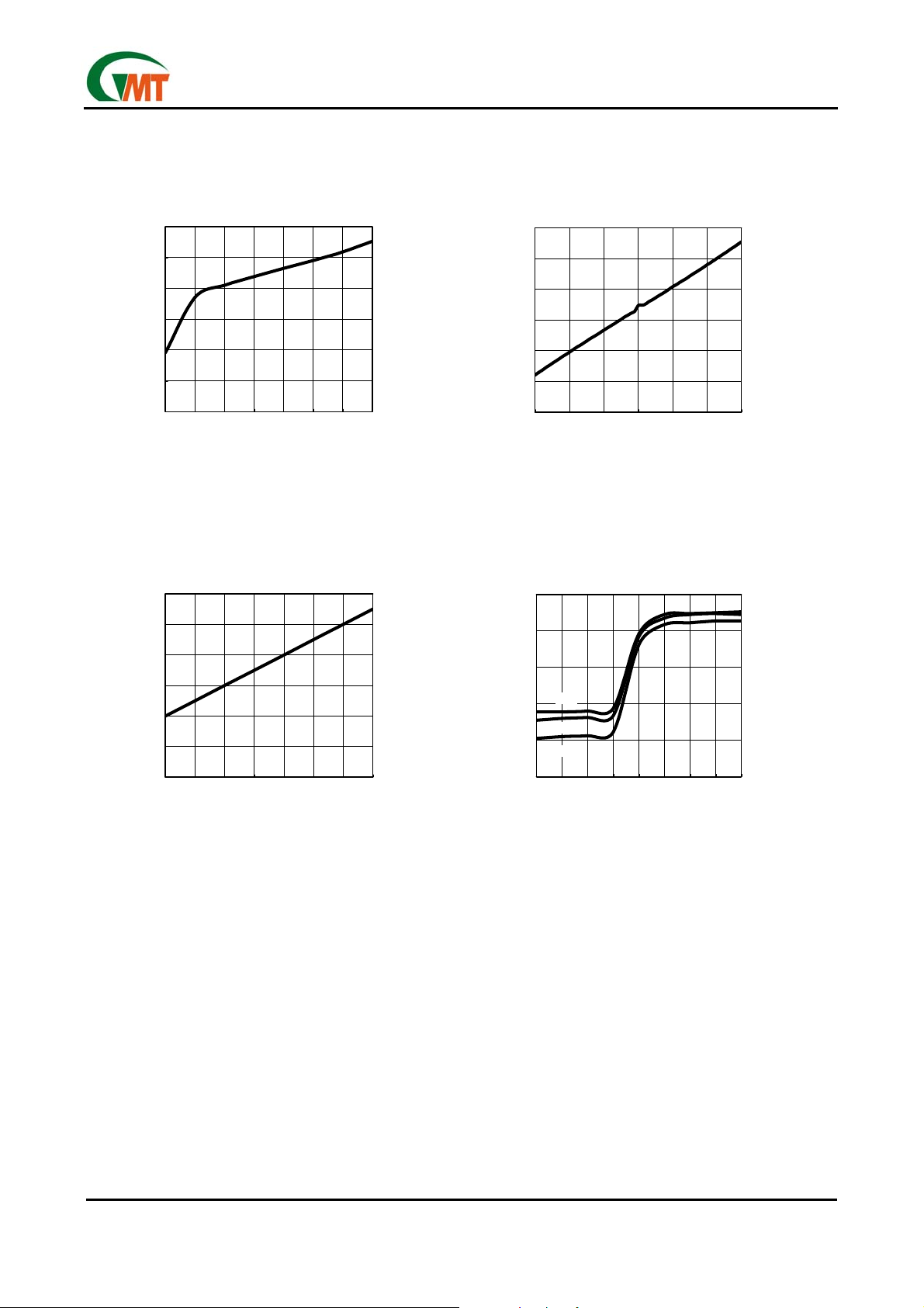
Typical Performance Characteristics
AVIN=2.5V, P
wise noted.
=2.5V, V
VIN
=2.5V, C
DDQ
=0.1µF, C
AVIN
PVIN
=47µF, C
=0.01µF, C
VREF
G2995
=220µF, TA=25°C, unless other-
VTT
270
IQ vs AV
250
230
210
(µA)
Q
I
190
170
150
22.533.544.555.5
V
3
2.5
2
(V)
1.5
REF
V
1
0.5
0
22.533.544.555.5
REF
AVIN(V)
vs V
V
DDQ
IN
DDQ
(V)
V
vs I
REF
1.3
1.28
1.26
(V)
1.24
REF
V
1.22
1.2
1.18
-30 -20 -10 0 10 20 30
VTT vs I
0°C
1.24
25°C
85°C
-100 -75 -50 -25 0 25 50 75 100
(V)
V
1.252
1.248
1.244
TT
1.236
1.232
REF
I
(µA)
REF
Temperature
OUT
I
(mA)
OUT
Ver: 1.7
May 10, 2005
3
TEL: 886-3-5788833
http://www.gmt.com.tw

Global Mixed-mode Technology Inc.
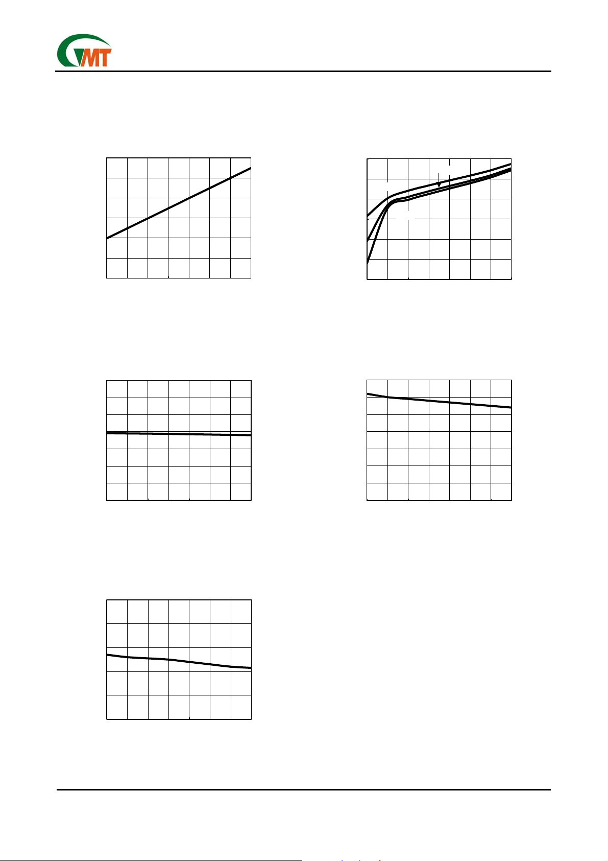
Typical Performance Characteristics
AVIN=2.5V, P
wise noted.
2.5
(V)
1.5
TT
V
3
2
1
=2.5V, V
VIN
=2.5V, C
DDQ
VTT vs V
DDQ
=0.1µF, C
AVIN
PVIN
=47µF, C
=0.01µF, C
VREF
(µA)
Q
I
270
250
230
210
190
G2995
=220µF, TA=25°C, unless other-
VTT
IQ vs AVIN Temperature
25°C
85°C
0°C
0.5
0
22.533.544.555.5
V
(V)
DDQ
Maximum Sourcing Current vs AV
(V
=2.5V, PVIN=1.8V)
DDQ
1.4
1.2
1
0.8
0.6
0.4
OUTPUT CURRENT(A)
0.2
0
22.533.544.555.5
AVIN(V)
170
150
22.533.544.555.5
AVIN(V)
IN
Maximum Sourcing Current vs AV
(V
=2.5V, PVIN=2.5V)
1.8
1.7
1.6
1.5
1.4
1.3
OUTPUT CURRENT(A)
1.2
1.1
22.533.544.555.5
DDQ
AVIN(V)
IN
Maximum Sourcing Current vs AV
3
2.8
2.6
2.4
OUTPUT CURRENT(A)
2.2
2
22.533.544.555.5
Ver: 1.7
May 10, 2005
(V
=2.5V, PVIN=3.3V)
DDQ
AVIN(V)
IN
TEL: 886-3-5788833
http://www.gmt.com.tw
4
 Loading...