

Page 1
Global Mixed-mode Technology Inc.
G2992
3A DDR Bus Termination Regulator
Features
V
Termination Supply Voltage: 1.8V to 3.6V
Support Both DDR I(1.25V
Requires Only 20µF Ceramic Output Capacitor
Low Output Offset
3A Source and Sink Current
Low External Component Count
No Inductor Required
Thermal Shutdown Protection
Over Current Protection
Suspend to RAM (STR) Function with
SOP-8 (FD) Package
Supply Voltage: 3.3V to 5.5V
CNTL
V
) Requirements
TT
High-impedance output
) and DDR II (0.9
TT
Applications
DDR-SDRAM Termination Voltage
DDR I / DDR II Termination Voltage
SSTL-18
SSTL-2
SSTL-3
General Description
The G2992 is a linear regulator designed to meet the
JEDEC SSTL-18, SSTL-2 and SSTL-3 (Series Stub
Termination Logic) specifications for termination of
DDR I / II -SDRAM. It contains a high-speed opera-
tional amplifier that provides excellent response to the
load transients. This device can deliver 3A continuous
current in the application such as required for DDR I/ II
SDRAM termination. The G2992 can easily provide
the accurate V
voltage with two external resistors
TT
generating reference voltage. The quiescent current is
as low as 750µA @ V
= 3.3V. So the power con-
CNTL
sumption can meet the low power consumption applications. The G2992 also has a shutdown function by
setting V
smaller than 0.2V, that provides Suspend
REF
to RAM (STR) functionality. When in the shutdown
mode, the V
output (on V
TT
pin) will be tri-state
OUT
providing a high impendence. A power saving advantage can be obtained in this mode through lowering
the quiescent current to 50μA @ V
CNTL
= 3.3V.
Ordering Information
ORDER
NUMBER
MARKING
G2992F1U G2992 -40°C to +85°C SOP-8 (FD)
Note: U: Tape & Reel
(FD): Thermal Pad
TEMP.
RANGE
PACKAGE
(Pb free)
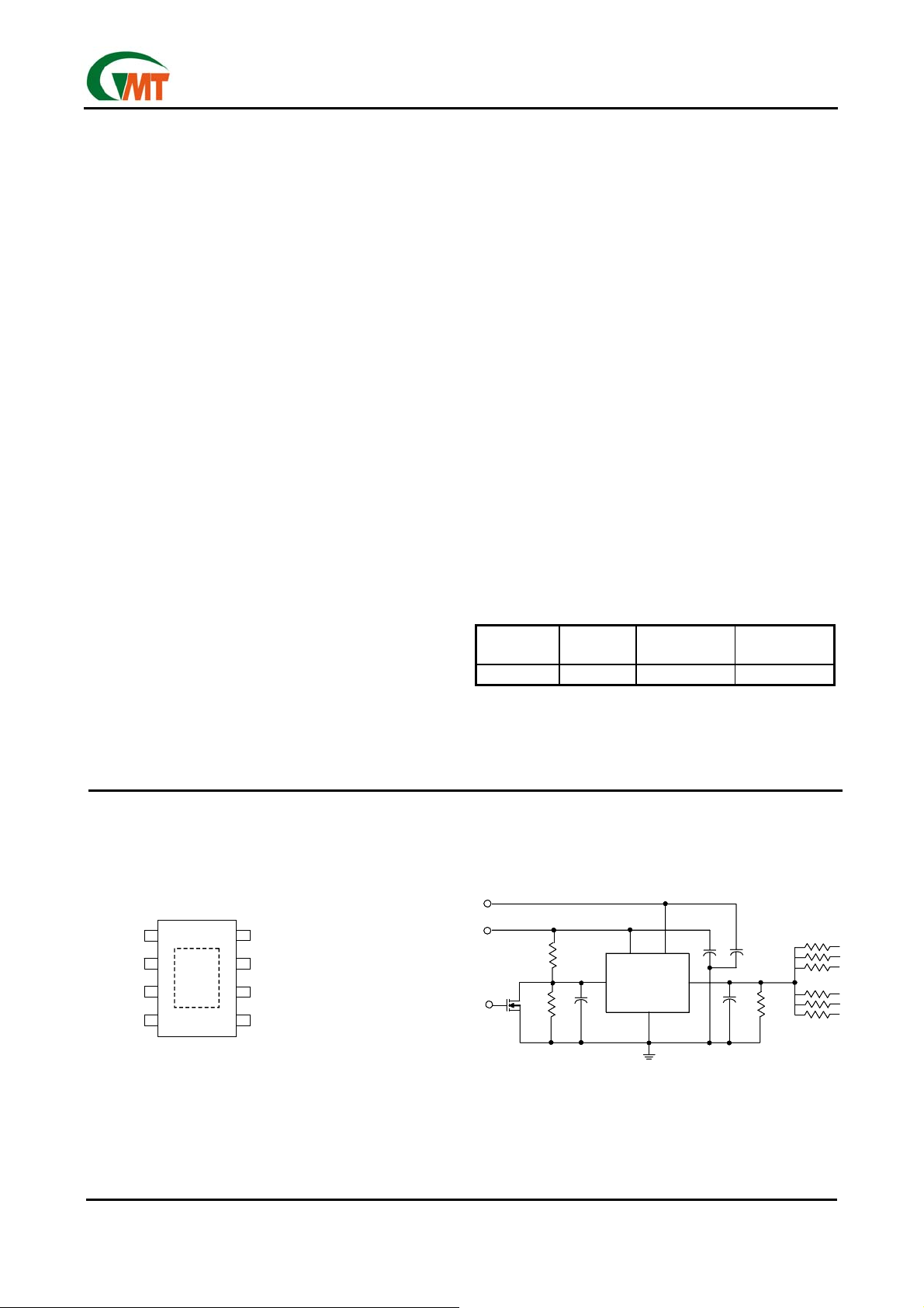
Pin Configuration Typical Application Circuit
=3.3V
=3.3V
V
V
CNTL
CNTL
V
V
=2.5V
=2.5V
IN
IN
1
EN
EN
2N7002
2N7002
R
R
1
1
R
R
2
2
C
C
SS
SS
VIN VCNTL
VIN VCNTL
VREF
VREF
GND
GND
VOUT
VOUT
TEL: 886-3-5788833
http://www.gmt.com.tw
1
1
VIN
VIN
2
2
GND
GND
3
3
VREF
VREF
4
4
VOUT
VOUT
Ver: 1.0
Aug 29, 2006
G2992
G2992
SOP-8(FD)
SOP-8(FD)
8
8
7
7
6
6
5
5
NC
NC
NC
NC
VCNTL
VCNTL
NC
NC
R
R
TT
TT
C
C
C
C
CNTL
CNTL
IN
IN
C
C
R
R
OUT
OUT
DUMMY
DUMMY
Page 2
Global Mixed-mode Technology Inc.
Absolute Maximum Ratings
Supply Voltage
V
to GND. . . . . . . . . . . . . . . . . . . . . . -0.3V to +7V
CNTL
Maximum Junction Temperature, T
Storage Temperature Range, T
STG
Reflow Temperature (soldering, 10sec) . . . . . . 260°C
Thermal Resistance Junction to Ambient, (θ
SOP-8 (FD). . . . . . . . . . . . . . . . . . . . . . . . . . ..50°C/W
Electrostatic Discharge, V
ESD
Human body mode. . . . . . . . . . . . . . . . . . . . . 2000V
Note:
(1)
: Absolute maximum rating indicates limits beyond which damage to the device may occurs.
(2)
: Human body model : C = 100pF, R = 1500Ω, 3 positive pulses plus 3 negative pulses.
(3)
:VIN and V
mustn’t be higher than V
REF
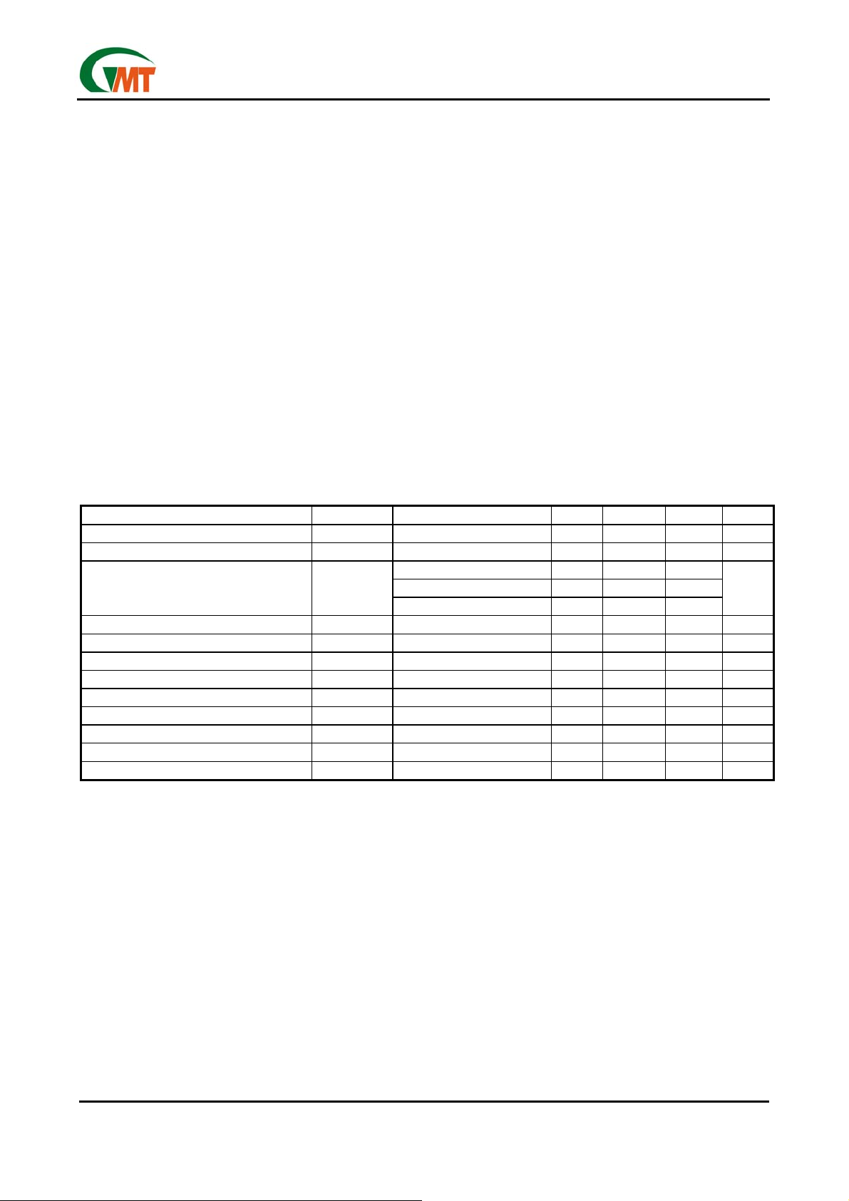
Electrical Characteristics
Specifications with standard typeface are for TA=25°C, VIN=2.5V, V
Unless otherwise specified.
PARAMETER SYMBOL CONDITIONS MIN TYP MAX UNIT
Output Offset Voltage
VTT output voltage
VTT Output Voltage Load Regulation
(DDR I/DDR II)
Input Voltage Range (DDR I/DDR II)
Control Voltage Range (DDR I/DDR II)
Quiescent Current
Quiescent Current in Shutdown
Current Limit
Thermal Shutdown Temperature
Thermal Shutdown Hysteresis
Shutdown High Trigger Level Output
Shutdown Low Trigger Level Output
(1)
. . . . . . . . 150°C
J
. . -65°C to+150°C
)
JA
(2)
.
CNTL
V
-20 0 20 mV
(DDR I/DDR II) --- 1.25/0.9 --- V
I
VTT
|I
VTT
|I
VTT
1.8 2.5/1.8 3.6 V
--- 3.3 5.5 V
I
OUT
V
REF
3 --- --- A
3.3V≦V
--- 20 --- °C
Output active 0.8 --- --- V
Output disable --- --- 0.2 V
V
∆V
V
I
CNTL
I
LIMIT
T
T
OS
TT
TT
V
IN
CNTL
I
SD
TS
HYS
V
IH
V
IL
Recommend Operation Range
Operating Ambient Temperature Range
T
. . . . . . . . . . . . . . . . . . . . . . . . . . . . . -40°C to +85°C
A
V
to GND. . . . . . . . . . . . . . . . . . . . . . 3.3V to 5.5V
CNTL
to GND. . . . . . . . . . . . . . . . . . . . . . . . 1.8V to 3.6V
V
IN
to GND . . . . . . . . . . . . . . . . . . . . . . . .0 to V
V
REF
CNTL
=0, V
|<1.5A,V
|<3A, V
=0A --- 750 1500 µA
<0.2V --- 50 90 µA
=½VIN
REF
=½VIN
REF
=½VIN
REF
≦5.5V --- 160 --- °C
CNTL
G2992
(3)
=3.3V, V
-20 --- 20
-30 --- 30
-40 --- 40
=1.25V, C
REF
OUT
CNTL
=20µF.
mV
Ver: 1.0
Aug 29, 2006
2
TEL: 886-3-5788833
http://www.gmt.com.tw
Page 3
Global Mixed-mode Technology Inc.
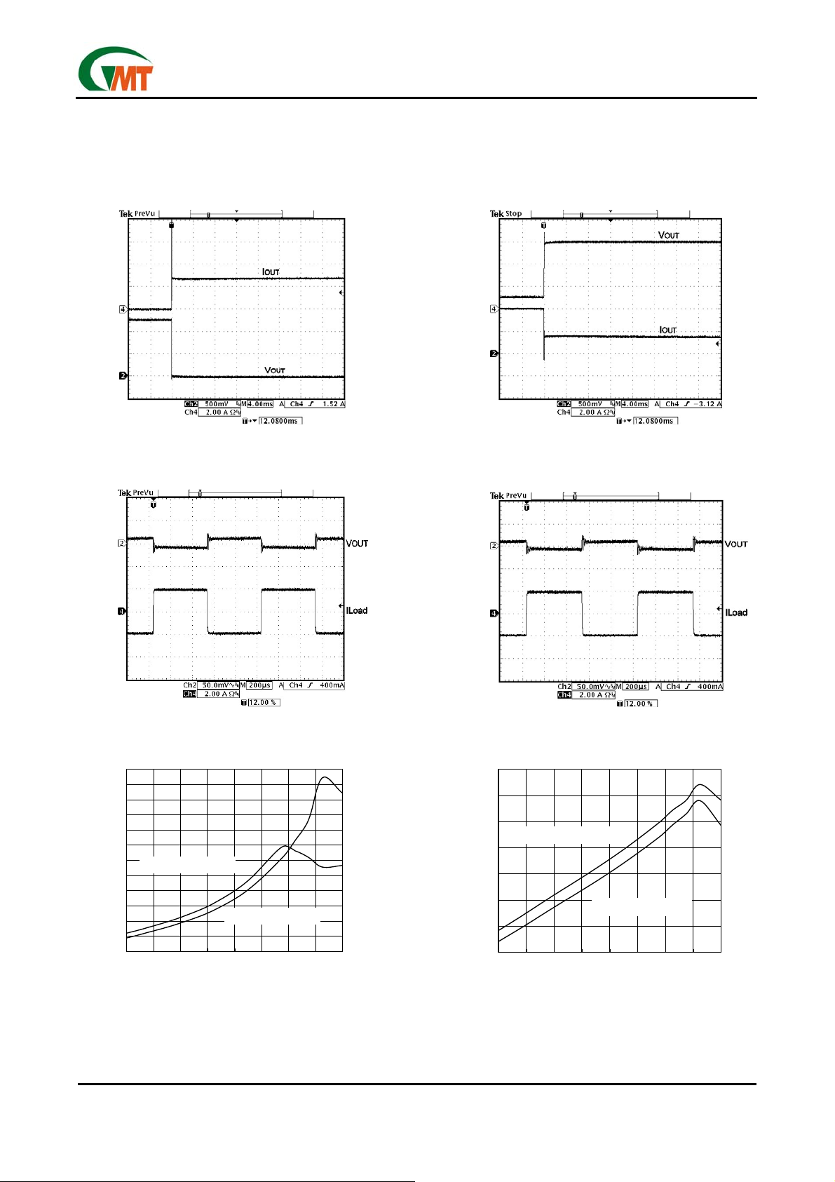
Typical Performance Characteristics
C
=1µF/MLCC/X5R, CIN=22µF/MLCC/X7R, CSS=1µF/MLCC/X5R, C
CNTL
wise noted.
V
is Shorted to GND
OUT
V
=5.0V,VIN=2.5V
CNTL
G2992
=20µF/X5R/MLCC unless other-
OUT
V
is Shorted to VIN (2.5V)
OUT
V
=5.0V,VIN=2.5V
CNTL
V
Load Transient Response
OUT
V
=5.0V,VIN=2.5V
CNTL
V
Load Transient Response
OUT
V
=5.0V,VIN=1.8V
CNTL
Sourcing Current Limit vs Temperature Sourcing Current Limit vs Temperature
5.6
5.4
5.2
5
4.8
4.6
4.4
V
=3.3V,VIN=1.8V
CNTL
4.2
4
3.8
Sourcing Current Limit (A)
3.6
3.4
3.2
-40 -20 0 20 40 60 80 100 120
V
=5.5V,VIN=1.8V
CNTL
Temperature (°C)
4
3.9
3.8
V
=3.3V,VIN=2.5V
3.7
3.6
3.5
Sourcing Current Limit (A)
3.4
3.3
CNTL
V
=5.5V,VIN=2.5V
CNTL
-40 -20 0 20 40 60 80 100 120
Temperature (°C)
Ver: 1.0
Aug 29, 2006
3
TEL: 886-3-5788833
http://www.gmt.com.tw
Page 4
Global Mixed-mode Technology Inc.
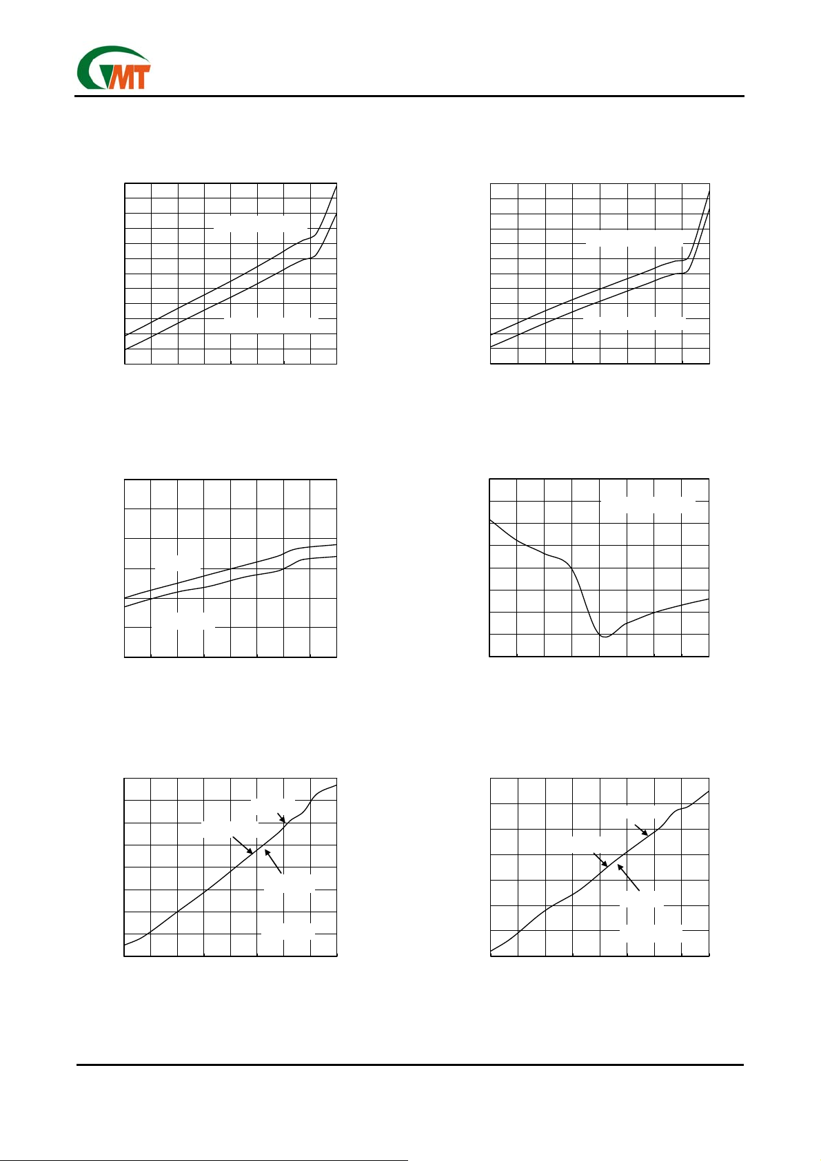
Typical Performance Characteristics (continued)
G2992
Sinking Current Limit vs Temperature
4.4
4.3
4.2
4.1
4
3.9
3.8
3.7
3.6
3.5
Sinking Current Limit (A)
3.4
3.3
3.2
-40 -20 0 20 40 60 80 100 120
V
Shutdown Threshold vs Temperature
REF
0.8
0.7
0.6
V
0.5
0.4
Shutdown Threshold (V)
REF
V
0.3
0.2
-40 -20 0 20 40 60 80 100 120
CNTL
V
CNTL
V
CNTL
V
CNTL
Temperature (°C)
=5V
=3.3V
Temperature (°C)
=5.5V,VIN=1.8V
=3.3V,VIN=1.8V
Sinking Current Limit vs Temperature
4.4
4.3
4.2
4.1
4
3.9
3.8
3.7
3.6
3.5
Sinking Current Limit (A)
3.4
3.3
3.2
-40 -20 0 20 40 60 80 100 120
Supply Current vs Vout Load Current
V
CNTL
1.2
1.15
1.1
1.05
1
0.95
Supply Current (mA)
CNTL
0.9
V
0.85
0.8
-2 -1.5 -1 -0.5 0 0.5 1 1.5 2
V
=5.5V,VIN=2.5V
CNTL
V
=3.3V,VIN=2.5V
CNTL
Temperature (°C)
V
CNTL
Load Current (A)
V
OUT
=5.0V,VIN=1.8V
vs Temperature
R
DS(ON)
0.18
0.17
0.16
0.15
(Ω)
0.14
DS(ON)
R
0.13
0.12
0.11
0.1
-40 -20 0 20 40 60 80 100 120
VIN=0.85V
Temperature (°C)
VIN=0.9V
Ver: 1.0
Aug 29, 2006
VIN=0.8V
V
=3.3V
CNTL
4
R
vs Temperature
DS(ON)
0.16
0.15
0.14
0.13
(Ω)
0.12
DS(ON)
R
0.11
0.1
0.09
-40 -20 0 20 40 60 80 100 120
VIN=0.9V
VIN=0.85V
VIN=0.8V
V
CNTL
Temperature (°C)
=5.0V
TEL: 886-3-5788833
http://www.gmt.com.tw
Page 5
Global Mixed-mode Technology Inc.
Typical Performance Characteristics (continued)
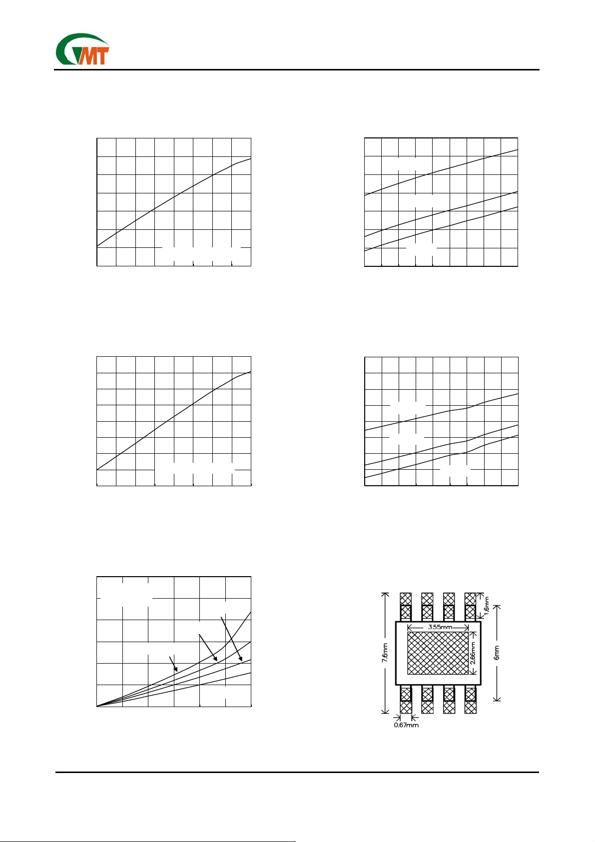
V
Supply Current vs Temperature
CNTL
1
G2992
V
Supply Current vs. V
CNTL
Supply Voltage
1
CNTL
0.95
0.9
0.85
0.8
0.75
Supply Current (mA)
CNTL
V
0.7
0.65
-40-200 20406080100120
Shutdown Current vs Temperature
V
CNTL
62
60
A)
µ
58
56
54
52
Shutdown Current (
50
CNTL
V
48
46
-40-200 20406080100120
V
=5.0V,VIN=2.5V
CNTL
Temperature (°C)
V
=5.0V,VIN=2.5V
CNTL
Temperature (°C)
Supply Current (mA)
CNTL
V
0.95
0.9
0.85
0.8
0.75
0.7
0.65
TA=120°C
TA=25°C
TA=0°C
3.3 3.6 3.9 4.2 4.5 4.8 5.1 5.4 5.7 6
V
Supply Voltage (V)
CNTL
V
Shutdown Current vs V
CNTL
Supply Voltage
69
66
A)
µ
63
60
57
54
Shutdown Current (
51
CNTL
V
48
45
3.3 3.6 3.9 4.2 4.5 4.8 5.1 5.4 5.7 6
TA=120°C
TA=25°C
V
CNTL
TA=0°C
Supply Voltage (V)
CNTL
VIN Dropout Voltage vs Output Current
1.2
V
V
1
0.8
0.6
0.4
Dropout Voltage (V)
0.2
0
00.511.522.53
Ver: 1.0
Aug 29, 2006
REF
CNTL
=0.9V
=3.3V
TA=75°C
TA=125°C
Output Current (A)
TA=25°C
TA=-50°C
5
Recommended Minimum Footprint
SOP-8 (FD)
TEL: 886-3-5788833
http://www.gmt.com.tw
Page 6
Global Mixed-mode Technology Inc.
Pin Description
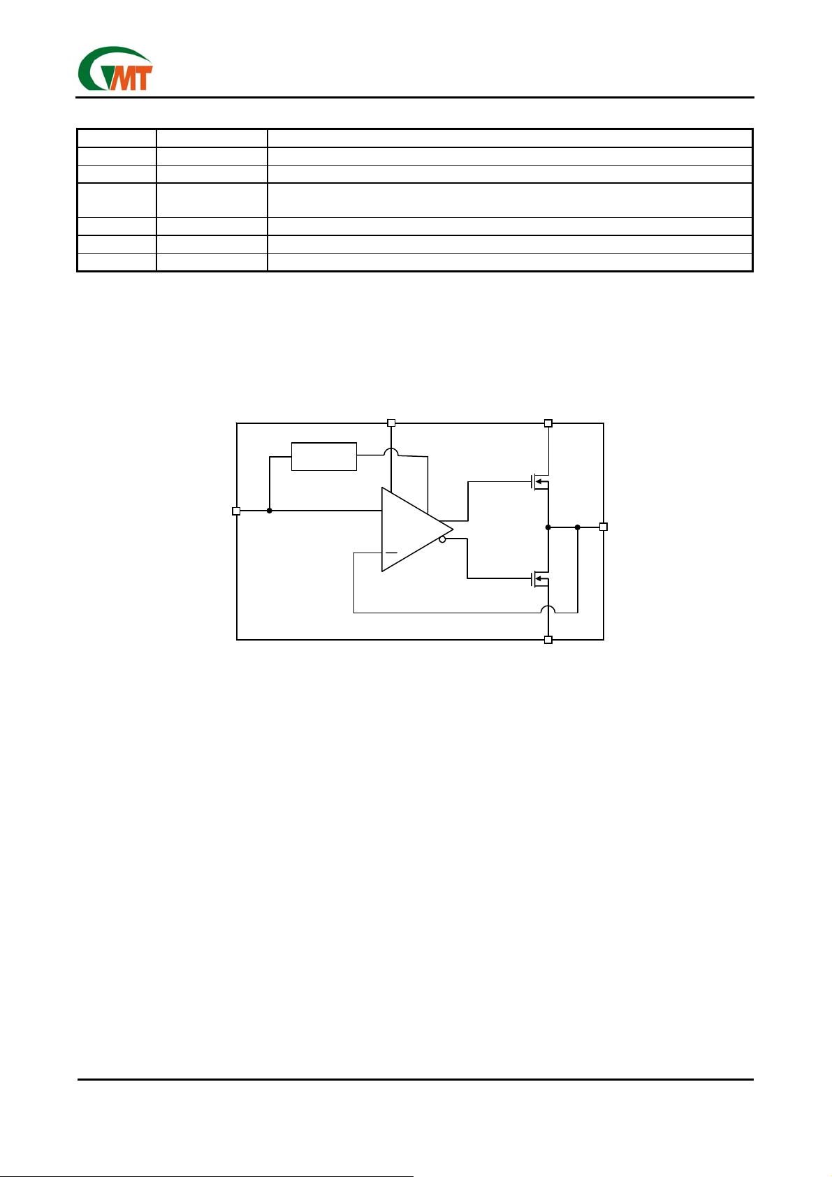
PIN NAME FUNCTION
1 VIN Terminator Power pin.
2 GND Ground
3 VREF
4 VOUT Terminator output pin (VTT voltage supplied)
5,7,8 NC No Connection
6 VCNTL Internal circuit power pin, at least 3.3V
Block Diagram
VREF
VREF
Application Information
Output Capacitor
For stable operation, total capacitance of the V
put terminal can be equal or greater than 20µF. The
output capacitor should be located near V
terminal as close as possible to minimize the effect of
ESR and ESL.
Power on sequence
For safely operation, The G2992 must keep V
voltage larger than VIN, this condition is due to the internal parasitic diodes between V
G2992 will consume large current when V
larger than V
Consideration of the V
The V
REF
.
CNTL
REF
voltage is applied by a buffered mid-rail
Terminator reference input voltage, 1.25V for DDR I, 0.9V for DDR II. Below 0.2V, the chip
will be shutdown.
VIN
VIN
GND
GND
Shutdown
Shutdown
VCNTL
VCNTL
+
+
voltage which is generated by a resistor divider be-
TT
out-
tween V
and GND. Using a capacitor tapped to the
IN
voltage divider can form a low-pass filter. It can in-
output
TT
crease both the soft-start interval and the noise immunity.
Input Capacitor
Adding a capacitance close to V
V
performance when fast load- transient. In general,
TT
1/2 C
Separating the V
is recommended for the VIN capacitance.
OUT
and V
IN
sient performance.
to V
IN
. The
CNTL
voltage is
IN
CNTL
A ceramic capacitance with a value between 1.0µF
Voltage
and 4.7µF close to the V
stabilize the V
CNTL
voltage.
G2992
VOUT
VOUT
pin can improve the
IN
pins will get better tran-
CNTL
pin is recommended to
CNTL
Ver: 1.0
Aug 29, 2006
6
TEL: 886-3-5788833
http://www.gmt.com.tw
Page 7
Global Mixed-mode Technology Inc.
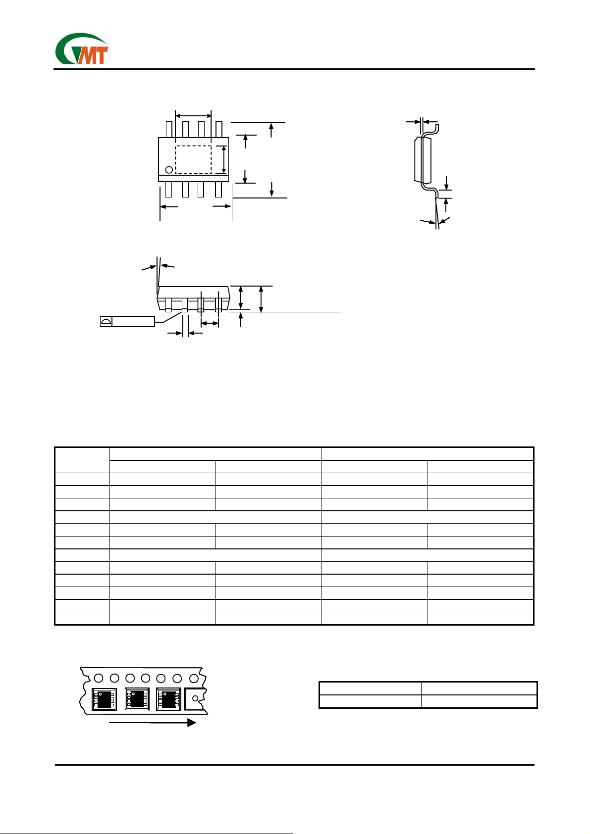
Package Information
0.004MAX.
0.004MAX.0.004MAX.
0.015x45º
0.015x45º
G2992
D1
D1
0.008TYP
0.008TYP
E1
E1
E
E
H
H
L
L
D
D
θ
θ
A2
A2
A
A
SEATING PLANE
SEATING PLANE
A1
e
e
B
B
A1
SOP- 8 (F1) Package
Note:
1. JEDEC Outline: MS-012 AA/E.P. Version: N/A
2. Dimension “D” does not include mold flash, protrusions or gate burrs. Mold flash, protrusions and gate burrs
shall not exceed .15mm (.006in) per side.
3. Dimensions “E” does not include inter-lead flash, or protrusions inter-lead flash and protrusions shall not ex-
ceed .25mm (.010in) per side.
SYMBOL
A 1.35 1.75 0.053 0.069
A1 0.00 0.13 0.000 0.005
A2 ----- 1.50 ----- 0.059
B 0.41TYP 0.016TYP
D 4.80 4.98 0.189 0.196
E 3.81 3.99 0.150 0.157
e 1.27TYP 0.05TYP
H 5.80 6.20 0.228 0.244
L 0.41 1.27 0.016 0.050
θ
D1 ----- 2.29 ----- 0.090
E1 ----- 2.29 ----- 0.090
DIMENSION IN MM DIMENSION IN INCH
MIN. MAX. MIN. MAX.
0º 8º 0º 8º
Taping Specification
PACKAGE Q’TY/REEL
SOP-8 (FD) 2,500 ea
Typical SOP Package Orientation
Typical SOP Package Orientation
GMT Inc. does not assume any responsibility for use of any circuitry described, no circuit patent licenses are implied and GMT Inc. reserves the right at any time without notice to change said circuitry and specifications.
Ver: 1.0
Aug 29, 2006
Feed Direction
Feed Direction
7
TEL: 886-3-5788833
http://www.gmt.com.tw
 Loading...